Äîêóìåíòàöèÿ è îïèñàíèÿ www.docs.chipfind.ru
1
Selection Guide
7C371-143
7C371-110
7C371-83
7C371L-83
7C371-66
7C371L-66
Maximum Propagation Delay, t
PD
(ns)
8.5
10
12
12
15
15
Minimum Set Up, t
S
(ns)
5
6
10
10
12
12
Maximum Clock to Output, t
CO
(ns)
6
6.5
10
10
12
12
Maximum Supply
Current I
CC
(mA)
Commercial
220
175
175
90
175
90
Current, I
CC
(mA)
Military/Ind.
220
110
220
110
Shaded area contains preliminary information.
Cypress Semiconductor Corporation
D
3901 North First Street
D
S an Jose
D
CA 95134
D
408-943-2600
December 1993 - Revised August 1995
CY7C371
UltraLogict 32 Macrocell Flash CPLD
7c371: Tuesday, May 26, 1992
Revision: August 9, 1995
Features
D
32 macrocells in two logic blocks
D
32 I/O pins
D
6 dedicated inputs including 2 clock
pins
D
No hidden delays
D
High speed
f
MAX
= 143 MHz
t
PD
= 8.5 ns
t
S
= 5 ns
t
CO
= 6 ns
D
Electrically alterable FLASH
technology
D
Available in 44 pin PLCC, CLCC, and
TQFP packages
D
Pin compatible with the CY7C372
Functional Description
The CY7C371 is a Flash erasable Complex
Programmable Logic Device (CPLD) and
is part of the F
LASH
370 family of high den
sity, high speed CPLDs. Like all members
of the F
LASH
370 family, the CY7C371 is
designed to bring the ease of use and high
performance of the 22V10 to high density
CPLDs.
The 32 macrocells in the CY7C371 are di
vided between two logic blocks. Each logic
block includes 16 macrocells, a 72 x 86
product term array, and an intelligent
product term allocator.
The logic blocks in the F
LASH
370 architec
ture are connected with an extremely fast
and predictable routing resource the
Programmable
Interconnect
Matrix
(PIM). The PIM brings flexibility, rout
ability, speed, and a uniform delay to the
interconnect.
Like all members of the F
LASH
370 family,
the CY7C371 is rich in I/O resources.
Each macrocell in the device features an
associated I/O pin, resulting in 32 I/O pins
on the CY7C371. In addition, there are
four dedicated inputs and two input/clock
pins.
Finally, the CY7C371 features a very sim
ple timing model. Unlike other high den
sity CPLD architectures, there are no hid
den speed delays such as fanout effects, in
terconnect delays, or expander delays. Re
gardless of the number of resources used
or the type of application, the timing pa
rameters on the CY7C371 remain the
same.
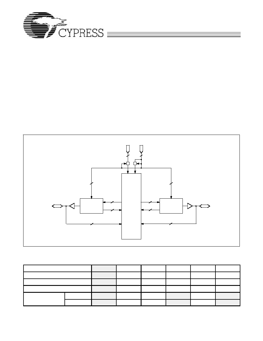
Logic Block Diagram
7c371 1
PIM
4
INPUT
MACROCELLS
2
CLOCK
INPUTS
INPUTS
LOGIC
BLOCK
A
LOGIC
BLOCK
B
2
2
36
16
16
36
16 I/Os
16 I/Os
16
16
INPUT/CLOCK
MACROCELLS
I/O
0
-I/O
15
I/O
16
-I/O
31
CY7C371
7c371: Tuesday, May 26, 1992
Revision: August 9, 1995
2
7c371 2
I/O
27
I/O
26
I/O
25
I/O
24
CLK1/I
5
GND
I
4
I
3
I/O
23
I/O
22
I/O
21
I/O
5
I/O
6
I/O
7
I
0
I
1
GND
CLK0/I
2
I/O
8
I/O
9
I/O
10
I/O
11
GND
I/O
20
I/O
2
GND
V CC
V
CC
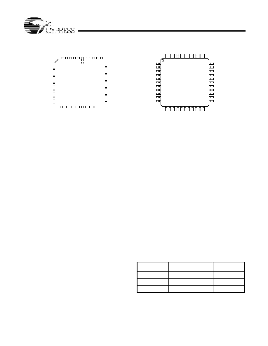
Pin Configurations
I/O
3
I/O
4
I/O
1
I/O
0
I/O
29
I/O
30
I/O
31
I/O
28
I/O
19
I/O
18
I/O
17
I/O
16
I/O
15
I/O
14
I/O
13
I/O
12
6 5
3
4
2
8
9
7
10
11
1 44
18
15
16
14
13
12
17
19 20
22
21
23 24
27
26
28
25
31
30
29
32
33
34
39
37
38
36
35
43 42
40
41
I/O
2
GND
V CC
I/O
3
I/O
4
I/O
1
I/O
0
I/O
29
I/O
30
I/O
31
I/O
28
I/O
27
I/O
26
I/O
25
I/O
24
CLK1/I
5
GND
I
4
I
3
I/O
23
I/O
22
I/O
21
GND
I/O
20
V
CC
I/O
19
I/O
18
I/O
17
I/O
16
I/O
15
I/O
14
I/O
13
I/O
12
I/O
5
I/O
6
I/O
7
I
0
I
1
GND
CLK0/I
2
I/O
8
I/O
9
I/O
10
I/O
11
8
9
7
10
11
3
4
2
5
6
1
18 19 20
22
21
13 14 15
17
16
12
31
30
29
32
33
26
25
24
27
28
23
44 43 42
40
41
39 38 37
35
36
34
7c371 3
PLCC/CLCC
Top View
TQFP
Top View
Logic Block
The number of logic blocks distinguishes the members of the
F
LASH
370 family. The CY7C371 includes two logic blocks. Each
logic block is constructed of a product term array, a product term
allocator, and 16 macrocells.
Product Term Array
The product term array in the F
LASH
370 logic block includes 36 in
puts from the PIM and outputs 86 product terms to the product
term allocator. The 36 inputs from the PIM are available in both
positive and negative polarity, making the overall array size 72 x 86.
This large array in each logic block allows for very complex func
tions to be implemented in a single pass through the device.
Product Term Allocator
The product term allocator is a dynamic, configurable resource
that shifts product terms to macrocells that require them. Any
number of product terms between 0 and 16 inclusive can be as
signed to any of the logic block macrocells (this is called product
term steering). Furthermore, product terms can be shared among
multiple macrocells. This means that product terms that are com
mon to more than one output can be implemented in a single prod
uct term. Product term steering and product term sharing help to
increase the effective density of the F
LASH
370 CPLDs. Note that
product term allocation is handled by software and is invisible to
the user.
I/O Macrocell
Each of the macrocells on the CY7C371 has a separate associated
I/O pin. The input to the macrocell is the sum of between 0 and 16
product terms from the product term allocator. The macrocell in
cludes a register that can be optionally bypassed. It also has polar
ity control, and two global clocks to trigger the register. The ma
crocell also features a separate feedback path to the PIM so that
the register can be buried if the I/O pin is used as an input.
Programmable Interconnect Matrix
The Programmable Interconnect Matrix (PIM) connects the two
logic blocks on the CY7C371 to the inputs and to each other. All
inputs (including feedbacks) travel through the PIM. There is no
speed penalty incurred by signals traversing the PIM.
Design Tools
Development software for the CY7C371 is available from Cy
press's Warp2, Warp2+, and Warp3 software packages. All of these
products are based on the IEEE standard VHDL language. Cy
press also actively supports third party design tools such as
ABELt, CUPLt, MINC, and LOG/iCt. Please contact your lo
cal Cypress representative for further information.
Maximum Ratings
(Above which the useful life may be impaired. For user guidelines,
not tested.)
Storage Temperature
-65_C to +150_C
. . . . . . . . . . . . . . . . . . .
Ambient Temperature with
Power Applied
-55_C to +125_C
. . . . . . . . . . . . . . . . . . . . . . . .
Supply Voltage to Ground Potential
-0.5V to +7.0V
. . . . . . . . .
DC Voltage Applied to Outputs
in High Z State
-0.5V to +7.0V
. . . . . . . . . . . . . . . . . . . . . . . . . .
DC Input Voltage
-0.5V to +7.0V
. . . . . . . . . . . . . . . . . . . . . . . .
DC Program Voltage
12.5V
. . . . . . . . . . . . . . . . . . . . . . . . . . . . . .
Output Current into Outputs (LOW)
16 mA
. . . . . . . . . . . . . . .
Static Discharge Voltage
>2001V
. . . . . . . . . . . . . . . . . . . . . . . .
(per MIL STD 883, Method 3015)
Latch Up Current
>200 mA
. . . . . . . . . . . . . . . . . . . . . . . . . . . .
Operating Range
Range
Ambient
Temperature
V
CC
Commercial
0_C to +70_C
5V ± 5%
Military
[1]
-55_C to +125_C
5V ± 10%
Industrial
-40_C to +85_C
5V ± 10%
Note:
1. T
A
is the instant on" case temperature.
CY7C371
7c371: Tuesday, May 26, 1992
Revision: August 9, 1995
3
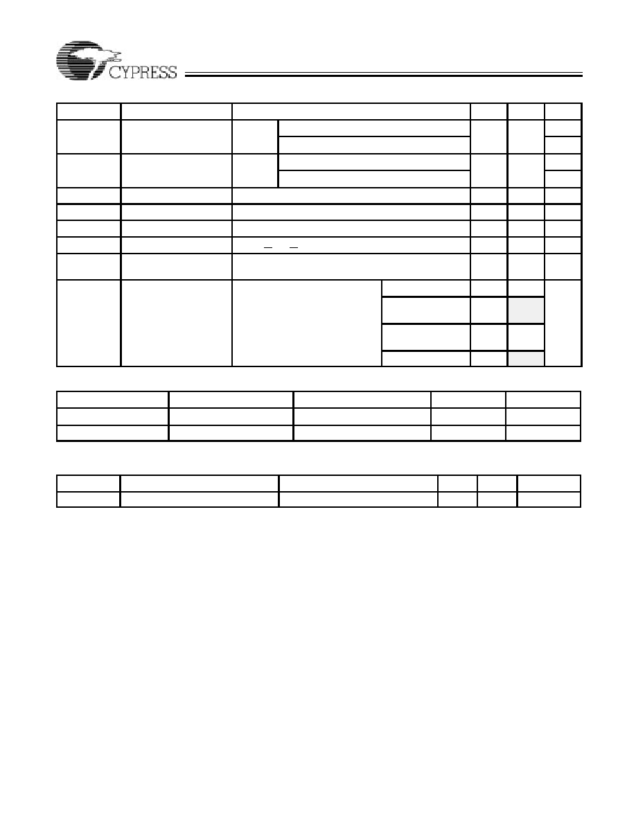
Electrical Characteristics
Over the Operating Range
[2]
Parameter
Description
Test Conditions
Min.
Max.
Unit
V
OH
Output HIGH Voltage
V
CC
=
Min
I
OH
= -3.2 mA (Com'l/Ind)
2.4
V
Min.
I
OH
= -2.0 mA (Mil)
V
V
OL
Output LOW Voltage
V
CC
=
Min
I
OL
= 16 mA (Com'l/Ind)
0.5
V
Min.
I
OL
= 12 mA (Mil)
V
V
IH
Input HIGH Voltage
Guaranteed Input Logical HIGH Voltage for all inputs
[3]
2.0
7.0
V
V
IL
Input LOW Voltage
Guaranteed Input Logical LOW Voltage for all inputs
[2]
-0.5
0.8
V
I
IX
Input Load Current
GND V
I
V
CC
-10
+10
mA
I
OZ
Output Leakage Current
GND < V
O
< V
CC
, Output Disabled
-50
+50
mA
I
OS
Output Short
Circuit Current
[4, 5]
V
CC
= Max., V
OUT
= 0.5V
-30
-90
mA
I
CC
Power Supply Current
V
CC
= Max., I
OUT
= 0 mA,
f = 1 mHz V
IN
= GND V
CC[6]
Com'l
175
mA
f = 1 mHz, V
IN
= GND, V
CC[6]
Com'l L"
-66, -83
90
Com'l-143,
Mil/Ind
220
Ind L" -66, -83
110
Capacitance
[4]
Parameter
Description
Test Conditions
Max.
Unit
C
IN
Input Capacitance
V
IN
= 5.0V at f=1 MHz
10
pF
C
OUT
Output Capacitance
V
OUT
= 5.0V at f = 1 MHz
12
pF
Endurance Characteristics
[4]
Parameter
Description
Test Conditions
Min.
Max.
Unit
N
Minimum Reprogramming Cycles
Normal Programming Conditions
100
Cycles
Notes:
1. See the last page of this specification for Group A subgroup testing in
formation.
2. These are absolute values with respect to device ground. All over
shoots due to system or tester noise are included.
3. Not more than one output should be tested at a time. Duration of the
short circuit should not exceed 1 second. V
OUT
= 0.5V has been cho
sen to avoid test problems caused by tester ground degradation.
4. Tested initially and after any design or process changes that may affect
these parameters.
5. Measured with 16 bit counter programmed into each logic block.
CY7C371
7c371: Tuesday, May 26, 1992
Revision: August 9, 1995
4
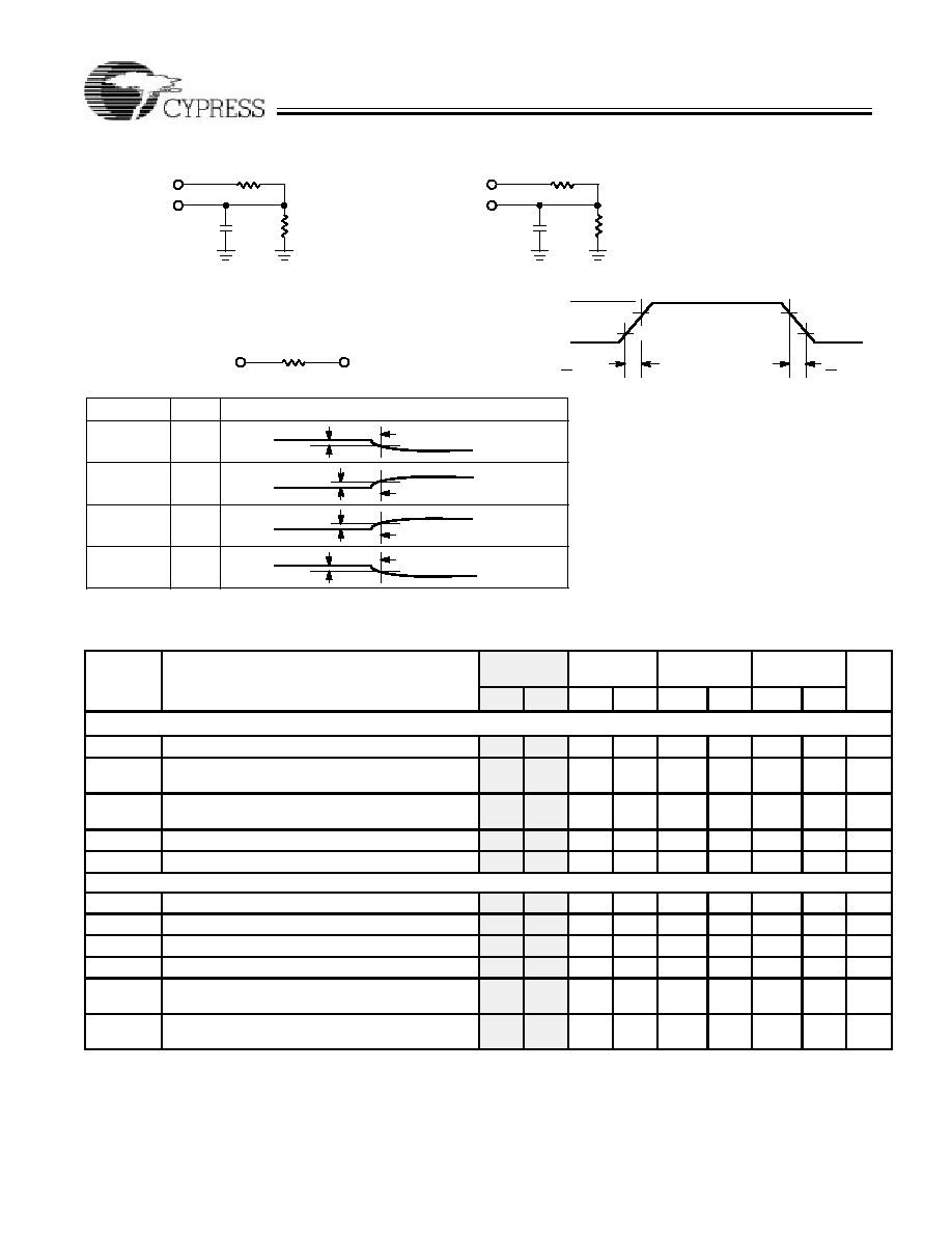
AC Test Loads and Waveforms
7c371 4
7c371 5
90%
10%
3.0V
GND
90%
10%
ALL INPUT PULSES
5V
OUTPUT
35 pF
INCLUDING
JIG AND
SCOPE
5V
OUTPUT
5 pF
INCLUDING
JIG AND
SCOPE
(a)
(b)
< 2 ns
< 2 ns
OUTPUT
238W (COM'L)
319W (MIL)
170W (COM'L)
236W (MIL)
99W (COM'L)
136W (MIL)
Equivalent to:
THÉVENIN EQUIVALENT
2.08V (COM'L)
2.13V (MIL)
238W (COM'L)
319W (MIL)
170W (COM'L)
236W (MIL)
(c)
7c371 6
Parameter
V
X
Output Waveform Measurement Level
t
ER (-)
1.5V
V
OH
0.5V
V
X
0.5V
t
ER (+)
2.6V
V
OL
V
X
t
EA (+)
1.5V
0.5V
t
EA (-)
V
thc
V
X
V
OL
0.5V
V
X
V
OH
7c371 7
7c371 8
7c371 9
7c371 10
(d) Test Waveforms
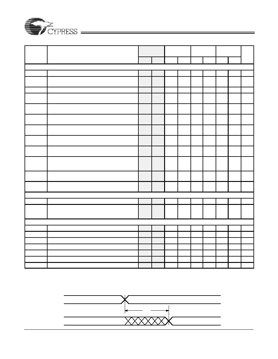
Switching Characteristics
Over the Operating Range
[7]
7C371-143
7C371-110
7C371-83
7C371L-83
7C371-66
7C371L-66
Parameter
Description
Min. Max. Min. Max. Min. Max. Min. Max. Unit
Combinatorial Mode Parameters
t
PD
Input to Combinatorial Output
8.5
10
12
15
ns
t
PDL
Input to Output Through Transparent Input or
Output Latch
11.5
13
18
22
ns
t
PDLL
Input to Output Through Transparent Input and
Output Latches
13.5
15
20
24
ns
t
EA
Input to Output Enable
13
14
19
24
ns
t
ER
Input to Output Disable
13
14
19
24
ns
Input Registered/Latched Mode Parameters
t
WL
Clock or Latch Enable Input LOW Time
[4]
2.5
3
4
5
ns
t
WH
Clock or Latch Enable Input HIGH Time
[4]
2.5
3
4
5
ns
t
IS
Input Register or Latch Set Up Time
2
2
3
4
ns
t
IH
Input Register or Latch Hold Time
2
2
3
4
ns
t
ICO
Input Register Clock or Latch Enable to Combina
torial Output
12
14
19
24
ns
t
ICOL
Input Register Clock or Latch Enable to Output
Through Transparent Output Latch
14
16
21
26
ns
Shaded area contains preliminary information.
Note:
6. All AC parameters are measured with 16 outputs switching.
7. This specification is intended to guarantee interface compatibility of
the other members of the CY7C370 family with the CY7C371. This
specification is met for the devices operating at the same ambient tem
perature and at the same power supply voltage.
CY7C371
7c371: Tuesday, May 26, 1992
Revision: August 9, 1995
5
Switching Characteristics
Over the Operating Range
[6]
(continued)
7C371-143
7C371-110
7C371-83
7C371L-83
7C371-66
7C371L-66
Parameter
Description
Min. Max. Min. Max. Min. Max. Min. Max. Unit
Output Registered/Latched Mode Parameters
t
CO
Clock or Latch Enable to Output
6
6.5
10
12
ns
t
S
Set Up Time from Input to Clock or Latch
Enable
5
6
10
12
ns
t
H
Register or Latch Data Hold Time
0
0
0
0
ns
t
CO2
Output Clock or Latch Enable to Output Delay
(Through Memory Array)
12
14
19
24
ns
t
SCS
Output Clock or Latch Enable to Output Clock or
Latch Enable (Through Memory Array)
7
9
12
15
ns
t
SCS2
Output Clock Through Array to Output Clock
(2 Pass Delay)
[4]
13
16.5
21
27
ns
t
SL
Set Up Time from Input Through Transparent
Latch to Output Register Clock or Latch Enable
9
10
12
15
ns
t
HL
Hold Time for Input Through Transparent Latch
from Output Register Clock or Latch Enable
0
0
0
0
ns
f
MAX1
Maximum Frequency with Internal Feedback
(Least of 1/t
SCS
, 1/(t
S
+ t
H
), or 1/t
CO
)
[4]
143
111
83.3
66.6
MHz
f
MAX2
Maximum Frequency Data Path in Output Regis
tered/Latched Mode (Lesser of 1/(t
WL
+ t
WH
),
1/(t
S
+ t
H
), or 1/t
CO
)
[4]
166.7
153.8
100
83.3
MHz
f
MAX3
Maximum Frequency with external feedback
(Lesser of 1/(t
CO
+ t
S
) and 1/(t
WL
+ t
WH
))
[4]
91
80
50
41.6
MHz
t
OH
-t
IH
37x
Output Data Stable from Output clock Minus
Input Register Hold Time for 7C37x
[4, 8]
0
0
0
0
ns
Pipelined Mode Parameters
t
ICS
Input Register Clock to Output Register Clock
7
9
12
15
ns
f
MAX4
Maximum Frequency in Pipelined Mode (Least of
1/(t
CO
+ t
IS
), 1/t
ICS
, 1/(t
WL
+ t
WH
), 1/(t
IS
+ t
IH
),
or 1/t
SCS
)
125
111
76.9
62.5
MHz
Reset/Preset Parameters
t
RW
Asynchronous Reset Width
[4]
8
10
15
20
ns
t
RR
Asynchronous Reset Recovery Time
[4]
10
12
17
22
ns
t
RO
Asynchronous Reset to Output
14
16
21
26
ns
t
PW
Asynchronous Preset Width
[4]
8
10
15
20
ns
t
PR
Asynchronous Preset Recovery Time
[4]
10
12
17
22
ns
t
PO
Asynchronous Preset to Output
14
16
21
26
ns
t
POR
Power On Reset
[4]
1
1
1
1
ms
Shaded area contains preliminary information.
Switching Waveforms
Combinatorial Output
t
PD
7c371 11
INPUT
COMBINATORIAL
OUTPUT