 | –≠–ª–µ–∫—Ç—Ä–æ–Ω–Ω—ã–π –∫–æ–º–ø–æ–Ω–µ–Ω—Ç: CY7C466A | –°–∫–∞—á–∞—Ç—å:  PDF PDF  ZIP ZIP |
Asynchronous, Cascadable 8K/16K/32K/64K x9 FIFOs
CY7C460A/CY7C462A
CY7C464A/CY7C466A
Cypress Semiconductor Corporation
∑
3901 North First Street
∑
San Jose
∑
CA 95134
∑
408-943-2600
Document #: 38-06011 Rev. *A
Revised December 26, 2002
60A
Features
∑ High-speed, low-power, first-in first-out (FIFO)
memories
∑ 8K x 9 FIFO (CY7C460A)
∑ 16K x 9 FIFO (CY7C462A)
∑ 32K x 9 FIFO (CY7C464A)
∑ 64K x 9 FIFO (CY7C466A)
∑ 10-ns access times, 20-ns read/write cycle times
∑ High-speed 50-MHz read/write independent of
depth/width
∑ Low operating power
-- I
CC
= 60 mA
-- I
SB
=8 mA
∑ Asynchronous read/write
∑ Empty and Full flags
∑ Half Full flag (in standalone mode)
∑ Retransmit (in standalone mode)
∑ TTL-compatible
∑ Width and Depth Expansion Capability
∑ 5V
±
10% supply
∑ PLCC, LCC, 300-mil and 600-mil DIP packaging
∑ Three-state outputs
∑ Pin compatible density upgrade to CY7C42X/46X family
∑ Pin compatible and functionally equivalent to IDT7205,
IDT7206, IDT7207, IDT7208
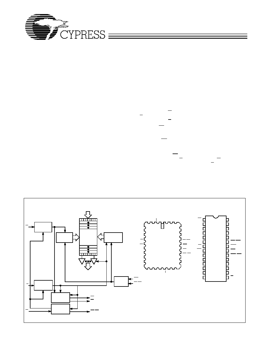
Functional Description
The CY7C460A, CY7C462A, CY7C464A, and CY7C466A are
respectively, 8K, 16K, 32K, and 64K words by 9-bit wide first-in
first-out (FIFO) memories. Each FIFO memory is organized
such that the data is read in the same sequential order that it
was written. Full and Empty flags are provided to prevent over-
run and underrun. Three additional pins are also provided to
facilitate unlimited expansion in width, depth, or both. The
depth expansion technique steers the control signals from one
device to another by passing tokens.
The read and write operations may be asynchronous; each
can occur at a rate of up to 50 MHz. The write operation occurs
when the Write (W) signal is LOW. Read occurs when Read
(R) goes LOW. The nine data outputs go to the high-imped-
ance state when R is HIGH.
A Half Full (HF) output flag is provided that is valid in the stan-
dalone (single device) and width expansion configurations. In
the depth expansion configuration, this pin provides the ex-
pansion out (XO) information that is used to tell the next FIFO
that it will be activated.
In the standalone and width expansion configurations, a LOW
on the Retransmit (RT) input causes the FIFOs to retransmit
the data. Read Enable (R) and Write Enable (W) must both be
HIGH during a retransmit cycle, and then R is used to access
the data.
The CY7C460A, CY7C462A, CY7C464A, and CY7C466A are
fabricated using Cypress's advanced 0.5µ RAM3 CMOS tech-
nology. Input ESD protection is greater than 2000V and
latch-up is prevented by careful layout and the use of guard
rings.
32K x
Logic Block Diagram
Pin Configurations
1
2
3
4
5
6
7
8
9
10
11
12
15
16
17
18
19
20
24
23
22
21
13
14
25
28
27
26
Top View
DIP
W
D
8
D
3
D
2
D
1
D
0
XI
FF
Q
0
Q
1
Q
2
GND
V
CC
D
4
FL/RT
MR
EF
XO/HF
Q
7
R
PLCC/LCC
Top View
Q
3
Q
8
D
5
D
6
D
7
Q
6
Q
5
Q
4
4
3
2
1
32 31 30
14 15 16 17 18 19 20
5
6
7
8
9
10
11
12
13
29
28
27
26
25
24
23
22
21
FL/RT
MR
EF
XO/HF
Q
7
D
6
Q
6
D
7
NC
READ
CONTROL
WRITE
CONTROL
WRITE
POINTER
RESET
LOGIC
EXPANSION
LOGIC
RAM ARRAY
8K x 9
16K x 9
9
DATAINPUTS
(D
0
-
D
8
)
THREE≠
STATE
BUFFERS
DATA OUTPUTS
(Q
0
-Q
8
)
W
READ
POINTER
FLAG
LOGIC
R
XI
EF
FF
XO/HF
MR
FL/RT
D
2
D
1
D
0
XI
FF
Q
0
Q
1
NC
Q
2
D
D
W
NC
V
D
D
3
8
cc
4
5
Q
Q
GND
NC
R
Q
Q
3
8
4
5
C46XA≠1
C46XA≠2
C46XA≠3
7C460A
7C462A
7C464A
7C460A
7C462A
7C464A
64K x 9
7C466A
7C466A
DUAL PORT
CY7C460A/CY7C462A
CY7C464A/CY7C466A
Document #: 38-06011 Rev. *A
Page 2 of 15
Maximum Ratings
[1]
(Above which the useful life may be impaired. For user guide-
lines, not tested.)
Storage Temperature ..................................≠65
∞
C to +150
∞
C
Ambient Temperature with
Power Applied.............................................≠55
∞
C to +125
∞
C
Supply Voltage to Ground Potential ............... ≠0.5V to +7.0V
DC Voltage Applied to Outputs
in High Z State ............................................... ≠0.5V to +7.0V
DC Input Voltage............................................ ≠0.5V to +7.0V
Power Dissipation ..........................................................1.0W
Output Current, into Outputs (LOW)............................ 20 mA
Static Discharge Voltage............................................ >2001V
(per MIL-STD-883, Method 3015)
Latch-Up Current ..................................................... >200 mA
Selection Guide
7C460A-10
7C462A-10
7C464A-10
7C466A-10
7C460A-15
7C462A-15
7C464A-15
7C466A-15
7C460A-25
7C462A-25
7C464A-25
7C466A-25
Frequency (MHz)
50
40
28.5
Maximum Access Time (ns)
10
15
25
Operating Range
Range
Ambient
Temperature
V
CC
Commercial
0
∞
C to + 70
∞
C
5V
±
10%
Industrial
≠40
∞
C to +85
∞
C
5V
±
10%
Military
[2]
≠55
∞
C to +125
∞
C
5V
±
10%
Electrical Characteristics
Over the Operating Range
[3]
Parameter
Description
Test Conditions
7C460A/462A/464A/466A
(-10,-15,-25)
Unit
Min.
Max.
V
OH
Output HIGH Voltage
V
CC
= Min., I
OH
=
-
2.0 mA
2.4
V
V
OL
Output LOW Voltage
V
CC
= Min., I
OL
= 8.0 mA
0.4
V
V
IH
Input HIGH Voltage
2.2
V
CC
V
V
IL
Input LOW Voltage
-
0.5
0.8
V
I
IX
Input Leakage Current
GND < V
I
< V
CC
≠10
+10
µ
A
I
OZ
Output Leakage Current
R > V
IH
, GND < V
O
< V
CC
≠10
+10
µ
A
I
CC
Operating Current
V
CC
= Max.,
I
OUT
= 0 mA, Freq. = 20 MHz
60
mA
I
SB
Standby Current
All Inputs = V
IH
min.
8
mA
Capacitance
[5]
Parameter
Description
Test Conditions
Max.
Unit
C
IN
Input Capacitance
T
A
= 25
∞
C, f = 1 MHz,
V
CC
= 4.5V
10
pF
C
OUT
Output Capacitance
12
pF
Notes:
1.
The Voltage on any input or I/O pin cannot exceed the power pin during power-up.
2.
T
A
is the "instant on" case temperature.
3.
See the last page of this specification for Group A subgroup testing information.
4.
For test purposes, not more than one output at a time should be shorted. Short circuit test duration should not exceed 1 second.
5.
Tested initially and after any design or process changes that may affect these parameters.
CY7C460A/CY7C462A
CY7C464A/CY7C466A
Document #: 38-06011 Rev. *A
Page 3 of 15
AC Test Loads and Waveforms
3.0V
5V
OUTPUT
R1 500
R2
333
30 pF
INCLUDING
JIG AND
SCOPE
GND
90%
10%
90%
10%
5 ns
5 ns
5V
OUTPUT
R1 500
R2
333
5 pF
INCLUDING
JIG AND
SCOPE
OUTPUT
2V
Equivalent to:
TH… VENIN EQUIVALENT
(b)
C460A≠4
C460A≠5
C460A≠6
(a)
ALL INPUT PULSES
200
Switching Characteristics
Over the Operating Range
[3, 6]
Parameter
Description
7C460A-10
7C462A-10
7C464A-10
7C466A-10
7C460A-15
7C462A-15
7C464A-15
7C466A-15
7C460A-25
7C462A-25
7C464A-25
7C466A-25
Unit
Min.
Max.
Min.
Max.
Min.
Max.
t
RC
Read Cycle Time
20
25
35
ns
t
A
Access Time
10
15
25
ns
t
RR
Read Recovery Time
10
10
10
ns
t
PR
Read Pulse Width
10
15
25
ns
t
LZR
Read LOW to Low Z
3
3
3
ns
t
DVR
[7]
Data Valid After Read HIGH
3
3
3
ns
t
HZR
[7]
Read HIGH to High Z
15
15
18
ns
t
WC
Write Cycle Time
20
25
35
ns
t
PW
Write Pulse Width
10
15
25
ns
t
HWZ
Write HIGH to Low Z
5
5
5
ns
t
WR
Write Recovery Time
10
10
10
ns
t
SD
Data Set-Up Time
9
9
9
ns
t
HD
Data Hold Time
0
0
0
ns
t
MRSC
MR Cycle Time
20
25
35
ns
t
PMR
MR Pulse Width
10
15
25
ns
t
RMR
MR Recovery Time
10
10
10
ns
t
RPW
Read HIGH to MR HIGH
10
15
25
ns
t
WPW
Write HIGH to MR HIGH
10
15
25
ns
t
RTC
Retransmit Cycle Time
20
25
35
ns
t
PRT
Retransmit Pulse Width
10
15
25
ns
t
RTR
Retransmit Recovery Time
10
10
10
ns
t
EFL
MR to EF LOW
20
25
35
ns
t
HFH
MR to HF HIGH
20
25
35
ns
t
FFH
MR to FF HIGH
20
25
35
ns
t
REF
Read LOW to EF LOW
10
15
25
ns
t
RFF
Read HIGH to FF HIGH
10
15
25
ns
Notes:
6.
Test conditions assume signal transmission time of 5 ns or less, timing reference levels of 1.5V and output loading of the specified I
OL
/I
OH
and 30-pF load
capacitance, as in part (a) of AC Test Loads, unless otherwise specified.
7.
t
HZR
and t
DVR
use capacitance loading as in part (b) of AC Test Loads.
CY7C460A/CY7C462A
CY7C464A/CY7C466A
Document #: 38-06011 Rev. *A
Page 4 of 15
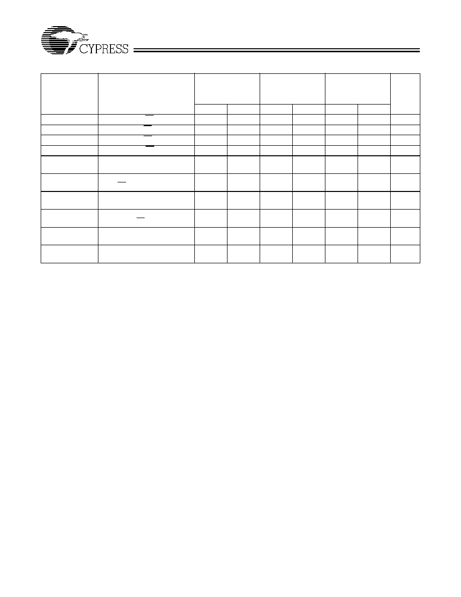
t
WEF
Write HIGH to EF HIGH
10
15
25
ns
t
WFF
Write LOW to FF LOW
10
15
25
ns
t
WHF
Write LOW to HF LOW
10
15
35
ns
t
RHF
Read HIGH to HF HIGH
10
15
35
ns
t
RAE
Effective Read from Write
HIGH
10
15
25
ns
t
RPE
Effective Read Pulse Width
After EF HIGH
10
15
25
ns
t
WAF
Effective Write from Read
HIGH
10
15
25
ns
t
WPF
Effective Write Pulse
Width After FF HIGH
10
15
25
ns
t
XOL
Expansion Out LOW
Delay from Clock
10
15
25
ns
t
XOH
Expansion Out HIGH
Delay from Clock
10
15
25
ns
Switching Characteristics
Over the Operating Range
[3, 6]
(continued)
Parameter
Description
7C460A-10
7C462A-10
7C464A-10
7C466A-10
7C460A-15
7C462A-15
7C464A-15
7C466A-15
7C460A-25
7C462A-25
7C464A-25
7C466A-25
Unit
Min.
Max.
Min.
Max.
Min.
Max.
CY7C460A/CY7C462A
CY7C464A/CY7C466A
Document #: 38-06011 Rev. *A
Page 5 of 15
Switching Waveforms
[7]
Notes:
8.
A HIGH-to-LOW transition of either the write or read strobe causes a HIGH-to-LOW transition of the responding flag. Correspondingly, a LOW-to-HIGH strobe
transition causes a LOW-to-HIGH flag transition.
9.
W and R = V
IH
around the rising edge of MR.
10. t
MSRC
= t
PMR
+ t
RMR
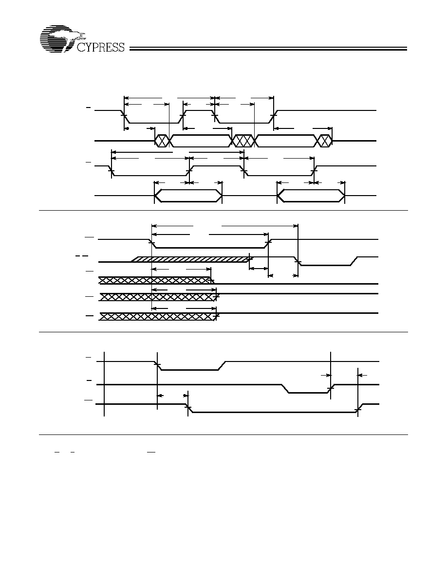
Asynchronous Read and Write
C460A≠7
DATA VALID
DATA VALID
DATA VALID
DATA VALID
t
SD
t
HD
t
RC
t
PR
t
A
t
RR
t
A
t
LZR
t
DVR
t
HZR
t
WC
t
PW
t
WR
R
Q
0
-
Q
8
W
D
0
-
D
8
t
SD
t
HD
t
PW
Master Reset
MR
R, W
HF
FF
EF
t
MRSC
t
PMR
t
EFL
t
HFH
t
FFH
t
RPW
t
WPW
t
RMR
C460A≠8
[10]
[9]
HALF FULL+1
HALF FULL
HALF FULL
W
R
HF
t
WHF
t
RHF
Half Full Flag
C460A≠9