Äîêóìåíòàöèÿ è îïèñàíèÿ www.docs.chipfind.ru
September 8, 2004
© Cypress MicroSystems, Inc. 2004 -- Document No. 38-12028 Rev. *B
1
PSoCTM Mixed-Signal Array
Final Data Sheet
CY8C24123A,
CY8C24223A, and CY8C24423A
PSoCTM Functional Overview
The PSoCTM family consists of many Mixed-Signal Array with
On-Chip Controller devices. These devices are designed to
replace multiple traditional MCU-based system components
with one, low cost single-chip programmable device. PSoC
devices include configurable blocks of analog and digital logic,
as well as programmable interconnects. This architecture
allows the user to create customized peripheral configurations
that match the requirements of each individual application.
Additionally, a fast CPU, Flash program memory, SRAM data
memory, and configurable IO are included in a range of conve-
nient pinouts and packages.
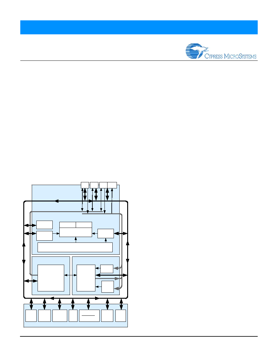
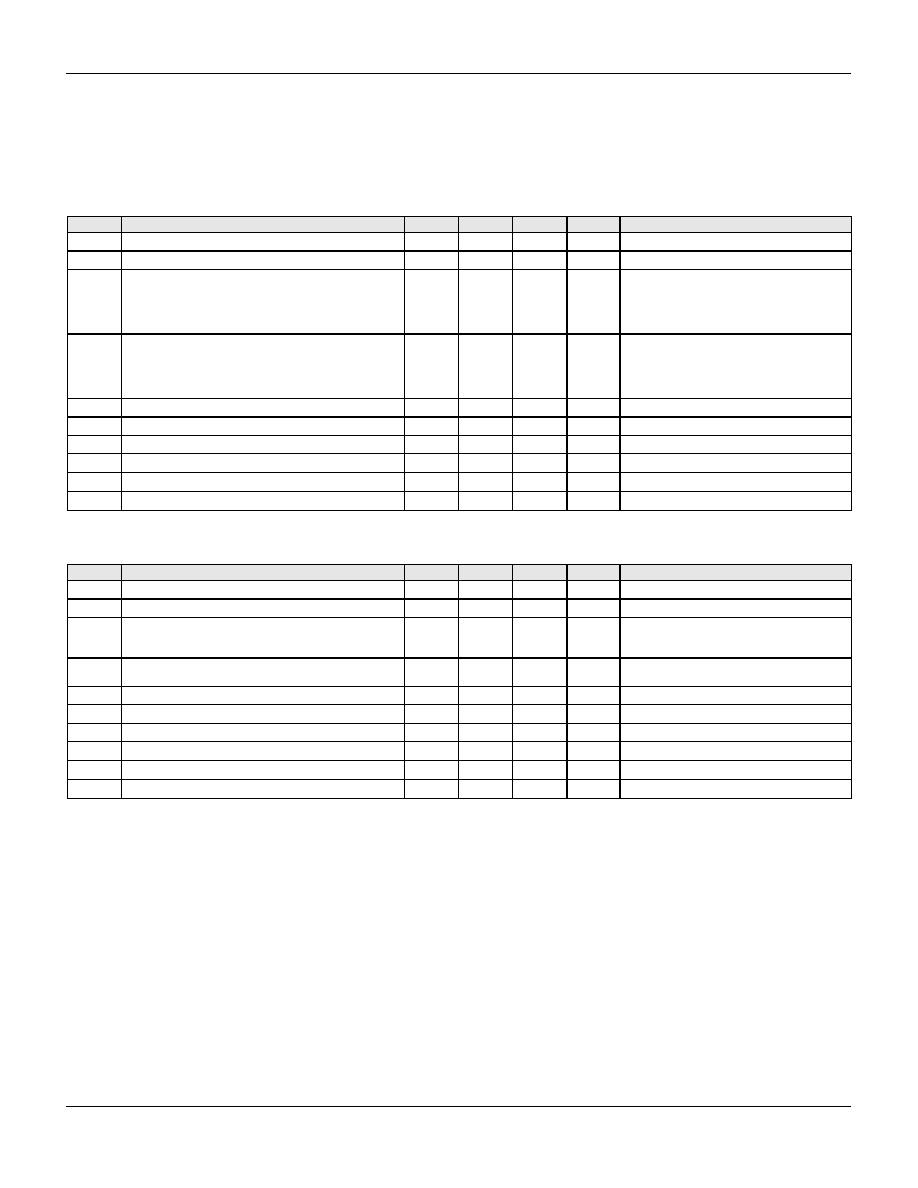
The PSoC architecture, as illustrated on the left, is comprised of
four main areas: PSoC Core, Digital System, Analog System,
and System Resources. Configurable global busing allows all
the device resources to be combined into a complete custom
system. The PSoC CY8C24x23A family can have up to three IO
ports that connect to the global digital and analog interconnects,
providing access to 4 digital blocks and 6 analog blocks.
The PSoC Core
The PSoC Core is a powerful engine that supports a rich fea-
ture set. The core includes a CPU, memory, clocks, and config-
urable GPIO (General Purpose IO).
The M8C CPU core is a powerful processor with speeds up to
24 MHz, providing a four MIPS 8-bit Harvard architecture micro-
Features
Powerful Harvard Architecture Processor
M8C Processor Speeds to 24 MHz
8x8 Multiply, 32-Bit Accumulate
Low Power at High Speed
2.4 to 5.25 V Operating Voltage
Operating Voltages Down to 1.0V Using On-
Chip Switch Mode Pump (SMP)
Industrial Temperature Range: -40°C to +85°C
Advanced Peripherals (PSoC Blocks)
6 Rail-to-Rail Analog PSoC Blocks Provide:
- Up to 14-Bit ADCs
- Up to 9-Bit DACs
- Programmable Gain Amplifiers
- Programmable Filters and Comparators
4 Digital PSoC Blocks Provide:
- 8- to 32-Bit Timers, Counters, and PWMs
- CRC and PRS Modules
- Full-Duplex UART
- Multiple SPI
TM
Masters or Slaves
- Connectable to all GPIO Pins
Complex Peripherals by Combining Blocks
Precision, Programmable Clocking
Internal ±2.5% 24/48 MHz Oscillator
High-Accuracy 24 MHz with Optional 32 kHz
Crystal and PLL
Optional External Oscillator, up to 24 MHz
Internal Oscillator for Watchdog and Sleep
Flexible On-Chip Memory
4K Bytes Flash Program Storage 50,000
Erase/Write Cycles
256 Bytes SRAM Data Storage
In-System Serial Programming (ISSP
TM
)
Partial Flash Updates
Flexible Protection Modes
EEPROM Emulation in Flash
Programmable Pin Configurations
25 mA Sink on all GPIO
Pull up, Pull down, High Z, Strong, or Open
Drain Drive Modes on all GPIO
Up to 10 Analog Inputs on GPIO
Two 30 mA Analog Outputs on GPIO
Configurable Interrupt on all GPIO
New CY8C24x23A PSoC Device
Derived from the CY8C24x23 Device
Low Power and Low Voltage (2.4V)
Additional System Resources
I
2
C
TM
Slave, Master, and Multi-Master to
400 kHz
Watchdog and Sleep Timers
User-Configurable Low Voltage Detection
Integrated Supervisory Circuit
On-Chip Precision Voltage Reference
Complete Development Tools
Free Development Software
(PSoCTM Designer)
Full-Featured, In-Circuit Emulator and
Programmer
Full Speed Emulation
Complex Breakpoint Structure
128K Bytes Trace Memory
DIGITAL SYSTEM
SRAM
256 Bytes
Interrupt
Controller
Sleep and
Watchdog
Multiple Clock Sources
(Includes IMO, ILO, PLL, and ECO)
Global Digital Interconnect
Global Analog Interconnect
PSoC CORE
CPU Core (M8C)
SROM
Flash 4K
Digital
Block
Array
Multiply
Accum.
Switch
Mode
Pump
Internal
Voltage
Ref.
Digital
Clocks
POR and LVD
System Resets
Decimator
SYSTEM RESOURCES
ANALOG SYSTEM
Analog
Ref
Analog
Input
Muxing
I
2
C
(1 Row,
4 Blocks)
Port 2
Port 1
Port 0
Analog
Drivers
System Bus
Analog
Block
Array
(2 Columns,
6 Blocks)
September 8, 2004
Document No. 38-12028 Rev. *B
2
CY8C24x23A Final Data Sheet
PSoCTM Overview
processor. The CPU utilizes an interrupt controller with 11 vec-
tors, to simplify programming of real time embedded events.
Program execution is timed and protected using the included
Sleep and Watch Dog Timers (WDT).
Memory encompasses 4 KB of Flash for program storage, 256
bytes of SRAM for data storage, and up to 2 KB of EEPROM
emulated using the Flash. Program Flash utilizes four protec-
tion levels on blocks of 64 bytes, allowing customized software
IP protection.
The PSoC device incorporates flexible internal clock genera-
tors, including a 24 MHz IMO (internal main oscillator) accurate
to 2.5% over temperature and voltage. The 24 MHz IMO can
also be doubled to 48 MHz for use by the digital system. A low
power 32 kHz ILO (internal low speed oscillator) is provided for
the Sleep timer and WDT. If crystal accuracy is desired, the
ECO (32.768 kHz external crystal oscillator) is available for use
as a Real Time Clock (RTC) and can optionally generate a crys-
tal-accurate 24 MHz system clock using a PLL. The clocks,
together with programmable clock dividers (as a System
Resource), provide the flexibility to integrate almost any timing
requirement into the PSoC device.
PSoC GPIOs provide connection to the CPU, digital and analog
resources of the device. Each pin's drive mode may be selected
from eight options, allowing great flexibility in external interfac-
ing. Every pin also has the capability to generate a system inter-
rupt on high level, low level, and change from last read.
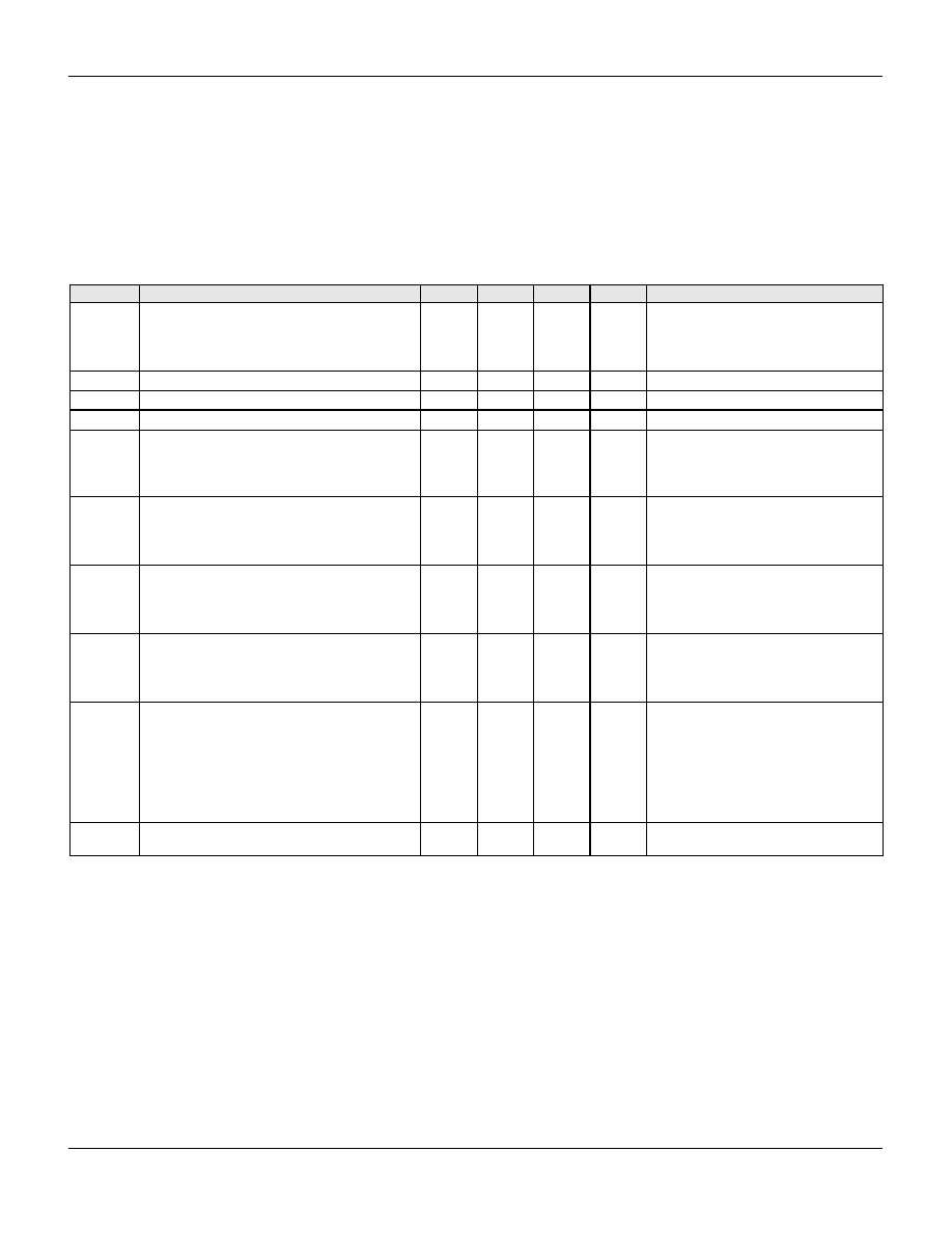
The Digital System
The Digital System is composed of 4 digital PSoC blocks. Each
block is an 8-bit resource that can be used alone or combined
with other blocks to form 8, 16, 24, and 32-bit peripherals, which
are called user module references.
Digital System Block Diagram
Digital peripheral configurations include those listed below.
PWMs (8 to 32 bit)
PWMs with Dead band (8 to 24 bit)
Counters (8 to 32 bit)
Timers (8 to 32 bit)
UART 8 bit with selectable parity
SPI master and slave
I2C slave and multi-master (1 available as a System
Resource)
Cyclical Redundancy Checker/Generator (8 to 32 bit)
IrDA (up to 1)
Pseudo Random Sequence Generators (8 to 32 bit)
The digital blocks can be connected to any GPIO through a
series of global buses that can route any signal to any pin. The
buses also allow for signal multiplexing and for performing logic
operations. This configurability frees your designs from the con-
straints of a fixed peripheral controller.
Digital blocks are provided in rows of four, where the number of
blocks varies by PSoC device family. This allows you the opti-
mum choice of system resources for your application. Family
resources are shown in the table titled
"PSoC Device Charac-
teristics" on page 3
.
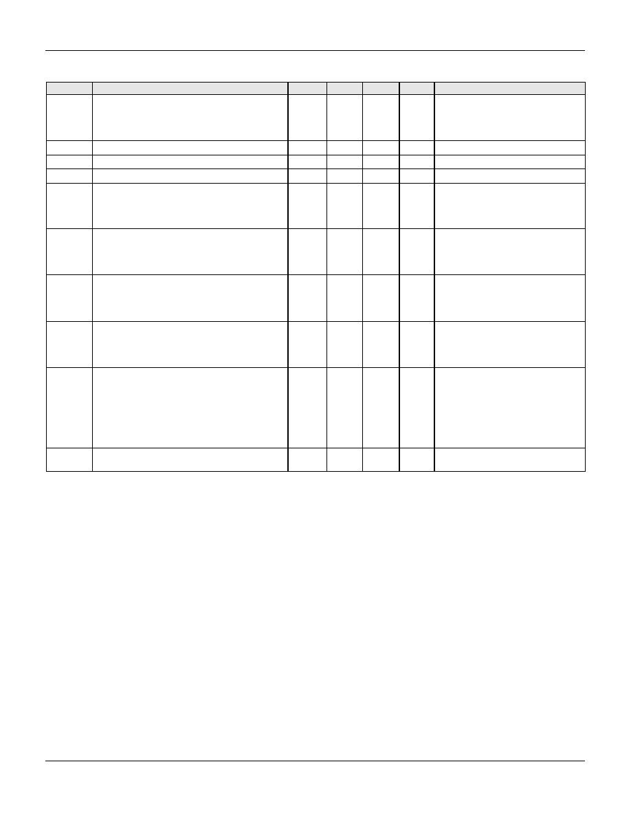
The Analog System
The Analog System is composed of 6 configurable blocks, each
comprised of an opamp circuit allowing the creation of complex
analog signal flows. Analog peripherals are very flexible and
can be customized to support specific application requirements.
Some of the more common PSoC analog functions (most avail-
able as user modules) are listed below.
Analog-to-digital converters (up to 2, with 6- to 14-bit resolu-
tion, selectable as Incremental, Delta Sigma, and SAR)
Filters (2 and 4 pole band-pass, low-pass, and notch)
Amplifiers (up to 2, with selectable gain to 48x)
Instrumentation amplifiers (1 with selectable gain to 93x)
Comparators (up to 2, with 16 selectable thresholds)
DACs (up to 2, with 6- to 9-bit resolution)
Multiplying DACs (up to 2, with 6- to 9-bit resolution)
High current output drivers (two with 30 mA drive as a Core
Resource)
1.3V reference (as a System Resource)
DTMF dialer
Modulators
Correlators
Peak detectors
Many other topologies possible
DIGITAL SYSTEM
To System Bus
Digital Clocks
From Core
Digital PSoC Block Array
To Analog
System
8
Row
I
npu
t
Conf
i
gur
at
i
o
n
Row
Out
put
C
onf
i
gur
at
i
o
n
8
8
8
Row 0
DBB00
DBB01
DCB02
DCB03
4
4
GIE[7:0]
GIO[7:0]
GOE[7:0]
GOO[7:0]
Global Digital
Interconnect
Port 2
Port 1
Port 0
September 8, 2004
Document No. 38-12028 Rev. *B
3
CY8C24x23A Final Data Sheet
PSoCTM Overview
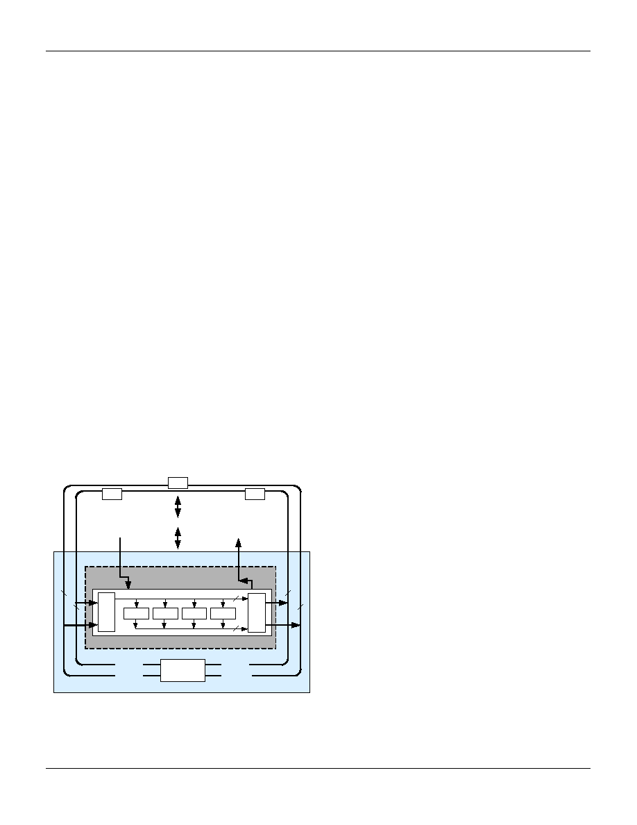
Analog blocks are arranged in a column of three, which
includes one CT (Continuous Time) and two SC (Switched
Capacitor) blocks, as shown in the figure below.
Analog System Block Diagram
Additional System Resources
System Resources, some of which have been previously listed,
provide additional capability useful to complete systems. Addi-
tional resources include a multiplier, decimator, switch mode
pump, low voltage detection, and power on reset. Brief state-
ments describing the merits of each system resource are pre-
sented below.
Digital clock dividers provide three customizable clock fre-
quencies for use in applications. The clocks can be routed to
both the digital and analog systems. Additional clocks can be
generated using digital PSoC blocks as clock dividers.
A multiply accumulate (MAC) provides a fast 8-bit multiplier
with 32-bit accumulate, to assist in both general math as well
as digital filters.
The decimator provides a custom hardware filter for digital
signal processing applications including the creation of Delta
Sigma ADCs.
The I2C module provides 100 and 400 kHz communication
over two wires. Slave, master, and multi-master modes are
all supported.
Low Voltage Detection (LVD) interrupts can signal the appli-
cation of falling voltage levels, while the advanced POR
(Power On Reset) circuit eliminates the need for a system
supervisor.
An internal 1.3V reference provides an absolute reference for
the analog system, including ADCs and DACs.
An integrated switch mode pump (SMP) generates normal
operating voltages from a single 1.2V battery cell, providing a
low cost boost converter.
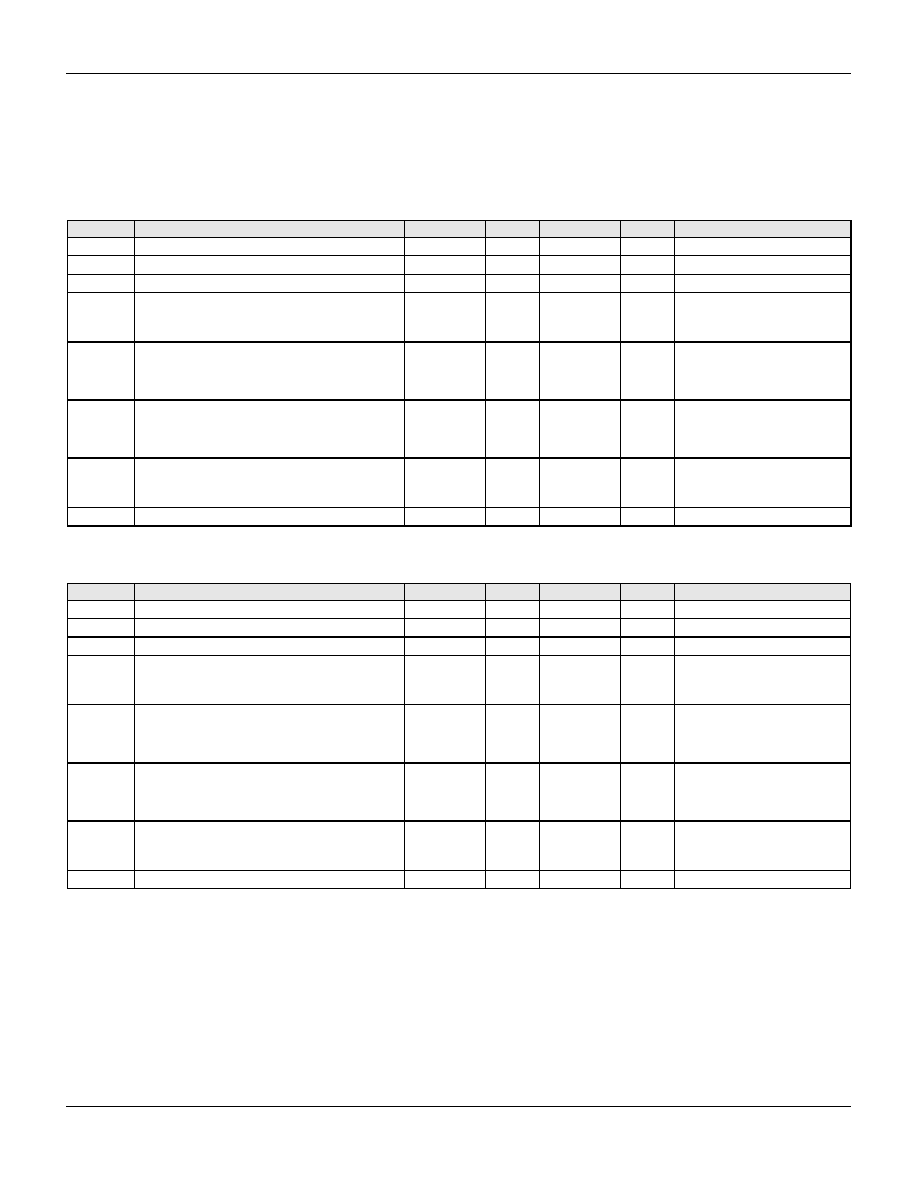
PSoC Device Characteristics
Depending on your PSoC device characteristics, the digital and
analog systems can have 16, 8, or 4 digital blocks and 12, 6, or
3 analog blocks. The following table lists the resources
available for specific PSoC device groups. The PSoC device
covered by this data sheet is shown in the next to the last row of
the table.
ACB00
ACB01
Block Array
Array Input Configuration
ACI1[1:0]
ASD20
ACI0[1:0]
P0[6]
P0[4]
P0[2]
P0[0]
P2[2]
P2[0]
P2[6]
P2[4]
Re
fI
n
AG
NDI
n
P0[7]
P0[5]
P0[3]
P0[1]
P2[3]
P2[1]
Reference
Generators
AGNDIn
RefIn
Bandgap
RefHi
RefLo
AGND
ASD11
ASC21
ASC10
Interface to
Digital System
M8C Interface (Address Bus, Data Bus, Etc.)
Analog Reference
PSoC Device Characteristics
PSoC Device
Group
Di
g
i
t
a
l IO
(m
ax
)
Dig
i
t
a
l
Ro
w
s
Di
g
i
t
a
l Blo
c
k
s
A
n
al
og
I
n
pu
t
s
An
a
l
o
g
Ou
tp
u
t
s
An
a
l
o
g
Co
lu
m
n
s
A
n
alo
g
B
l
oc
ks
Am
o
u
n
t
o
f
SRAM
A
m
ou
nt
o
f
F
l
a
s
h
CY8C29x66
64
4
16
12
4
4
12
2 KB
32 KB
CY8C27x43
44
2
8
12
4
4
12
256 Bytes
16 KB
CY8C24x23
24
1
4
12
2
2
6
256 Bytes
4 KB
CY8C24x23A
24
1
4
12
2
2
6
256 Bytes
4 KB
CY8C22x13
16
1
4
8
1
1
3
256 Bytes
2 KB
CY8C21x34
28
1
4
28
0
2
4
a
a. Limited analog functionality.
512 Bytes
8 KB
CY8C21x23
16
1
4
8
0
2
4
a
256 Bytes
4 KB
September 8, 2004
Document No. 38-12028 Rev. *B
4
CY8C24x23A Final Data Sheet
PSoCTM Overview
Getting Started
The quickest path to understanding the PSoC silicon is by read-
ing this data sheet and using the PSoC Designer Integrated
Development Environment (IDE). This data sheet is an over-
view of the PSoC integrated circuit and presents specific pin,
register, and electrical specifications. For in-depth information,
along with detailed programming information, reference the
PSoCTM Mixed Signal Array Technical Reference Manual.
For up-to-date Ordering, Packaging, and Electrical Specification
information, reference the latest PSoC device data sheets on
the web at
http://www.cypress.com/psoc.
Development Kits
Development Kits are available from the following distributors:
Digi-Key, Avnet, Arrow, and Future. The Cypress Online Store
at
http://www.onfulfillment.com/cypressstore/
contains develop-
ment kits, C compilers, and all accessories for PSoC develop-
ment. Click on PSoC (Programmable System-on-Chip) to view
a current list of available items.
Tele-Training
Free PSoC "Tele-training" is available for beginners and taught
by a live marketing or application engineer over the phone. Five
training classes are available to accelerate the learning curve
including introduction, designing, debugging, advanced design,
advanced analog, as well as application-specific classes cover-
ing topics like PSoC and the LIN bus. For days and times of the
tele-training, see
http://www.cypress.com/support/training.cfm
.
Consultants
Certified PSoC Consultants offer everything from technical
assistance to completed PSoC designs. To contact or become a
PSoC Consultant, go to the following Cypress support web site:
http://www.cypress.com/support/cypros.cfm
.
Technical Support
PSoC application engineers take pride in fast and accurate
response. They can be reached with a 4-hour guaranteed
response at
http://www.cypress.com/support/login.cfm
.
Application Notes
A long list of application notes will assist you in every aspect of
your design effort. To locate the PSoC application notes, go to
http://www.cypress.com/design/results.cfm
.
Development Tools
The Cypress MicroSystems PSoC Designer is a Microsoft
®
Windows-based, integrated development environment for the
Programmable System-on-Chip (PSoC) devices. The PSoC
Designer IDE and application runs on Windows NT 4.0, Win-
dows 2000, Windows Millennium (Me), or Windows XP. (Refer-
ence the PSoC Designer Functional Flow diagram below.)
PSoC Designer helps the customer to select an operating con-
figuration for the PSoC, write application code that uses the
PSoC, and debug the application. This system provides design
database management by project, an integrated debugger with
In-Circuit Emulator, in-system programming support, and the
CYASM macro assembler for the CPUs.
PSoC Designer also supports a high-level C language compiler
developed specifically for the devices in the family.
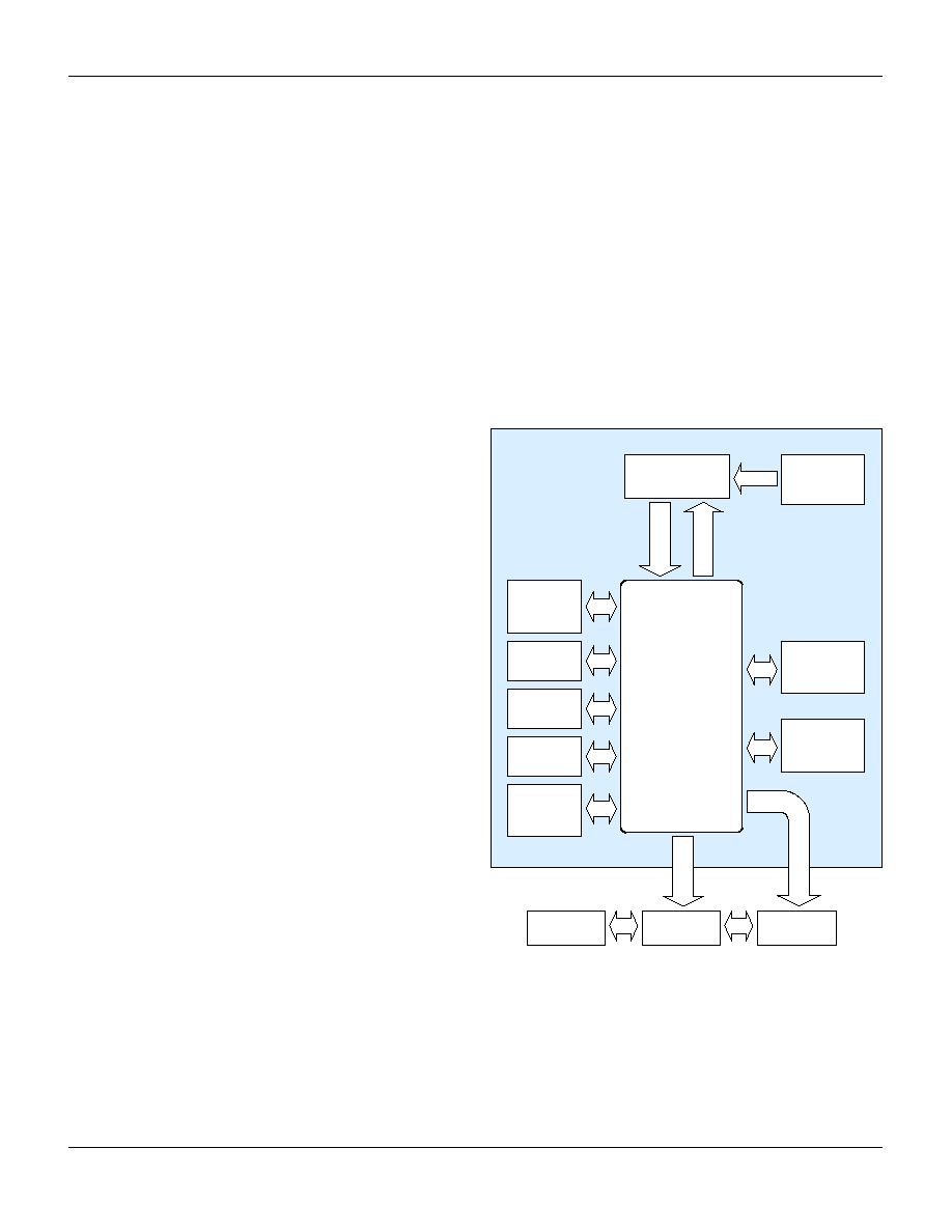
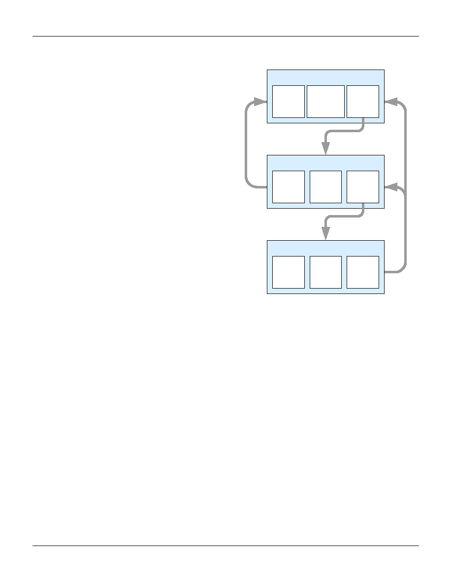
PSoC Designer Subsystems
Co
mmands
Res
u
l
t
s
PSoC
TM
Designer
Core
Engine
PSoC
Configuration
Sheet
Manufacturing
Information
File
Device
Database
Importable
Design
Database
Device
Programmer
Graphical Designer
Interface
Context
Sensitive
Help
Emulation
Pod
In-Circuit
Emulator
Project
Database
Application
Database
User
Modules
Library
PSoC
TM
Designer

September 8, 2004
Document No. 38-12028 Rev. *B
5
CY8C24x23A Final Data Sheet
PSoCTM Overview
PSoC Designer Software Subsystems
Device Editor
The Device Editor subsystem allows the user to select different
onboard analog and digital components called user modules
using the PSoC blocks. Examples of user modules are ADCs,
DACs, Amplifiers, and Filters.
The device editor also supports easy development of multiple
configurations and dynamic reconfiguration. Dynamic configu-
ration allows for changing configurations at run time.
PSoC Designer sets up power-on initialization tables for
selected PSoC block configurations and creates source code
for an application framework. The framework contains software
to operate the selected components and, if the project uses
more than one operating configuration, contains routines to
switch between different sets of PSoC block configurations at
run time. PSoC Designer can print out a configuration sheet for
a given project configuration for use during application pro-
gramming in conjunction with the Device Data Sheet. Once the
framework is generated, the user can add application-specific
code to flesh out the framework. It's also possible to change the
selected components and regenerate the framework.
Design Browser
The Design Browser allows users to select and import precon-
figured designs into the user's project. Users can easily browse
a catalog of preconfigured designs to facilitate time-to-design.
Examples provided in the tools include a 300-baud modem, LIN
Bus master and slave, fan controller, and magnetic card reader.
Application Editor
In the Application Editor you can edit your C language and
Assembly language source code. You can also assemble, com-
pile, link, and build.
Assembler. The macro assembler allows the assembly code
to be merged seamlessly with C code. The link libraries auto-
matically use absolute addressing or can be compiled in relative
mode, and linked with other software modules to get absolute
addressing.
C Language Compiler. A C language compiler is available
that supports Cypress MicroSystems' PSoC family devices.
Even if you have never worked in the C language before, the
product quickly allows you to create complete C programs for
the PSoC family devices.
The embedded, optimizing C compiler provides all the features
of C tailored to the PSoC architecture. It comes complete with
embedded libraries providing port and bus operations, standard
keypad and display support, and extended math functionality.
Debugger
The PSoC Designer Debugger subsystem provides hardware
in-circuit emulation, allowing the designer to test the program in
a physical system while providing an internal view of the PSoC
device. Debugger commands allow the designer to read and
program and read and write data memory, read and write IO
registers, read and write CPU registers, set and clear break-
points, and provide program run, halt, and step control. The
debugger also allows the designer to create a trace buffer of
registers and memory locations of interest.
Online Help System
The online help system displays online, context-sensitive help
for the user. Designed for procedural and quick reference, each
functional subsystem has its own context-sensitive help. This
system also provides tutorials and links to FAQs and an Online
Support Forum to aid the designer in getting started.
Hardware Tools
In-Circuit Emulator
A low cost, high functionality ICE (In-Circuit Emulator) is avail-
able for development support. This hardware has the capability
to program single devices.
The emulator consists of a base unit that connects to the PC by
way of the parallel or USB port. The base unit is universal and
will operate with all PSoC devices. Emulation pods for each
device family are available separately. The emulation pod takes
the place of the PSoC device in the target board and performs
full speed (24 MHz) operation.
September 8, 2004
Document No. 38-12028 Rev. *B
6
CY8C24x23A Final Data Sheet
PSoCTM Overview
User Module Development Process
The development process for the PSoC device differs from that
of a traditional fixed function microprocessor. The configurable
analog and digital hardware blocks give the PSoC architecture
a unique flexibility that pays dividends in managing specification
change during development and by lowering inventory costs.
These configurable resources, called PSoC Blocks, have the
ability to implement a wide variety of user-selectable functions.
Each block has several registers that determine its function and
connectivity to other blocks, multiplexers, buses and to the IO
pins. Iterative development cycles permit you to adapt the hard-
ware as well as the software. This substantially lowers the risk
of having to select a different part to meet the final design
requirements.
To speed the development process, the PSoC Designer Inte-
grated Development Environment (IDE) provides a library of
pre-built, pre-tested hardware peripheral functions, called "User
Modules." User modules make selecting and implementing
peripheral devices simple, and come in analog, digital, and
mixed signal varieties. The standard User Module library con-
tains over 50 common peripherals such as ADCs, DACs Tim-
ers, Counters, UARTs, and other not-so common peripherals
such as DTMF Generators and Bi-Quad analog filter sections.
Each user module establishes the basic register settings that
implement the selected function. It also provides parameters
that allow you to tailor its precise configuration to your particular
application. For example, a Pulse Width Modulator User Mod-
ule configures one or more digital PSoC blocks, one for each 8
bits of resolution. The user module parameters permit you to
establish the pulse width and duty cycle. User modules also
provide tested software to cut your development time. The user
module application programming interface (API) provides high-
level functions to control and respond to hardware events at
run-time. The API also provides optional interrupt service rou-
tines that you can adapt as needed.
The API functions are documented in user module data sheets
that are viewed directly in the PSoC Designer IDE. These data
sheets explain the internal operation of the user module and
provide performance specifications. Each data sheet describes
the use of each user module parameter and documents the set-
ting of each register controlled by the user module.
The development process starts when you open a new project
and bring up the Device Editor, a graphical user interface (GUI)
for configuring the hardware. You pick the user modules you
need for your project and map them onto the PSoC blocks with
point-and-click simplicity. Next, you build signal chains by inter-
connecting user modules to each other and the IO pins. At this
stage, you also configure the clock source connections and
enter parameter values directly or by selecting values from
drop-down menus. When you are ready to test the hardware
configuration or move on to developing code for the project, you
perform the "Generate Application" step. This causes PSoC
Designer to generate source code that automatically configures
the device to your specification and provides the high-level user
module API functions.
User Module and Source Code Development Flows
The next step is to write your main program, and any sub-rou-
tines using PSoC Designer's Application Editor subsystem.
The Application Editor includes a Project Manager that allows
you to open the project source code files (including all gener-
ated code files) from a hierarchal view. The source code editor
provides syntax coloring and advanced edit features for both C
and assembly language. File search capabilities include simple
string searches and recursive "grep-style" patterns. A single
mouse click invokes the Build Manager. It employs a profes-
sional-strength "makefile" system to automatically analyze all
file dependencies and run the compiler and assembler as nec-
essary. Project-level options control optimization strategies
used by the compiler and linker. Syntax errors are displayed in
a console window. Double clicking the error message takes you
directly to the offending line of source code. When all is correct,
the linker builds a HEX file image suitable for programming.
The last step in the development process takes place inside the
PSoC Designer's Debugger subsystem. The Debugger down-
loads the HEX image to the In-Circuit Emulator (ICE) where it
runs at full speed. Debugger capabilities rival those of systems
costing many times more. In addition to traditional single-step,
run-to-breakpoint and watch-variable features, the Debugger
provides a large trace buffer and allows you define complex
breakpoint events that include monitoring address and data bus
values, memory locations and external signals.
Debugger
Interface
to ICE
Application Editor
Device Editor
Project
Manager
Source
Code
Editor
Storage
Inspector
User
Module
Selection
Placement
and
Parameter-
ization
Generate
Application
Build
All
Event &
Breakpoint
Manager
Build
Manager
Source
Code
Generator
September 8, 2004
Document No. 38-12028 Rev. *B
7
CY8C24x23A Final Data Sheet
PSoCTM Overview
Document Conventions
Acronyms Used
The following table lists the acronyms that are used in this doc-
ument.
Units of Measure
A units of measure table is located in the Electrical Specifica-
tions section.
Table 3-1 on page 15
lists all the abbreviations
used to measure the PSoC devices.
Numeric Naming
Hexidecimal numbers are represented with all letters in upper-
case with an appended lowercase `h' (for example, `14h' or
`3Ah'). Hexidecimal numbers may also be represented by a `0x'
prefix, the C coding convention. Binary numbers have an
appended lowercase `b' (e.g., 01010100b' or `01000011b').
Numbers not indicated by an `h' or `b' are decimal.
Table of Contents
For an in depth discussion and more information on your PSoC
device, obtain the PSoC Mixed Signal Array Technical Refer-
ence Manual. This document encompasses and is organized
into the following chapters and sections.
1.
Pin Information ............................................................. 8
1.1
Pinouts ................................................................... 8
1.1.1
8-Pin Part Pinout ........................................ 8
1.1.2
20-Pin Part Pinout ...................................... 9
1.1.3
28-Pin Part Pinout .................................... 10
1.1.4
32-Pin Part Pinout .................................... 11
2.
Register Reference ..................................................... 12
2.1
Register Conventions ........................................... 12
2.1.1
Abbreviations Used .................................. 12
2.2
Register Mapping Tables ..................................... 12
3.
Electrical Specifications ............................................ 15
3.1
Absolute Maximum Ratings ................................ 16
3.2
Operating Temperature ....................................... 16
3.3
DC Electrical Characteristics ................................ 17
3.3.1
DC Chip-Level Specifications ................... 17
3.3.2
DC General Purpose IO Specifications .... 18
3.3.3
DC Operational Amplifier Specifications ... 19
3.3.4
DC Analog Output Buffer Specifications ... 22
3.3.5
DC Switch Mode Pump Specifications ..... 24
3.3.6
DC Analog Reference Specifications ....... 25
3.3.7
DC Analog PSoC Block Specifications ..... 26
3.3.8
DC POR, SMP, and LVD Specifications ... 27
3.3.9
DC Programming Specifications ............... 28
3.4
AC Electrical Characteristics ................................ 29
3.4.1
AC Chip-Level Specifications ................... 29
3.4.2
AC General Purpose IO Specifications .... 32
3.4.3
AC Operational Amplifier Specifications ... 33
3.4.4
AC Digital Block Specifications ................. 34
3.4.5
AC Analog Output Buffer Specifications ... 36
3.4.6
AC External Clock Specifications ............. 37
3.4.7
AC Programming Specifications ............... 38
3.4.8
AC I2C Specifications ............................... 39
4.
Packaging Information ............................................... 40
4.1
Packaging Dimensions ......................................... 40
4.2
Thermal Impedances .......................................... 45
4.3
Capacitance on Crystal Pins ............................... 45
5.
Ordering Information .................................................. 46
5.1
Ordering Code Definitions .................................... 46
6.
Sales and Company Information ............................... 47
6.1
Revision History ................................................... 47
6.2
Copyrights and Code Protection .......................... 47
Acronym
Description
AC
alternating current
ADC
analog-to-digital converter
API
application programming interface
CPU
central processing unit
CT
continuous time
DAC
digital-to-analog converter
DC
direct current
ECO
external crystal oscillator
EEPROM
electrically erasable programmable read-only memory
FSR
full scale range
GPIO
general purpose IO
GUI
graphical user interface
HBM
human body model
ICE
in-circuit emulator
ILO
internal low speed oscillator
IMO
internal main oscillator
IO
input/output
IPOR
imprecise power on reset
LSb
least-significant bit
LVD
low voltage detect
MSb
most-significant bit
PC
program counter
PLL
phase-locked loop
POR
power on reset
PPOR
precision power on reset
PSoCTM
Programmable System-on-ChipTM
PWM
pulse width modulator
SC
switched capacitor
SLIMO
slow IMO
SMP
switch mode pump
SRAM
static random access memory
September 8, 2004
Document No. 38-12028 Rev. *B
8
1.
Pin Information
This chapter describes, lists, and illustrates the CY8C24x23A PSoC device pins and pinout configurations.
1.1
Pinouts
The CY8C24x23A PSoC device is available in a variety of packages which are listed and illustrated in the following tables. Every
port pin (labeled with a "P") is capable of Digital IO. However, Vss, Vdd, SMP, and XRES are not capable of Digital IO.
1.1.1
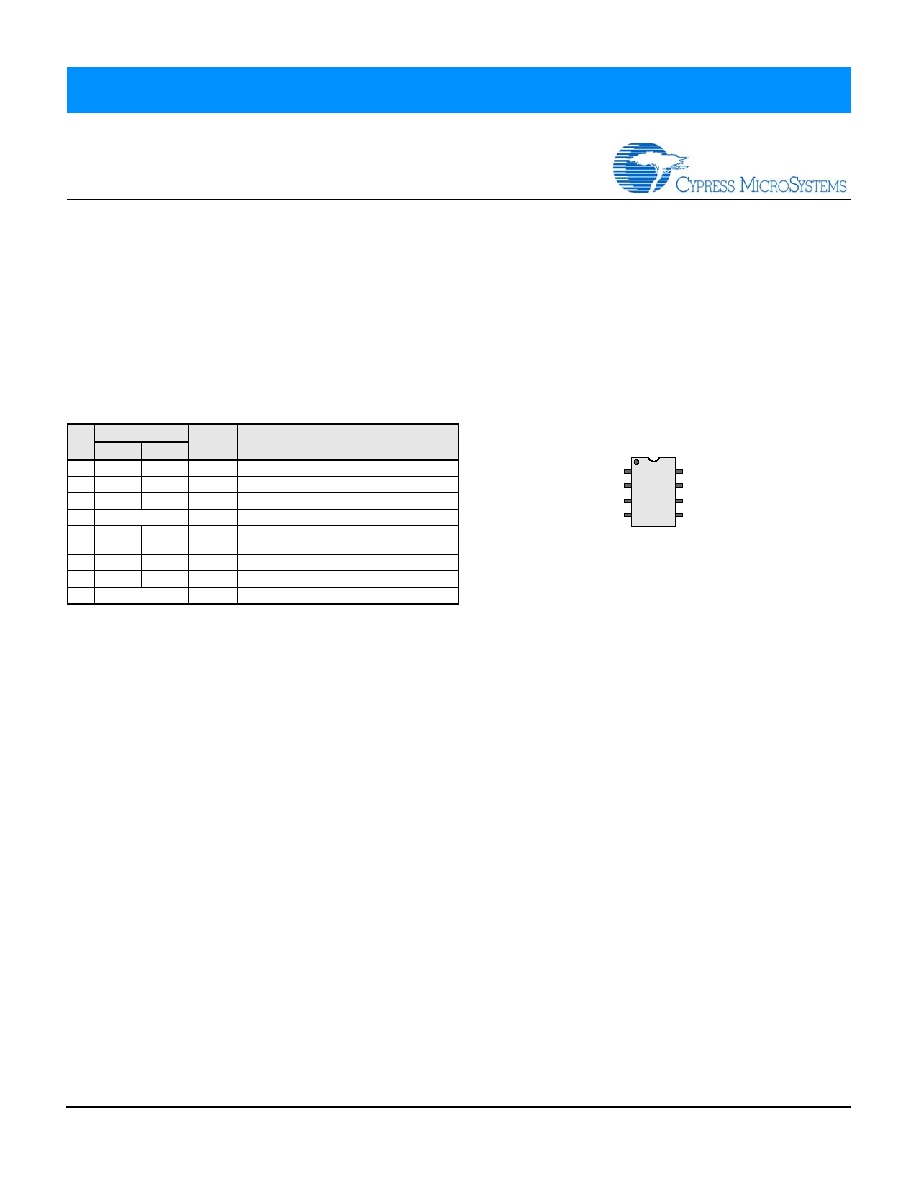
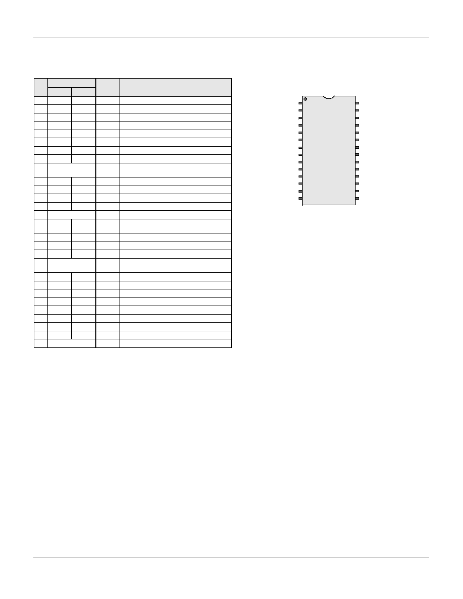
8-Pin Part Pinout
Table 1-1. 8-Pin Part Pinout (PDIP, SOIC)
Pin
No.
Type
Pin
Name
Description
CY8C24123A 8-Pin PSoC Device
Digital
Analog
1
IO
IO
P0[5]
Analog column mux input and column output.
2
IO
IO
P0[3]
Analog column mux input and column output.
3
IO
P1[1]
Crystal Input (XTALin), I2C Serial Clock (SCL)
4
Power
Vss
Ground connection.
5
IO
P1[0]
Crystal Output (XTALout), I2C Serial Data
(SDA)
6
IO
I
P0[2]
Analog column mux input.
7
IO
I
P0[4]
Analog column mux input.
8
Power
Vdd
Supply voltage.
LEGEND
: A = Analog, I = Input, and O = Output.
PDIP
SOIC
1
2
3
4
8
7
6
5
Vdd
P0[4], AI
P0[2], AI
P1[0], XTALout, I2C SDA
AIO, P0[5]
AIO, P0[3]
I2C SCL, XTALin, P1[1]
Vss
September 8, 2004
Document No. 38-12028 Rev. *B
9
CY8C24x23A Final Data Sheet
1. Pin Information
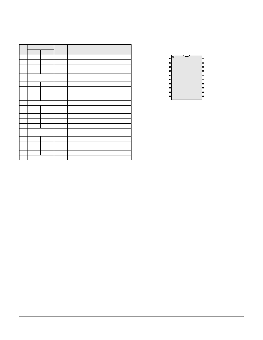
1.1.2
20-Pin Part Pinout
Table 1-2. 20-Pin Part Pinout (PDIP, SSOP, SOIC)
Pin
No.
Type
Pin
Name
Description
CY8C24223A 20-Pin PSoC Device
Digital
Analog
1
IO
I
P0[7]
Analog column mux input.
2
IO
IO
P0[5]
Analog column mux input and column output.
3
IO
IO
P0[3]
Analog column mux input and column output.
4
IO
I
P0[1]
Analog column mux input.
5
Power
SMP
Switch Mode Pump (SMP) connection to
external components required.
6
IO
P1[7]
I2C Serial Clock (SCL)
7
IO
P1[5]
I2C Serial Data (SDA)
8
IO
P1[3]
9
IO
P1[1]
Crystal Input (XTALin), I2C Serial Clock (SCL)
10
Power
Vss
Ground connection.
11
IO
P1[0]
Crystal Output (XTALout), I2C Serial Data
(SDA)
12
IO
P1[2]
13
IO
P1[4]
Optional External Clock Input (EXTCLK)
14
IO
P1[6]
15
Input
XRES
Active high external reset with internal pull
down.
16
IO
I
P0[0]
Analog column mux input.
17
IO
I
P0[2]
Analog column mux input.
18
IO
I
P0[4]
Analog column mux input.
19
IO
I
P0[6]
Analog column mux input.
20
Power
Vdd
Supply voltage.
LEGEND
: A = Analog, I = Input, and O = Output.
AI, P0[7]
AIO, P0[5]
AIO, P0[3]
AI, P0[1]
SMP
I2C SCL, P1[7]
I2C SDA, P1[5]
P1[3]
I2C SCL, XTALin, P1[1]
Vss
PDIP
SSOP
SOIC
20
19
18
17
16
15
14
13
12
11
1
2
3
4
5
6
7
8
9
10
Vdd
P0[6], AI
P0[4], AI
P0[2], AI
P0[0], AI
XRES
P1[6]
P1[4], EXTCLK
P1[2]
P1[0], XTALout, I2C SDA
September 8, 2004
Document No. 38-12028 Rev. *B
10
CY8C24x23A Final Data Sheet
1. Pin Information
1.1.3
28-Pin Part Pinout
Table 1-3. 28-Pin Part Pinout (PDIP, SSOP, SOIC)
Pin
No.
Type
Pin
Name
Description
CY8C24423A 28-Pin PSoC Device
Digital
Analog
1
IO
I
P0[7]
Analog column mux input.
2
IO
IO
P0[5]
Analog column mux input and column output.
3
IO
IO
P0[3]
Analog column mux input and column output.
4
IO
I
P0[1]
Analog column mux input.
5
IO
P2[7]
6
IO
P2[5]
7
IO
I
P2[3]
Direct switched capacitor block input.
8
IO
I
P2[1]
Direct switched capacitor block input.
9
Power
SMP
Switch Mode Pump (SMP) connection to
external components required.
10
IO
P1[7]
I2C Serial Clock (SCL)
11
IO
P1[5]
I2C Serial Data (SDA)
12
IO
P1[3]
13
IO
P1[1]
Crystal Input (XTALin), I2C Serial Clock (SCL)
14
Power
Vss
Ground connection.
15
IO
P1[0]
Crystal Output (XTALout), I2C Serial Data
(SDA)
16
IO
P1[2]
17
IO
P1[4]
Optional External Clock Input (EXTCLK)
18
IO
P1[6]
19
Input
XRES
Active high external reset with internal pull
down.
20
IO
I
P2[0]
Direct switched capacitor block input.
21
IO
I
P2[2]
Direct switched capacitor block input.
22
IO
P2[4]
External Analog Ground (AGND)
23
IO
P2[6]
External Voltage Reference (VRef)
24
IO
I
P0[0]
Analog column mux input.
25
IO
I
P0[2]
Analog column mux input.
26
IO
I
P0[4]
Analog column mux input.
27
IO
I
P0[6]
Analog column mux input.
28
Power
Vdd
Supply voltage.
LEGEND
: A = Analog, I = Input, and O = Output.
AI, P0[7]
AIO, P0[5]
AIO, P0[3]
AI, P0[1]
P2[7]
P2[5]
AI, P2[3]
AI, P2[1]
SMP
I2C SCL, P1[7]
I2C SDA, P1[5]
P1[3]
I2C SCL, XTALin, P1[1]
Vss
Vdd
P0[6], AI
P0[4], AI
P0[2], AI
P0[0], AI
P2[6], External VRef
P2[4], External AGND
P2[2], AI
P2[0], AI
XRES
P1[6]
P1[4], EXTCLK
P1[2]
P1[0], XTALout, I2C SDA
PDIP
SSOP
SOIC
1
2
3
4
5
6
7
8
9
10
11
12
13
14
28
27
26
25
24
23
22
21
20
19
18
17
16
15
September 8, 2004
Document No. 38-12028 Rev. *B
11
CY8C24x23A Final Data Sheet
1. Pin Information
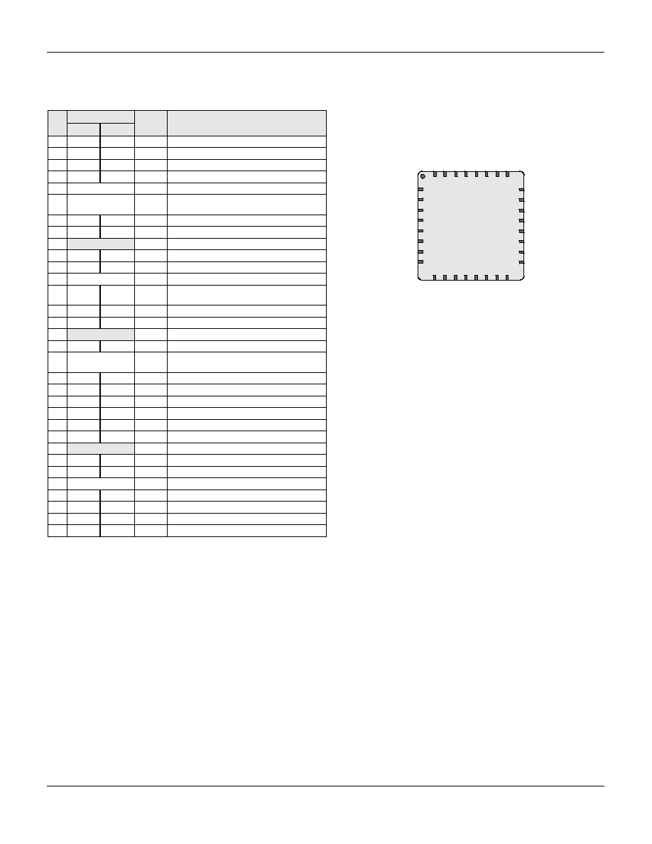
1.1.4
32-Pin Part Pinout
Table 1-4. 32-Pin Part Pinout (MLF*)
Pin
No.
Type
Pin
Name
Description
CY8C24423A 32-Pin PSoC Device
Digital
Analog
1
IO
P2[7]
2
IO
P2[5]
3
IO
I
P2[3]
Direct switched capacitor block input.
4
IO
I
P2[1]
Direct switched capacitor block input.
5
Power
Vss
Ground connection.
6
Power
SMP
Switch Mode Pump (SMP) connection to
external components required.
7
IO
P1[7]
I2C Serial Clock (SCL)
8
IO
P1[5]
I2C Serial Data (SDA)
9
NC
No connection. Do not use.
10
IO
P1[3]
11
IO
P1[1]
Crystal Input (XTALin), I2C Serial Clock (SCL)
12
Power
Vss
Ground connection.
13
IO
P1[0]
Crystal Output (XTALout), I2C Serial Data
(SDA)
14
IO
P1[2]
15
IO
P1[4]
Optional External Clock Input (EXTCLK)
16
NC
No connection. Do not use.
17
IO
P1[6]
18
Input
XRES
Active high external reset with internal pull
down.
19
IO
I
P2[0]
Direct switched capacitor block input.
20
IO
I
P2[2]
Direct switched capacitor block input.
21
IO
P2[4]
External Analog Ground (AGND)
22
IO
P2[6]
External Voltage Reference (VRef)
23
IO
I
P0[0]
Analog column mux input.
24
IO
I
P0[2]
Analog column mux input.
25
NC
No connection. Do not use.
26
IO
I
P0[4]
Analog column mux input.
27
IO
I
P0[6]
Analog column mux input.
28
Power
Vdd
Supply voltage.
29
IO
I
P0[7]
Analog column mux input.
30
IO
IO
P0[5]
Analog column mux input and column output.
31
IO
IO
P0[3]
Analog column mux input and column output.
32
IO
I
P0[1]
Analog column mux input.
LEGEND
: A = Analog, I = Input, and O = Output.
* The MLF package has a center pad that must be connected to ground (Vss).
P2[7]
P2[5]
AI, P2[3]
AI, P2[1]
Vss
SMP
MLF
(Top View)
9
10
11
12
13
14
15
16
1
2
3
4
5
6
7
8
24
23
22
21
20
19
18
17
32
31
30
29
28
27
26
25
P
0
[1],
A
I
P
0
[3],
A
I
O
P
0
[5],
A
I
O
P
0
[7],
A
I
Vd
d
P
0
[6],
A
I
P
0
[4],
A
I
NC
I2C SCL, P1[7]
I2C SDA, P1[5]
P0[2], AI
P0[0], AI
XRES
P1[6]
NC
P1
[
3
]
I2
C S
C
L,
X
T
A
L
in,
P
1
[1
]
Vs
s
I2
C S
D
A
,
X
T
A
L
ou
t,
P
1
[0
]
P1
[
2
]
EX
TCL
K
,
P1
[
4
]
NC
P2[6], External VRef
P2[4], External AGND
P2[2], AI
P2[0], AI
September 8, 2004
Document No. 38-12028 Rev. *B
12
2.
Register Reference
This chapter lists the registers of the CY8C24x23A PSoC device. For detailed register information, reference the PSoCTM Mixed Sig-
nal Array Technical Reference Manual.
2.1
Register Conventions
2.1.1
Abbreviations Used
The register conventions specific to this section are listed in the
following table.
2.2
Register Mapping Tables
The PSoC device has a total register address space of 512
bytes. The register space is referred to as IO space and is
divided into two banks. The XOI bit in the Flag register (CPU_F)
determines which bank the user is currently in. When the XOI
bit is set the user is in bank 1.
Note In the following register mapping tables, blank fields are
reserved and should not be accessed.
Convention
Description
R
Read register or bit(s)
W
Write register or bit(s)
L
Logical register or bit(s)
C
Clearable register or bit(s)
#
Access is bit specific
September 8, 2004
Document No. 38-12028 Rev. *B
13
CY8C24x23A Final Data Sheet
2. Register Reference
Register Map Bank 0 Table: User Space
Na
m
e
Ad
d
r
(0
,H
ex
)
A
c
ces
s
Na
m
e
Ad
d
r
(0
,H
ex
)
A
c
ces
s
Na
m
e
Ad
d
r
(0
,H
ex
)
A
c
ces
s
Na
m
e
Ad
d
r
(0
,H
ex
)
A
c
ces
s
PRT0DR
00
RW
40
ASC10CR0
80
RW
C0
PRT0IE
01
RW
41
ASC10CR1
81
RW
C1
PRT0GS
02
RW
42
ASC10CR2
82
RW
C2
PRT0DM2
03
RW
43
ASC10CR3
83
RW
C3
PRT1DR
04
RW
44
ASD11CR0
84
RW
C4
PRT1IE
05
RW
45
ASD11CR1
85
RW
C5
PRT1GS
06
RW
46
ASD11CR2
86
RW
C6
PRT1DM2
07
RW
47
ASD11CR3
87
RW
C7
PRT2DR
08
RW
48
88
C8
PRT2IE
09
RW
49
89
C9
PRT2GS
0A
RW
4A
8A
CA
PRT2DM2
0B
RW
4B
8B
CB
0C
4C
8C
CC
0D
4D
8D
CD
0E
4E
8E
CE
0F
4F
8F
CF
10
50
ASD20CR0
90
RW
D0
11
51
ASD20CR1
91
RW
D1
12
52
ASD20CR2
92
RW
D2
13
53
ASD20CR3
93
RW
D3
14
54
ASC21CR0
94
RW
D4
15
55
ASC21CR1
95
RW
D5
16
56
ASC21CR2
96
RW
I2C_CFG
D6
RW
17
57
ASC21CR3
97
RW
I2C_SCR
D7
#
18
58
98
I2C_DR
D8
RW
19
59
99
I2C_MSCR
D9
#
1A
5A
9A
INT_CLR0
DA
RW
1B
5B
9B
INT_CLR1
DB
RW
1C
5C
9C
DC
1D
5D
9D
INT_CLR3
DD
RW
1E
5E
9E
INT_MSK3
DE
RW
1F
5F
9F
DF
DBB00DR0
20
#
AMX_IN
60
RW
A0
INT_MSK0
E0
RW
DBB00DR1
21
W
61
A1
INT_MSK1
E1
RW
DBB00DR2
22
RW
62
A2
INT_VC
E2
RC
DBB00CR0
23
#
ARF_CR
63
RW
A3
RES_WDT
E3
W
DBB01DR0
24
#
CMP_CR0
64
#
A4
DEC_DH
E4
RC
DBB01DR1
25
W
ASY_CR
65
#
A5
DEC_DL
E5
RC
DBB01DR2
26
RW
CMP_CR1
66
RW
A6
DEC_CR0
E6
RW
DBB01CR0
27
#
67
A7
DEC_CR1
E7
RW
DCB02DR0
28
#
68
A8
MUL_X
E8
W
DCB02DR1
29
W
69
A9
MUL_Y
E9
W
DCB02DR2
2A
RW
6A
AA
MUL_DH
EA
R
DCB02CR0
2B
#
6B
AB
MUL_DL
EB
R
DCB03DR0
2C
#
6C
AC
ACC_DR1
EC
RW
DCB03DR1
2D
W
6D
AD
ACC_DR0
ED
RW
DCB03DR2
2E
RW
6E
AE
ACC_DR3
EE
RW
DCB03CR0
2F
#
6F
AF
ACC_DR2
EF
RW
30
ACB00CR3
70
RW
RDI0RI
B0
RW
F0
31
ACB00CR0
71
RW
RDI0SYN
B1
RW
F1
32
ACB00CR1
72
RW
RDI0IS
B2
RW
F2
33
ACB00CR2
73
RW
RDI0LT0
B3
RW
F3
34
ACB01CR3
74
RW
RDI0LT1
B4
RW
F4
35
ACB01CR0
75
RW
RDI0RO0
B5
RW
F5
36
ACB01CR1
76
RW
RDI0RO1
B6
RW
F6
37
ACB01CR2
77
RW
B7
CPU_F
F7
RL
38
78
B8
F8
39
79
B9
F9
3A
7A
BA
FA
3B
7B
BB
FB
3C
7C
BC
FC
3D
7D
BD
FD
3E
7E
BE
CPU_SCR1
FE
#
3F
7F
BF
CPU_SCR0
FF
#
Blank fields are Reserved and should not be accessed.
# Access is bit specific.
September 8, 2004
Document No. 38-12028 Rev. *B
14
CY8C24x23A Final Data Sheet
2. Register Reference
Register Map Bank 1 Table: Configuration Space
Na
m
e
Ad
d
r
(1
,
H
ex
)
A
cce
ss
Na
m
e
Ad
d
r
(1
,
H
ex
)
A
cce
ss
Na
m
e
Ad
d
r
(1
,
H
ex
)
A
cce
ss
Na
m
e
Ad
d
r
(1
,
H
ex
)
A
cce
ss
PRT0DM0
00
RW
40
ASC10CR0
80
RW
C0
PRT0DM1
01
RW
41
ASC10CR1
81
RW
C1
PRT0IC0
02
RW
42
ASC10CR2
82
RW
C2
PRT0IC1
03
RW
43
ASC10CR3
83
RW
C3
PRT1DM0
04
RW
44
ASD11CR0
84
RW
C4
PRT1DM1
05
RW
45
ASD11CR1
85
RW
C5
PRT1IC0
06
RW
46
ASD11CR2
86
RW
C6
PRT1IC1
07
RW
47
ASD11CR3
87
RW
C7
PRT2DM0
08
RW
48
88
C8
PRT2DM1
09
RW
49
89
C9
PRT2IC0
0A
RW
4A
8A
CA
PRT2IC1
0B
RW
4B
8B
CB
0C
4C
8C
CC
0D
4D
8D
CD
0E
4E
8E
CE
0F
4F
8F
CF
10
50
ASD20CR0
90
RW
GDI_O_IN
D0
RW
11
51
ASD20CR1
91
RW
GDI_E_IN
D1
RW
12
52
ASD20CR2
92
RW
GDI_O_OU
D2
RW
13
53
ASD20CR3
93
RW
GDI_E_OU
D3
RW
14
54
ASC21CR0
94
RW
D4
15
55
ASC21CR1
95
RW
D5
16
56
ASC21CR2
96
RW
D6
17
57
ASC21CR3
97
RW
D7
18
58
98
D8
19
59
99
D9
1A
5A
9A
DA
1B
5B
9B
DB
1C
5C
9C
DC
1D
5D
9D
OSC_GO_EN
DD
RW
1E
5E
9E
OSC_CR4
DE
RW
1F
5F
9F
OSC_CR3
DF
RW
DBB00FN
20
RW
CLK_CR0
60
RW
A0
OSC_CR0
E0
RW
DBB00IN
21
RW
CLK_CR1
61
RW
A1
OSC_CR1
E1
RW
DBB00OU
22
RW
ABF_CR0
62
RW
A2
OSC_CR2
E2
RW
23
AMD_CR0
63
RW
A3
VLT_CR
E3
RW
DBB01FN
24
RW
64
A4
VLT_CMP
E4
R
DBB01IN
25
RW
65
A5
E5
DBB01OU
26
RW
AMD_CR1
66
RW
A6
E6
27
ALT_CR0
67
RW
A7
E7
DCB02FN
28
RW
68
A8
IMO_TR
E8
W
DCB02IN
29
RW
69
A9
ILO_TR
E9
W
DCB02OU
2A
RW
6A
AA
BDG_TR
EA
RW
2B
6B
AB
ECO_TR
EB
W
DCB03FN
2C
RW
6C
AC
EC
DCB03IN
2D
RW
6D
AD
ED
DCB03OU
2E
RW
6E
AE
EE
2F
6F
AF
EF
30
ACB00CR3
70
RW
RDI0RI
B0
RW
F0
31
ACB00CR0
71
RW
RDI0SYN
B1
RW
F1
32
ACB00CR1
72
RW
RDI0IS
B2
RW
F2
33
ACB00CR2
73
RW
RDI0LT0
B3
RW
F3
34
ACB01CR3
74
RW
RDI0LT1
B4
RW
F4
35
ACB01CR0
75
RW
RDI0RO0
B5
RW
F5
36
ACB01CR1
76
RW
RDI0RO1
B6
RW
F6
37
ACB01CR2
77
RW
B7
CPU_F
F7
RL
38
78
B8
F8
39
79
B9
F9
3A
7A
BA
FA
3B
7B
BB
FB
3C
7C
BC
FC
3D
7D
BD
FD
3E
7E
BE
CPU_SCR1
FE
#
3F
7F
BF
CPU_SCR0
FF
#
Blank fields are Reserved and should not be accessed.
# Access is bit specific.
September 8, 2004
Document No. 38-12028 Rev. *B
15
3.
Electrical Specifications
This chapter presents the DC and AC electrical specifications of the CY8C24x23A PSoC device. For the most up to date electrical
specifications, confirm that you have the most recent data sheet by going to the web at
http://www.cypress.com/psoc.
Specifications are valid for -40
o
C
T
A
85
o
C and T
J
100
o
C, except where noted. Specifications for devices running at greater
than 12 MHz are valid for -40
o
C
T
A
70
o
C and T
J
82
o
C.
Refer to Table 3-20 for the electrical specifications on the internal main oscillator (IMO) using SLIMO mode.
Figure 3-1a. Voltage versus CPU Frequency Figure 3-1b. IMO Frequency Trim Options
The following table lists the units of measure that are used in this chapter.
Table 3-1: Units of Measure
Symbol
Unit of Measure
Symbol
Unit of Measure
o
C
degree Celsius
µ
W
micro watts
dB
decibels
mA
milli-ampere
fF
femto farad
ms
milli-second
Hz
hertz
mV
milli-volts
KB
1024 bytes
nA
nano ampere
Kbit
1024 bits
ns
nanosecond
kHz
kilohertz
nV
nanovolts
k
kilohm
ohm
MHz
megahertz
pA
pico ampere
M
megaohm
pF
pico farad
µ
A
micro ampere
pp
peak-to-peak
µ
F
micro farad
ppm
parts per million
µ
H
micro henry
ps
picosecond
µ
s
microsecond
sps
samples per second
µ
V
micro volts
sigma: one standard deviation
µ
Vrms
micro volts root-mean-square
V
volts
5.25
4.75
3.00
93 kHz
12 MHz
24 MHz
CPU Frequency
Vd
d Vol
t
a
g
e
5.25
4.75
3.00
93 kHz
12 MHz
24 MHz
IMO Frequency
Vd
d Vol
t
a
g
e
3.60
6 MHz
S
L
IM
O Mode
= 0
SLIMO
Mode=0
2.40
SLIMO
Mode=1
SLIMO
Mode=1
SLIMO
Mode=1
2.40
3 MHz
V
ali
d
O
p
er
at
in
g
R
eg
io
n
SLIMO
Mode=1
SLIMO
Mode=0
September 8, 2004
Document No. 38-12028 Rev. *B
16
CY8C24x23A Final Data Sheet
3. Electrical Specifications
3.1
Absolute Maximum Ratings
3.2
Operating Temperature
Table 3-2. Absolute Maximum Ratings
Symbol
Description
Min
Typ
Max
Units
Notes
T
STG
Storage Temperature
-55
+100
o
C
Higher storage temperatures will reduce data
retention time.
T
A
Ambient Temperature with Power Applied
-40
+85
o
C
Vdd
Supply Voltage on Vdd Relative to Vss
-0.5
+6.0
V
V
IO
DC Input Voltage
Vss - 0.5
Vdd + 0.5
V
V
IOZ
DC Voltage Applied to Tri-state
Vss - 0.5
Vdd + 0.5
V
I
MIO
Maximum Current into any Port Pin
-25
+50
mA
ESD
Electro Static Discharge Voltage
2000
V
Human Body Model ESD
LU
Latch-up Current
200
mA
Table 3-3. Operating Temperature
Symbol
Description
Min
Typ
Max
Units
Notes
T
A
Ambient Temperature
-40
+85
o
C
T
J
Junction Temperature
-40
+100
o
C
The temperature rise from ambient to junction is
package specific. See
"Thermal Impedances"
on page 45
. The user must limit the power con-
sumption to comply with this requirement.
September 8, 2004
Document No. 38-12028 Rev. *B
17
CY8C24x23A Final Data Sheet
3. Electrical Specifications
3.3
DC Electrical Characteristics
3.3.1
DC Chip-Level Specifications
The following table lists guaranteed maximum and minimum specifications for the voltage and temperature ranges: 4.75V to 5.25V
and -40
°
C
T
A
85
°
C, 3.0V to 3.6V and -40
°
C
T
A
85
°
C, or 2.4V to 3.0V and -40
°
C
T
A
85
°
C, respectively. Typical parameters
apply to 5V, 3.3V, and 2.7V at 25
°
C and are for design guidance only.
Table 3-4. DC Chip-Level Specifications
Symbol
Description
Min
Typ
Max
Units
Notes
Vdd
Supply Voltage
2.4
5.25
V
See DC POR and LVD specifications,
Table 3-
18 on page 27
.
I
DD
Supply Current
5
8
mA
Conditions are Vdd = 5.0V, T
A
= 25
o
C, CPU = 3
MHz, SYSCLK doubler disabled, VC1 = 1.5
MHz, VC2 = 93.75 kHz, VC3 = 93.75 kHz, ana-
log power = off.
I
DD3
Supply Current
3.3
6.0
mA
Conditions are Vdd = 3.3V, T
A
= 25
o
C, CPU = 3
MHz, SYSCLK doubler disabled, VC1 = 1.5
MHz, VC2 = 93.75 kHz, VC3 = 93.75 kHz, ana-
log power = off.
I
DD27
Supply Current when IMO = 6 MHz using SLIMO mode.
2
4
mA
Conditions are Vdd = 3.3V, T
A
= 25
o
C, CPU =
0.75 MHz, 48 MHz = Disabled, VC1 = 0.375
MHz, VC2 = 23.44 kHz, VC3 = 0.09 kHz, analog
power = off.
I
SB
Sleep (Mode) Current with POR, LVD, Sleep Timer, and
WDT.
a
a. Standby current includes all functions (POR, LVD, WDT, Sleep Time) needed for reliable system operation. This should be compared with devices that have similar functions
enabled.
3
6.5
µ
A
Conditions are with internal slow speed oscilla-
tor, Vdd = 3.3V, -40
o
C
T
A
55
o
C, analog
power = off.
I
SBH
Sleep (Mode) Current with POR, LVD, Sleep Timer, and
WDT at high temperature.
a
4
25
µ
A
Conditions are with internal slow speed oscilla-
tor, Vdd = 3.3V, 55
o
C < T
A
85
o
C, analog
power = off.
I
SBXTL
Sleep (Mode) Current with POR, LVD, Sleep Timer, WDT,
and external crystal.
a
4
7.5
µ
A
Conditions are with properly loaded, 1
µ
W max,
32.768 kHz crystal. Vdd = 3.3V, -40
o
C
T
A
55
o
C, analog power = off.
I
SBXTLH
Sleep (Mode) Current with POR, LVD, Sleep Timer, WDT,
and external crystal at high temperature.
a
5
26
µ
A
Conditions are with properly loaded, 1
µ
W max,
32.768 kHz crystal. Vdd = 3.3 V, 55
o
C < T
A
85
o
C, analog power = off.
V
REF
Reference Voltage (Bandgap)
1.28
1.30
1.33
V
Trimmed for appropriate Vdd. Vdd > 3.0V.
V
REF27
Reference Voltage (Bandgap)
1.16
1.30
1.33
V
Trimmed for appropriate Vdd. Vdd = 2.4V to
3.0V.
September 8, 2004
Document No. 38-12028 Rev. *B
18
CY8C24x23A Final Data Sheet
3. Electrical Specifications
3.3.2
DC General Purpose IO Specifications
The following tables list guaranteed maximum and minimum specifications for the voltage and temperature ranges: 4.75V to 5.25V
and -40
°
C
T
A
85
°
C, 3.0V to 3.6V and -40
°
C
T
A
85
°
C, or 2.4V to 3.0V and -40
°
C
T
A
85
°
C, respectively. Typical parameters
apply to 5V, 3.3V, and 2.7V at 25
°
C and are for design guidance only.
Table 3-5. 5V and 3.3V DC GPIO Specifications
Symbol
Description
Min
Typ
Max
Units
Notes
R
PU
Pull up Resistor
4
5.6
8
k
R
PD
Pull down Resistor
4
5.6
8
k
V
OH
High Output Level
Vdd - 1.0
V
IOH = 10 mA, Vdd = 4.75 to 5.25V (maximum
40 mA on even port pins (for example, P0[2],
P1[4]), maximum 40 mA on odd port pins (for
example, P0[3], P1[5])). 80 mA maximum com-
bined IOH budget.
V
OL
Low Output Level
0.75
V
IOL = 25 mA, Vdd = 4.75 to 5.25V (maximum
100 mA on even port pins (for example, P0[2],
P1[4]), maximum 100 mA on odd port pins (for
example, P0[3], P1[5])). 150 mA maximum com-
bined IOL budget.
V
IL
Input Low Level
0.8
V
Vdd = 3.0 to 5.25
V
IH
Input High Level
2.1
V
Vdd = 3.0 to 5.25
V
H
Input Hysterisis
60
mV
I
IL
Input Leakage (Absolute Value)
1
nA
Gross tested to 1
µ
A.
C
IN
Capacitive Load on Pins as Input
3.5
10
pF
Package and pin dependent. Temp = 25
o
C.
C
OUT
Capacitive Load on Pins as Output
3.5
10
pF
Package and pin dependent. Temp = 25
o
C.
Table 3-6. 2.7V DC GPIO Specifications
Symbol
Description
Min
Typ
Max
Units
Notes
R
PU
Pull up Resistor
4
5.6
8
k
R
PD
Pull down Resistor
4
5.6
8
k
V
OH
High Output Level
Vdd - 0.4
V
IOH = 2 mA (6.25 Typ), Vdd = 2.4 to 3.0V (16
mA maximum, 50 mA Typ combined IOH bud-
get).
V
OL
Low Output Level
0.75
V
IOL = 11.25 mA, Vdd = 2.4 to 3.0V (90 mA max-
imum combined IOL budget).
V
IL
Input Low Level
0.8
V
Vdd = 2.4 to 3.0
V
IH
Input High Level
2.0
V
Vdd = 2.4 to 3.0
V
H
Input Hysteresis
90
mV
I
IL
Input Leakage (Absolute Value)
1
nA
Gross tested to 1
µ
A.
C
IN
Capacitive Load on Pins as Input
3.5
10
pF
Package and pin dependent. Temp = 25
o
C.
C
OUT
Capacitive Load on Pins as Output
3.5
10
pF
Package and pin dependent. Temp = 25
o
C.
September 8, 2004
Document No. 38-12028 Rev. *B
19
CY8C24x23A Final Data Sheet
3. Electrical Specifications
3.3.3
DC Operational Amplifier Specifications
The following tables list guaranteed maximum and minimum specifications for the voltage and temperature ranges: 4.75V to 5.25V
and -40
°
C
T
A
85
°
C, 3.0V to 3.6V and -40
°
C
T
A
85
°
C, or 2.4V to 3.0V and -40
°
C
T
A
85
°
C, respectively. Typical parameters
apply to 5V, 3.3V, and 2.7V at 25
°
C and are for design guidance only.
The Operational Amplifier is a component of both the Analog Continuous Time PSoC blocks and the Analog Switched Cap PSoC
blocks. The guaranteed specifications are measured in the Analog Continuous Time PSoC block. Typical parameters apply to 5V at
25
°
C and are for design guidance only.
Table 3-7. 5V DC Operational Amplifier Specifications
Symbol
Description
Min
Typ
Max
Units
Notes
V
OSOA
Input Offset Voltage (absolute value)
Power = Low, Opamp Bias = High
Power = Medium, Opamp Bias = High
Power = High, Opamp Bias = High
1.6
1.3
1.2
10
8
7.5
mV
mV
mV
TCV
OSOA
Average Input Offset Voltage Drift
7.0
35.0
µ
V/
o
C
I
EBOA
Input Leakage Current (Port 0 Analog Pins)
20
pA
Gross tested to 1
µ
A.
C
INOA
Input Capacitance (Port 0 Analog Pins)
4.5
9.5
pF
Package and pin dependent. Temp = 25
o
C.
V
CMOA
Common Mode Voltage Range
Common Mode Voltage Range (high power or high
opamp bias)
0.0
Vdd
Vdd - 0.5
V
The common-mode input voltage range is mea-
sured through an analog output buffer. The
specification includes the limitations imposed
by the characteristics of the analog output
buffer.
0.5
G
OLOA
Open Loop Gain
Power = Low, Opamp Bias = High
Power = Medium, Opamp Bias = High
Power = High, Opamp Bias = High
60
60
80
dB
Specification is applicable at high power. For all
other bias modes (except high power, high
opamp bias), minimum is 60 dB.
V
OHIGHOA
High Output Voltage Swing (internal signals)
Power = Low, Opamp Bias = High
Power = Medium, Opamp Bias = High
Power = High, Opamp Bias = High
Vdd - 0.2
Vdd - 0.2
Vdd - 0.5
V
V
V
V
OLOWOA
Low Output Voltage Swing (internal signals)
Power = Low, Opamp Bias = High
Power = Medium, Opamp Bias = High
Power = High, Opamp Bias = High
0.2
0.2
0.5
V
V
V
I
SOA
Supply Current (including associated AGND buffer)
Power = Low, Opamp Bias = High
Power = Low, Opamp Bias = High
Power = Medium, Opamp Bias = High
Power = Medium, Opamp Bias = High
Power = High, Opamp Bias = High
Power = High, Opamp Bias = High
150
300
600
1200
2400
4600
200
400
800
1600
3200
6400
µ
A
µ
A
µ
A
µ
A
µ
A
µ
A
PSRR
OA
Supply Voltage Rejection Ratio
64
dB
0V
V
IN
(Vdd - 2.30) or
(Vdd - 1.25V)
V
IN
Vdd
.

September 8, 2004
Document No. 38-12028 Rev. *B
20
CY8C24x23A Final Data Sheet
3. Electrical Specifications
Table 3-8. 3.3V DC Operational Amplifier Specifications
Symbol
Description
Min
Typ
Max
Units
Notes
V
OSOA
Input Offset Voltage (absolute value)
Power = Low, Opamp Bias = High
Power = Medium, Opamp Bias = High
High Power is 5 Volts Only
1.65
1.32
10
8
mV
mV
TCV
OSOA
Average Input Offset Voltage Drift
7.0
35.0
µ
V/
o
C
I
EBOA
Input Leakage Current (Port 0 Analog Pins)
20
pA
Gross tested to 1
µ
A.
C
INOA
Input Capacitance (Port 0 Analog Pins)
4.5
9.5
pF
Package and pin dependent. Temp = 25
o
C.
V
CMOA
Common Mode Voltage Range
0.2
Vdd - 0.2
V
The common-mode input voltage range is
measured through an analog output buffer.
The specification includes the limitations
imposed by the characteristics of the analog
output buffer.
G
OLOA
Open Loop Gain
Power = Low, Opamp Bias = Low
Power = Medium, Opamp Bias = Low
Power = High, Opamp Bias = Low
60
60
80
dB
Specification is applicable at high power. For
all other bias modes (except high power, high
opamp bias), minimum is 60 dB.
V
OHIGHOA
High Output Voltage Swing (internal signals)
Power = Low, Opamp Bias = Low
Power = Medium, Opamp Bias = Low
Power = High is 5V only
Vdd - 0.2
Vdd - 0.2
Vdd - 0.2
V
V
V
V
OLOWOA
Low Output Voltage Swing (internal signals)
Power = Low, Opamp Bias = Low
Power = Medium, Opamp Bias = Low
Power = High, Opamp Bias = Low
0.2
0.2
0.2
V
V
V
I
SOA
Supply Current (including associated AGND buffer)
Power = Low, Opamp Bias = Low
Power = Low, Opamp Bias = High
Power = Medium, Opamp Bias = Low
Power = Medium, Opamp Bias = High
Power = High, Opamp Bias = Low
Power = High, Opamp Bias = High
150
300
600
1200
2400
4600
200
400
800
1600
3200
6400
µ
A
µ
A
µ
A
µ
A
µ
A
µ
A
PSRR
OA
Supply Voltage Rejection Ratio
64
dB
0V
V
IN
(Vdd - 2.30) or
(Vdd - 1.25V)
V
IN
Vdd
.
September 8, 2004
Document No. 38-12028 Rev. *B
21
CY8C24x23A Final Data Sheet
3. Electrical Specifications
Table 3-9. 2.7V DC Operational Amplifier Specifications
Symbol
Description
Min
Typ
Max
Units
Notes
V
OSOA
Input Offset Voltage (absolute value)
Power = Low, Opamp Bias = High
Power = Medium, Opamp Bias = High
High Power is 5 Volts Only
1.65
1.32
10
8
mV
mV
TCV
OSOA
Average Input Offset Voltage Drift
7.0
35.0
µ
V/
o
C
I
EBOA
Input Leakage Current (Port 0 Analog Pins)
20
pA
Gross tested to 1
µ
A.
C
INOA
Input Capacitance (Port 0 Analog Pins)
4.5
9.5
pF
Package and pin dependent. Temp = 25
o
C.
V
CMOA
Common Mode Voltage Range
0.2
Vdd - 0.2
V
The common-mode input voltage range is
measured through an analog output buffer.
The specification includes the limitations
imposed by the characteristics of the analog
output buffer.
G
OLOA
Open Loop Gain
Power = Low, Opamp Bias = Low
Power = Medium, Opamp Bias = Low
Power = High
60
60
80
dB
Specification is applicable at high power. For
all other bias modes (except high power, high
opamp bias), minimum is 60 dB.
V
OHIGHOA
High Output Voltage Swing (internal signals)
Power = Low, Opamp Bias = Low
Power = Medium, Opamp Bias = Low
Power = High is 5V only
Vdd - 0.2
Vdd - 0.2
Vdd - 0.2
V
V
V
V
OLOWOA
Low Output Voltage Swing (internal signals)
Power = Low, Opamp Bias = Low
Power = Medium, Opamp Bias = Low
Power = High, Opamp Bias = Low
0.2
0.2
0.2
V
V
V
I
SOA
Supply Current (including associated AGND buffer)
Power = Low, Opamp Bias = Low
Power = Low, Opamp Bias = High
Power = Medium, Opamp Bias = Low
Power = Medium, Opamp Bias = High
Power = High, Opamp Bias = Low
Power = High, Opamp Bias = High
150
300
600
1200
2400
4600
200
400
800
1600
3200
6400
µ
A
µ
A
µ
A
µ
A
µ
A
µ
A
PSRR
OA
Supply Voltage Rejection Ratio
64
dB
0V
V
IN
(Vdd - 2.30) or
(Vdd - 1.25V)
V
IN
Vdd
.
September 8, 2004
Document No. 38-12028 Rev. *B
22
CY8C24x23A Final Data Sheet
3. Electrical Specifications
3.3.4
DC Analog Output Buffer Specifications
The following tables list guaranteed maximum and minimum specifications for the voltage and temperature ranges: 4.75V to 5.25V
and -40
°
C
T
A
85
°
C, 3.0V to 3.6V and -40
°
C
T
A
85
°
C, or 2.4V to 3.0V and -40
°
C
T
A
85
°
C, respectively. Typical parameters
apply to 5V, 3.3V, and 2.7V at 25
°
C and are for design guidance only.
Table 3-10. 5V DC Analog Output Buffer Specifications
Symbol
Description
Min
Typ
Max
Units
Notes
V
OSOB
Input Offset Voltage (Absolute Value)
3
12
mV
TCV
OSOB
Average Input Offset Voltage Drift
+6
µ
V/°C
V
CMOB
Common-Mode Input Voltage Range
0.5
Vdd - 1.0
V
R
OUTOB
Output Resistance
Power = Low
Power = High
1
1
V
OHIGHOB
High Output Voltage Swing (Load = 32 ohms to Vdd/2)
Power = Low
Power = High
0.5 x Vdd
+ 1.1
0.5 x Vdd
+ 1.1
V
V
V
OLOWOB
Low Output Voltage Swing (Load = 32 ohms to Vdd/2)
Power = Low
Power = High
0.5 x Vdd
- 1.3
0.5 x Vdd
- 1.3
V
V
I
SOB
Supply Current Including Bias Cell (No Load)
Power = Low
Power = High
1.1
2.6
5.1
8.8
mA
mA
PSRR
OB
Supply Voltage Rejection Ratio
52
dB
V
OUT
> (Vdd - 1.25)
Table 3-11. 3.3V DC Analog Output Buffer Specifications
Symbol
Description
Min
Typ
Max
Units
Notes
V
OSOB
Input Offset Voltage (Absolute Value)
3
12
mV
TCV
OSOB
Average Input Offset Voltage Drift
+6
µ
V/°C
V
CMOB
Common-Mode Input Voltage Range
0.5
-
Vdd - 1.0
V
R
OUTOB
Output Resistance
Power = Low
Power = High
1
1
V
OHIGHOB
High Output Voltage Swing (Load = 1k ohms to Vdd/2)
Power = Low
Power = High
0.5 x Vdd
+ 1.0
0.5 x Vdd
+ 1.0
V
V
V
OLOWOB
Low Output Voltage Swing (Load = 1k ohms to Vdd/2)
Power = Low
Power = High
0.5 x Vdd
- 1.0
0.5 x Vdd
- 1.0
V
V
I
SOB
Supply Current Including Bias Cell (No Load)
Power = Low
Power = High
0.8
2.0
2.0
4.3
mA
mA
PSRR
OB
Supply Voltage Rejection Ratio
52
dB
V
OUT
> (Vdd - 1.25)
September 8, 2004
Document No. 38-12028 Rev. *B
23
CY8C24x23A Final Data Sheet
3. Electrical Specifications
Table 3-12. 2.7V DC Analog Output Buffer Specifications
Symbol
Description
Min
Typ
Max
Units
Notes
V
OSOB
Input Offset Voltage (Absolute Value)
3
12
mV
TCV
OSOB
Average Input Offset Voltage Drift
+6
µ
V/°C
V
CMOB
Common-Mode Input Voltage Range
0.5
-
Vdd - 1.0
V
R
OUTOB
Output Resistance
Power = Low
Power = High
1
1
V
OHIGHOB
High Output Voltage Swing (Load = 1k ohms to Vdd/2)
Power = Low
Power = High
0.5 x Vdd
+ 0.2
0.5 x Vdd
+ 0.2
V
V
V
OLOWOB
Low Output Voltage Swing (Load = 1k ohms to Vdd/2)
Power = Low
Power = High
0.5 x Vdd
- 0.7
0.5 x Vdd
- 0.7
V
V
I
SOB
Supply Current Including Bias Cell (No Load)
Power = Low
Power = High
0.8
2.0
2.0
4.3
mA
mA
PSRR
OB
Supply Voltage Rejection Ratio
52
dB
V
OUT
> (Vdd - 1.25)
September 8, 2004
Document No. 38-12028 Rev. *B
24
CY8C24x23A Final Data Sheet
3. Electrical Specifications
3.3.5
DC Switch Mode Pump Specifications
The following table lists guaranteed maximum and minimum specifications for the voltage and temperature ranges: 4.75V to 5.25V
and -40
°
C
T
A
85
°
C, 3.0V to 3.6V and -40
°
C
T
A
85
°
C, or 2.4V to 3.0V and -40
°
C
T
A
85
°
C, respectively. Typical parameters
apply to 5V, 3.3V, and 2.7V at 25
°
C and are for design guidance only.
Figure 3-2. Basic Switch Mode Pump Circuit
Table 3-13. DC Switch Mode Pump (SMP) Specifications
Symbol
Description
Min
Typ
Max
Units
Notes
V
PUMP
5V
5V Output Voltage from Pump
4.75
5.0
5.25
V
Configuration of footnote
a
. Average, neglecting
ripple. SMP trip voltage is set to 5.0V.
V
PUMP
3V
3.3V Output Voltage from Pump
3.00
3.25
3.60
V
Configuration of footnote
a
. Average, neglecting
ripple. SMP trip voltage is set to 3.25V.
V
PUMP
2V
2.6V Output Voltage from Pump
2.45
2.55
2.80
V
Configuration of footnote
a
. Average, neglecting
ripple. SMP trip voltage is set to 2.55V.
I
PUMP
Available Output Current
V
BAT
= 1.8V, V
PUMP
= 5.0V
V
BAT
= 1.5V, V
PUMP
= 3.25V
V
BAT
= 1.3V, V
PUMP
= 2.55V
5
8
8
mA
mA
mA
Configuration of footnote
a
.
SMP trip voltage is set to 5.0V.
SMP trip voltage is set to 3.25V.
SMP trip voltage is set to 2.55V.
V
BAT
5V
Input Voltage Range from Battery
1.8
5.0
V
Configuration of footnote
a
. SMP trip voltage is
set to 5.0V.
V
BAT
3V
Input Voltage Range from Battery
1.0
3.3
V
Configuration of footnote
a
. SMP trip voltage is
set to 3.25V.
V
BAT
2V
Input Voltage Range from Battery
1.0
3.0
V
Configuration of footnote
a
. SMP trip voltage is
set to 2.55V.
V
BATSTART
Minimum Input Voltage from Battery to Start Pump
1.2
V
Configuration of footnote
a
. 0
o
C
T
A
100.
1.25V at T
A
= -40
o
C.
V
PUMP_Line
Line Regulation (over V
BAT
range)
5
%V
O
Configuration of footnote
a
. V
O
is the "Vdd
Value for PUMP Trip" specified by the VM[2:0]
setting in the DC POR and LVD Specification,
Table 3-18 on page 27
.
V
PUMP_Load
Load Regulation
5
%V
O
Configuration of footnote
a
. V
O
is the "Vdd
Value for PUMP Trip" specified by the VM[2:0]
setting in the DC POR and LVD Specification,
Table 3-18 on page 27
.
V
PUMP_Ripple
Output Voltage Ripple (depends on capacitor/load)
100
mVpp
Configuration of footnote
a
. Load is 5 mA.
a. L
1
= 2
µH inductor, C
1
= 10
µF capacitor, D
1
= Schottky diode. See Figure 3-2.
E
3
Efficiency
35
50
%
Configuration of footnote
a
. Load is 5 mA. SMP
trip voltage is set to 3.25V.
E
2
Efficiency
F
PUMP
Switching Frequency
1.3
MHz
DC
PUMP
Switching Duty Cycle
50
%
Battery
C1
D1
+
PSoC
TM
Vdd
Vss
SMP
V
BAT
L
1
V
PUMP
September 8, 2004
Document No. 38-12028 Rev. *B
25
CY8C24x23A Final Data Sheet
3. Electrical Specifications
3.3.6
DC Analog Reference Specifications
The following tables list guaranteed maximum and minimum specifications for the voltage and temperature ranges: 4.75V to 5.25V
and -40
°
C
T
A
85
°
C, 3.0V to 3.6V and -40
°
C
T
A
85
°
C, or 2.4V to 3.0V and -40
°
C
T
A
85
°
C, respectively. Typical parameters
apply to 5V, 3.3V, and 2.7V at 25
°
C and are for design guidance only.
The guaranteed specifications are measured through the Analog Continuous Time PSoC blocks. The power levels for AGND refer to
the power of the Analog Continuous Time PSoC block. The power levels for RefHi and RefLo refer to the Analog Reference Control
register. The limits stated for AGND include the offset error of the AGND buffer local to the Analog Continuous Time PSoC block.
Reference control power is high.
Table 3-14. 5V DC Analog Reference Specifications
Symbol
Description
Min
Typ
Max
Units
BG
Bandgap Voltage Reference
1.28
1.30
1.33
V
AGND = Vdd/2
Vdd/2 - 0.04
Vdd/2 - 0.01
Vdd/2 + 0.007
V
AGND = 2 x BandGap
2 x BG - 0.048
2 x BG - 0.030
2 x BG + 0.024
V
AGND = P2[4] (P2[4] = Vdd/2)
P2[4] - 0.011
P2[4]
P2[4] + 0.011
V
AGND = BandGap
BG - 0.009
BG + 0.008
BG + 0.016
V
AGND = 1.6 x BandGap
1.6 x BG - 0.022
1.6 x BG - 0.010
1.6 x BG + 0.018
V
AGND Block to Block Variation (AGND = Vdd/2)
-0.034
0.000
0.034
V
RefHi = Vdd/2 + BandGap
Vdd
/2 + BG - 0.10
Vdd
/2 + BG
Vdd
/2 + BG + 0.10
V
RefHi = 3 x BandGap
3 x BG - 0.06
3 x BG
3 x BG + 0.06
V
RefHi = 2 x BandGap + P2[6] (P2[6] = 1.3V)
2 x BG + P2[6] - 0.113
2 x BG + P2[6] - 0.018
2 x BG + P2[6] + 0.077
V
RefHi = P2[4] + BandGap (P2[4] = Vdd/2)
P2[4] + BG - 0.130
P2[4] + BG - 0.016
P2[4] + BG + 0.098
V
RefHi = P2[4] + P2[6] (P2[4] = Vdd/2, P2[6] = 1.3V)
P2[4] + P2[6] - 0.133
P2[4] + P2[6] - 0.016
P2[4] + P2[6]+ 0.100
V
RefHi = 3.2 x BandGap
3.2 x BG - 0.112
3.2 x BG
3.2 x BG + 0.076
V
RefLo = Vdd/2 BandGap
Vdd
/2 - BG - 0.04
Vdd
/2 - BG
+
0.024
Vdd
/2 - BG + 0.04
V
RefLo = BandGap
BG - 0.06
BG
BG + 0.06
V
RefLo = 2 x BandGap - P2[6] (P2[6] = 1.3V)
2 x BG - P2[6] - 0.084
2 x BG - P2[6] + 0.025
2 x BG - P2[6] + 0.134
V
RefLo = P2[4] BandGap (P2[4] = Vdd/2)
P2[4] - BG - 0.056
P2[4] - BG + 0.026
P2[4] - BG + 0.107
V
RefLo = P2[4]-P2[6] (P2[4] = Vdd/2, P2[6] = 1.3V)
P2[4] - P2[6] - 0.057
P2[4] - P2[6] + 0.026
P2[4] - P2[6] + 0.110
V
Table 3-15. 3.3V DC Analog Reference Specifications
Symbol
Description
Min
Typ
Max
Units
BG
Bandgap Voltage Reference
1.28
1.30
1.33
V
AGND = Vdd/2
Vdd/2 - 0.03
Vdd/2 - 0.01
Vdd/2 + 0.005
V
AGND = 2 x BandGap
Not Allowed
AGND = P2[4] (P2[4] = Vdd/2)
P2[4] - 0.008
P2[4] + 0.001
P2[4] + 0.009
V
AGND = BandGap
BG - 0.009
BG + 0.005
BG + 0.015
V
AGND = 1.6 x BandGap
1.6 x BG - 0.027
1.6 x BG - 0.010
1.6 x BG + 0.018
V
AGND Column to Column Variation (AGND = Vdd/2)
-0.034
0.000
0.034
mV
RefHi = Vdd/2 + BandGap
Not Allowed
RefHi = 3 x BandGap
Not Allowed
RefHi = 2 x BandGap + P2[6] (P2[6] = 0.5V)
Not Allowed
RefHi = P2[4] + BandGap (P2[4] = Vdd/2)
Not Allowed
RefHi = P2[4] + P2[6] (P2[4] = Vdd/2, P2[6] = 0.5V)
P2[4] + P2[6] - 0.075
P2[4] + P2[6] - 0.009
P2[4] + P2[6] + 0.057
V
RefHi = 3.2 x BandGap
Not Allowed
RefLo = Vdd/2 - BandGap
Not Allowed
RefLo = BandGap
Not Allowed
RefLo = 2 x BandGap - P2[6] (P2[6] = 0.5V)
Not Allowed
RefLo = P2[4] BandGap (P2[4] = Vdd/2)
Not Allowed
RefLo = P2[4]-P2[6] (P2[4] = Vdd/2, P2[6] = 0.5V)
P2[4] - P2[6] - 0.048
P2[4]- P2[6] + 0.022
P2[4] - P2[6] + 0.092
V
September 8, 2004
Document No. 38-12028 Rev. *B
26
CY8C24x23A Final Data Sheet
3. Electrical Specifications
3.3.7
DC Analog PSoC Block Specifications
The following table lists guaranteed maximum and minimum specifications for the voltage and temperature ranges: 4.75V to 5.25V
and -40
°
C
T
A
85
°
C, 3.0V to 3.6V and -40
°
C
T
A
85
°
C, or 2.4V to 3.0V and -40
°
C
T
A
85
°
C, respectively. Typical parameters
apply to 5V, 3.3V, and 2.7V at 25
°
C and are for design guidance only.
Table 3-16. 2.7V DC Analog Reference Specifications
Symbol
Description
Min
Typ
Max
Units
BG
Bandgap Voltage Reference
1.16
1.30
1.33
V
AGND = Vdd/2
Vdd/2 - 0.03
Vdd/2 - 0.01
Vdd/2 + 0.01
V
AGND = 2 x BandGap
Not Allowed
AGND = P2[4] (P2[4] = Vdd/2)
P2[4] - 0.01
P2[4]
P2[4] + 0.01
V
AGND = BandGap
BG - 0.01
BG
BG + 0.015
V
AGND = 1.6 x BandGap
Not Allowed
AGND Column to Column Variation (AGND = Vdd/2)
-0.034
0.000
0.034
mV
RefHi = Vdd/2 + BandGap
Not Allowed
RefHi = 3 x BandGap
Not Allowed
RefHi = 2 x BandGap + P2[6] (P2[6] = 0.5V)
Not Allowed
RefHi = P2[4] + BandGap (P2[4] = Vdd/2)
Not Allowed
RefHi = P2[4] + P2[6] (P2[4] = Vdd/2, P2[6] = 0.5V)
P2[4] + P2[6] - 0.08
P2[4] + P2[6] - 0.01
P2[4] + P2[6] + 0.06
V
RefHi = 3.2 x BandGap
Not Allowed
RefLo = Vdd/2 - BandGap
Not Allowed
RefLo = BandGap
Not Allowed
RefLo = 2 x BandGap - P2[6] (P2[6] = 0.5V)
Not Allowed
RefLo = P2[4] BandGap (P2[4] = Vdd/2)
Not Allowed
RefLo = P2[4]-P2[6] (P2[4] = Vdd/2, P2[6] = 0.5V)
P2[4] - P2[6] - 0.05
P2[4]- P2[6] + 0.01
P2[4] - P2[6] + 0.09
V
Table 3-17. DC Analog PSoC Block Specifications
Symbol
Description
Min
Typ
Max
Units
Notes
R
CT
Resistor Unit Value (Continuous Time)
12.2
k
C
SC
Capacitor Unit Value (Switch Cap)
80
fF
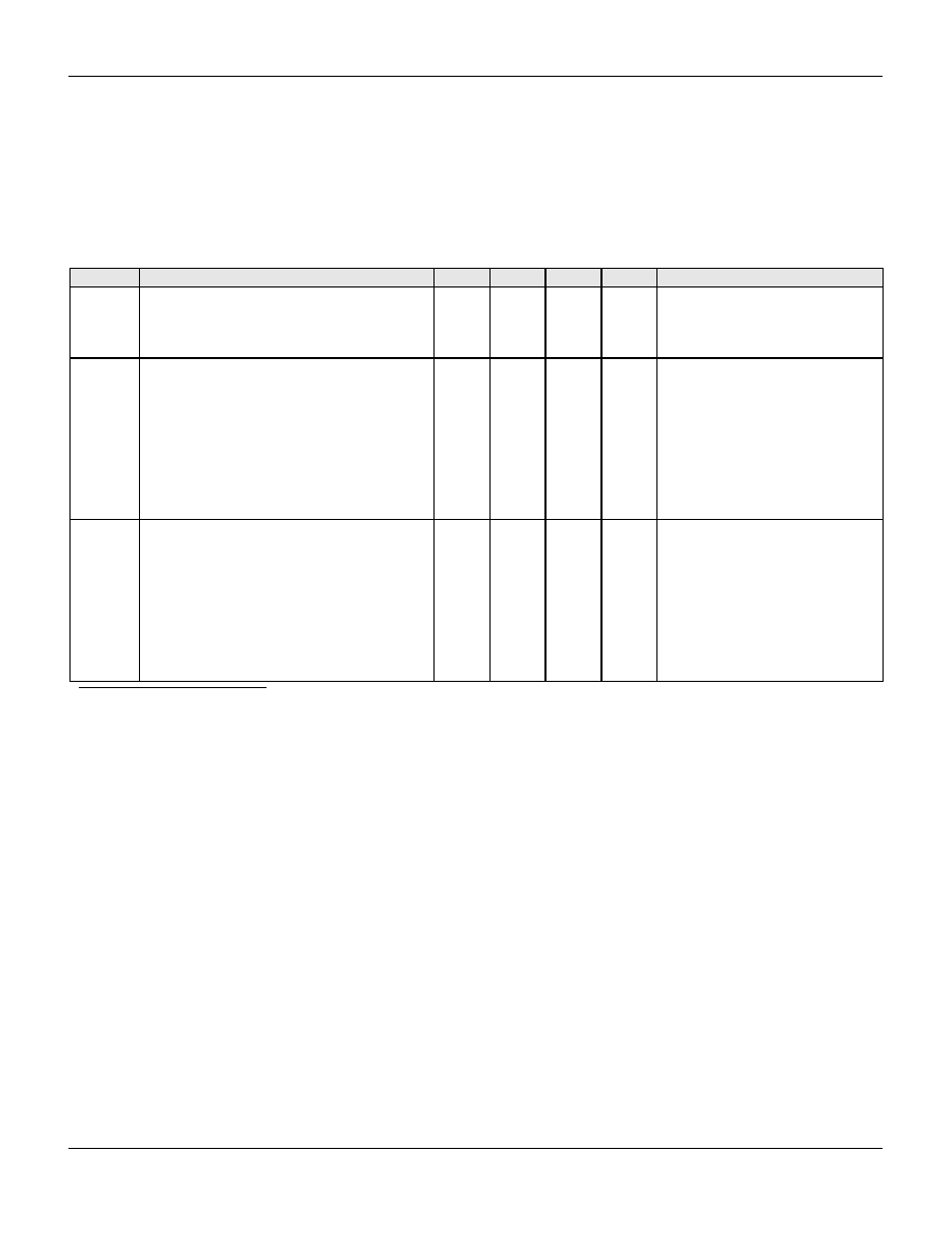
September 8, 2004
Document No. 38-12028 Rev. *B
27
CY8C24x23A Final Data Sheet
3. Electrical Specifications
3.3.8
DC POR, SMP, and LVD Specifications
The following table lists guaranteed maximum and minimum specifications for the voltage and temperature ranges: 4.75V to 5.25V
and -40
°
C
T
A
85
°
C, 3.0V to 3.6V and -40
°
C
T
A
85
°
C, or 2.4V to 3.0V and -40
°
C
T
A
85
°
C, respectively. Typical parameters
apply to 5V, 3.3V, and 2.7V at 25
°
C and are for design guidance only.
Note The bits PORLEV and VM in the table below refer to bits in the VLT_CR register. See the PSoC Mixed Signal Array Technical
Reference Manual for more information on the VLT_CR register.
Table 3-18. DC POR and LVD Specifications
Symbol
Description
Min
Typ
Max
Units
Notes
V
PPOR0
V
PPOR1
V
PPOR2
Vdd Value for PPOR Trip
PORLEV[1:0] = 00b
PORLEV[1:0] = 01b
PORLEV[1:0] = 10b
2.36
2.82
4.55
2.40
2.95
4.70
V
V
V
Vdd must be greater than or equal to 2.5V
during startup, reset from the XRES pin, or
reset from Watchdog.
V
LVD0
V
LVD1
V
LVD2
V
LVD3
V
LVD4
V
LVD5
V
LVD6
V
LVD7
Vdd Value for LVD Trip
VM[2:0] = 000b
VM[2:0] = 001b
VM[2:0] = 010b
VM[2:0] = 011b
VM[2:0] = 100b
VM[2:0] = 101b
VM[2:0] = 110b
VM[2:0] = 111b
2.40
2.85
2.95
3.06
4.37
4.50
4.62
4.71
2.45
0
2.92
0
3.02
3.13
4.48
4.64
4.73
4.81
2.51
a
2.99
b
3.09
3.20
4.55
4.75
4.83
4.95
a. Always greater than 50 mV above V
PPOR
(PORLEV=00) for falling supply.
b. Always greater than 50 mV above V
PPOR
(PORLEV=01) for falling supply.
V
0
V
0
V
0
V
0
V
0
V
V
V
V
PUMP0
V
PUMP1
V
PUMP2
V
PUMP3
V
PUMP4
V
PUMP5
V
PUMP6
V
PUMP7
Vdd Value for SMP Trip
VM[2:0] = 000b
VM[2:0] = 001b
VM[2:0] = 010b
VM[2:0] = 011b
VM[2:0] = 100b
VM[2:0] = 101b
VM[2:0] = 110b
VM[2:0] = 111b
2.50
0
2.96
3.03
3.18
4.54
4.62
4.71
4.89
2.55
0
3.02
3.10
3.25
0
4.64
4.73
4.82
5.00
2.62
c
3.09
3.16
3.32
d
4.74
4.83
4.92
5.12
c. Always greater than 50 mV above
V
LVD0
.
d. Always greater than 50 mV above
V
LVD3
.
V
V
0
V
0
V
0
V
0
V
V
V
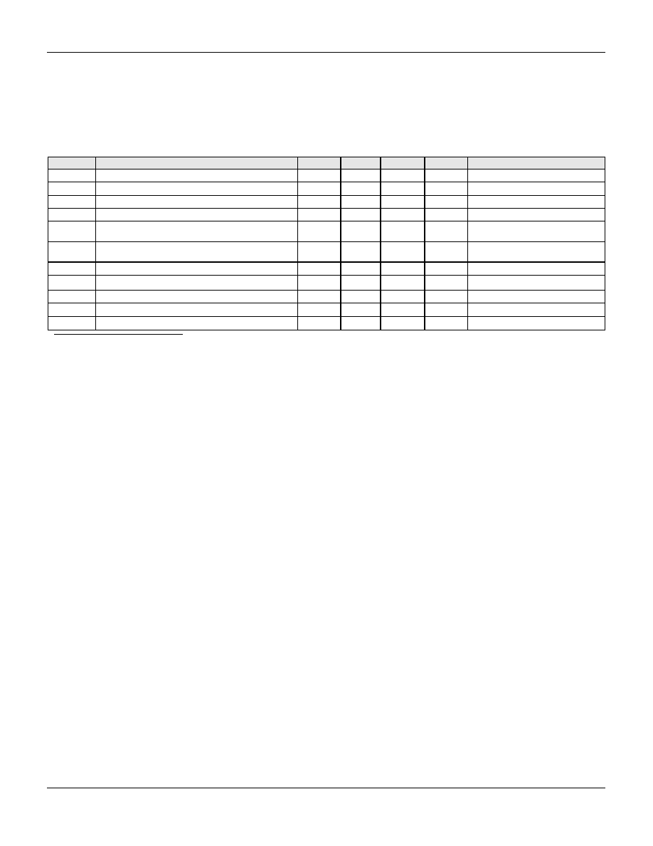
September 8, 2004
Document No. 38-12028 Rev. *B
28
CY8C24x23A Final Data Sheet
3. Electrical Specifications
3.3.9
DC Programming Specifications
The following table lists guaranteed maximum and minimum specifications for the voltage and temperature ranges: 4.75V to 5.25V
and -40
°
C
T
A
85
°
C, 3.0V to 3.6V and -40
°
C
T
A
85
°
C, or 2.4V to 3.0V and -40
°
C
T
A
85
°
C, respectively. Typical parameters
apply to 5V, 3.3V, and 2.7V at 25
°
C and are for design guidance only.
Table 3-19. DC Programming Specifications
Symbol
Description
Min
Typ
Max
Units
Notes
Vdd
IWRITE
Supply Voltage for Flash Write Operations
2.70
V
I
DDP
Supply Current During Programming or Verify
5
25
mA
V
ILP
Input Low Voltage During Programming or Verify
0.8
V
V
IHP
Input High Voltage During Programming or Verify
2.1
V
I
ILP
Input Current when Applying Vilp to P1[0] or P1[1] During
Programming or Verify
0.2
mA
Driving internal pull-down resistor.
I
IHP
Input Current when Applying Vihp to P1[0] or P1[1] During
Programming or Verify
1.5
mA
Driving internal pull-down resistor.
V
OLV
Output Low Voltage During Programming or Verify
Vss + 0.75
V
V
OHV
Output High Voltage During Programming or Verify
Vdd
- 1.0
Vdd
V
Flash
ENPB
Flash Endurance (per block)
50,000
Erase/write cycles per block.
Flash
ENT
Flash Endurance (total)
a
a. A maximum of 36 x 50,000 block endurance cycles is allowed. This may be balanced between operations on 36x1 blocks of 50,000 maximum cycles each, 36x2 blocks of
25,000 maximum cycles each, or 36x4 blocks of 12,500 maximum cycles each (to limit the total number of cycles to 36x50,000 and that no single block ever sees more than
50,000 cycles).
For the full industrial range, the user must employ a temperature sensor user module (FlashTemp) and feed the result to the temperature argument before writing. Refer to
the Flash APIs Application Note AN2015 at http://www.cypress.com under Application Notes for more information.
1,800,000
Erase/write cycles.
Flash
DR
Flash Data Retention
10
Years
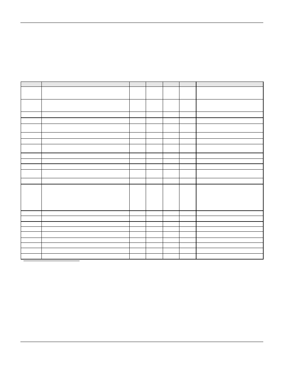
September 8, 2004
Document No. 38-12028 Rev. *B
29
CY8C24x23A Final Data Sheet
3. Electrical Specifications
3.4
AC Electrical Characteristics
3.4.1
AC Chip-Level Specifications
The following tables list guaranteed maximum and minimum specifications for the voltage and temperature ranges: 4.75V to 5.25V
and -40
°
C
T
A
85
°
C, 3.0V to 3.6V and -40
°
C
T
A
85
°
C, or 2.4V to 3.0V and -40
°
C
T
A
85
°
C, respectively. Typical parameters
apply to 5V, 3.3V, and 2.7V at 25
°
C and are for design guidance only.
Table 3-20. 5V and 3.3V AC Chip-Level Specifications
Symbol
Description
Min
Typ
Max
Units
Notes
F
IMO24
Internal Main Oscillator Frequency for 24 MHz
23.4
24
24.6
a,b,c
MHz
Trimmed for 5V or 3.3V operation using fac-
tory trim values. See Figure 3-1b on
page 15
. SLIMO Mode = 0.
F
IMO6
Internal Main Oscillator Frequency for 6 MHz
5.75
6
6.35
a,b,c
MHz
Trimmed for 5V or 3.3V operation using fac-
tory trim values. See Figure 3-1b on
page 15
. SLIMO Mode = 1.
F
CPU1
CPU Frequency (5V Nominal)
0.93
24
24.6
a,b
a. 4.75V < Vdd < 5.25V.
b. Accuracy derived from Internal Main Oscillator with appropriate trim for Vdd range.
MHz
F
CPU2
CPU Frequency (3.3V Nominal)
0.93
12
12.3
b,c
c. 3.0V < Vdd < 3.6V. See Application Note AN2012 "Adjusting PSoC Microcontroller Trims for Dual Voltage-Range Operation" for information on trimming for operation at 3.3V.
MHz
F
48M
Digital PSoC Block Frequency
0
48
49.2
a,b,d
d. See the individual user module data sheets for information on maximum frequencies for user modules.
MHz
Refer to the AC Digital Block Specifications
below.
F
24M
Digital PSoC Block Frequency
0
24
24.6
b, d
MHz
F
32K1
Internal Low Speed Oscillator Frequency
15
32
64
kHz
F
32K2
External Crystal Oscillator
32.768
kHz
Accuracy is capacitor and crystal dependent.
50% duty cycle.
F
PLL
PLL Frequency
23.986
MHz
Is a multiple (x732) of crystal frequency.
Jitter24M2
24 MHz Period Jitter (PLL)
600
ps
T
PLLSLEW
PLL Lock Time
0.5
10
ms
T
PLLSLEWS-
LOW
PLL Lock Time for Low Gain Setting
0.5
50
ms
T
OS
External Crystal Oscillator Startup to 1%
1700
2620
ms
T
OSACC
External Crystal Oscillator Startup to 100 ppm
2800
3800
ms
The crystal oscillator frequency is within 100
ppm of its final value by the end of the T
osacc
period. Correct operation assumes a prop-
erly loaded 1 uW maximum drive level
32.768 kHz crystal. 3.0V
Vdd
5.5V, -40
o
C
T
A
85
o
C.
Jitter32k
32 kHz Period Jitter
100
ns
T
XRST
External Reset Pulse Width
10
µ
s
DC24M
24 MHz Duty Cycle
40
50
60
%
Step24M
24 MHz Trim Step Size
50
kHz
Fout48M
48 MHz Output Frequency
46.8
48.0
49.2
a,c
MHz
Trimmed. Utilizing factory trim values.
Jitter24M1P
24 MHz Period Jitter (IMO) Peak-to-Peak
300
ps
Jitter24M1R
24 MHz Period Jitter (IMO) Root Mean Squared
600
ps
F
MAX
Maximum frequency of signal on row input or row output.
12.3
MHz
T
RAMP
Supply Ramp Time
0
µ
s
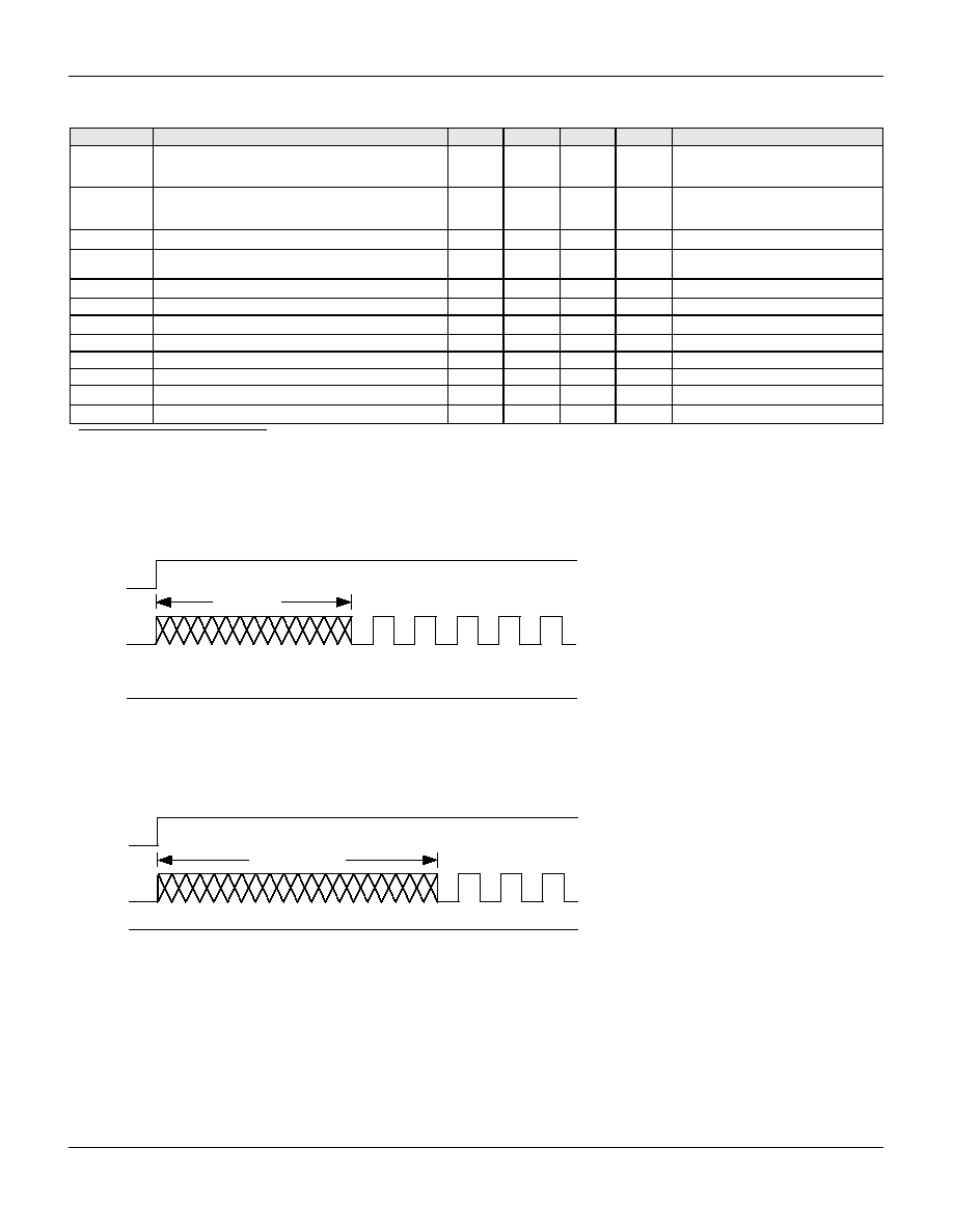
September 8, 2004
Document No. 38-12028 Rev. *B
30
CY8C24x23A Final Data Sheet
3. Electrical Specifications
Figure 3-3. PLL Lock Timing Diagram
Figure 3-4. PLL Lock for Low Gain Setting Timing Diagram
Table 3-21. 2.7V AC Chip-Level Specifications
Symbol
Description
Min
Typ
Max
Units
Notes
F
IMO12
Internal Main Oscillator Frequency for 12 MHz
11.5
12
12.7
a,b,c
MHz
Trimmed for 2.7V operation using factory
trim values. See Figure 3-1b on
page 15
.
SLIMO Mode = 1.
F
IMO6
Internal Main Oscillator Frequency for 6 MHz
5.75
6
6.35
a,b,c
MHz
Trimmed for 2.7V operation using factory
trim values. See Figure 3-1b on
page 15
.
SLIMO Mode = 1.
F
CPU1
CPU Frequency (2.7V Nominal)
0
0.93
0
3
0
3.15
a,b
MHz
0
F
BLK27
Digital PSoC Block Frequency (2.7V Nominal)
0
12
12.7
a,b,c
MHz
0
Refer to the AC Digital Block Specifica-
tions below.
F
32K1
Internal Low Speed Oscillator Frequency
8
32
96
kHz
Jitter32k
32 kHz Period Jitter
150
ns
T
XRST
External Reset Pulse Width
10
µ
s
DC12M
12 MHz Duty Cycle
40
50
60
%
Jitter12M1P
12 MHz Period Jitter (IMO) Peak-to-Peak
340
ps
Jitter12M1R
12 MHz Period Jitter (IMO) Root Mean Squared
600
ps
F
MAX
Maximum frequency of signal on row input or row output.
12.7
MHz
T
RAMP
Supply Ramp Time
0
µ
s
a. 2.4V < Vdd < 3.0V.
b. Accuracy derived from Internal Main Oscillator with appropriate trim for Vdd range.
c. See Application Note AN2012 "Adjusting PSoC Microcontroller Trims for Dual Voltage-Range Operation" for information on maximum frequency for User Modules.
24 MHz
F
PLL
PLL
Enable
T
PLLSLEW
PLL
Gain
0
24 MHz
F
PLL
PLL
Enable
T
PLLSLEWLOW
PLL
Gain
1
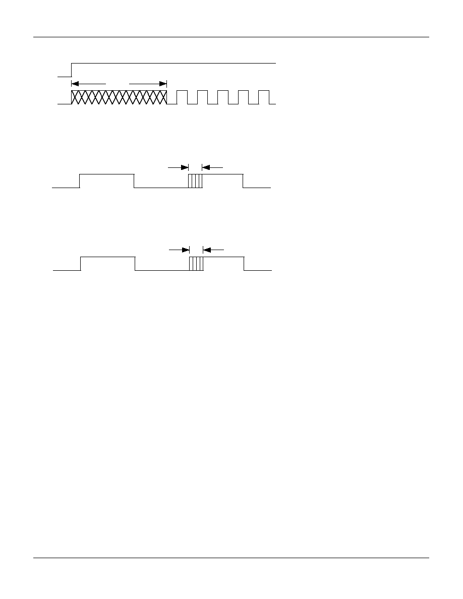
September 8, 2004
Document No. 38-12028 Rev. *B
31
CY8C24x23A Final Data Sheet
3. Electrical Specifications
Figure 3-5. External Crystal Oscillator Startup Timing Diagram
Figure 3-6. 24 MHz Period Jitter (IMO) Timing Diagram
Figure 3-7. 32 kHz Period Jitter (ECO) Timing Diagram
32 kHz
F
32K2
32K
Select
T
OS
Jitter24M1
F
24M
Jitter32k
F
32K2
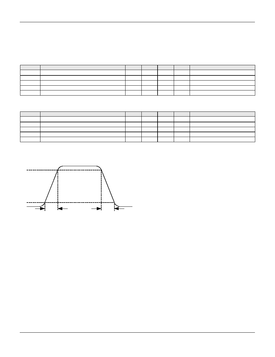
September 8, 2004
Document No. 38-12028 Rev. *B
32
CY8C24x23A Final Data Sheet
3. Electrical Specifications
3.4.2
AC General Purpose IO Specifications
The following tables list guaranteed maximum and minimum specifications for the voltage and temperature ranges: 4.75V to 5.25V
and -40
°
C
T
A
85
°
C, 3.0V to 3.6V and -40
°
C
T
A
85
°
C, or 2.4V to 3.0V and -40
°
C
T
A
85
°
C, respectively. Typical parameters
apply to 5V, 3.3V, and 2.7V at 25
°
C and are for design guidance only.
Figure 3-8. GPIO Timing Diagram
Table 3-22. 5V and 3.3V AC GPIO Specifications
Symbol
Description
Min
Typ
Max
Units
Notes
F
GPIO
GPIO Operating Frequency
0
12
MHz
Normal Strong Mode
TRiseF
Rise Time, Normal Strong Mode, Cload = 50 pF
3
18
ns
Vdd = 4.5 to 5.25V, 10% - 90%
TFallF
Fall Time, Normal Strong Mode, Cload = 50 pF
2
18
ns
Vdd = 4.5 to 5.25V, 10% - 90%
TRiseS
Rise Time, Slow Strong Mode, Cload = 50 pF
10
27
ns
Vdd = 3 to 5.25V, 10% - 90%
TFallS
Fall Time, Slow Strong Mode, Cload = 50 pF
10
22
ns
Vdd = 3 to 5.25V, 10% - 90%
Table 3-23. 2.7V AC GPIO Specifications
Symbol
Description
Min
Typ
Max
Units
Notes
F
GPIO
GPIO Operating Frequency
0
3
MHz
Normal Strong Mode
TRiseF
Rise Time, Normal Strong Mode, Cload = 50 pF
6
50
ns
Vdd = 2.4 to 3.0V, 10% - 90%
TFallF
Fall Time, Normal Strong Mode, Cload = 50 pF
6
50
ns
Vdd = 2.4 to 3.0V, 10% - 90%
TRiseS
Rise Time, Slow Strong Mode, Cload = 50 pF
18
40
120
ns
Vdd = 2.4 to 3.0V, 10% - 90%
TFallS
Fall Time, Slow Strong Mode, Cload = 50 pF
18
40
120
ns
Vdd = 2.4 to 3.0V, 10% - 90%
TFallF
TFallS
TRiseF
TRiseS
90%
10%
GPIO
Pin
Output
Voltage
September 8, 2004
Document No. 38-12028 Rev. *B
33
CY8C24x23A Final Data Sheet
3. Electrical Specifications
3.4.3
AC Operational Amplifier Specifications
The following tables list guaranteed maximum and minimum specifications for the voltage and temperature ranges: 4.75V to 5.25V
and -40
°
C
T
A
85
°
C, 3.0V to 3.6V and -40
°
C
T
A
85
°
C, or 2.4V to 3.0V and -40
°
C
T
A
85
°
C, respectively. Typical parameters
apply to 5V, 3.3V, and 2.7V at 25
°
C and are for design guidance only.
Settling times, slew rates, and gain bandwidth are based on the Analog Continuous Time PSoC block.
Power = High and Opamp Bias = High is not supported at 3.3V and 2.7V.
Table 3-24. 5V AC Operational Amplifier Specifications
Symbol
Description
Min
Typ
Max
Units
Notes
T
ROA
Rising Settling Time from 80% of
V to 0.1% of
V (10 pF
load, Unity Gain)
Power = Low, Opamp Bias = Low
Power = Medium, Opamp Bias = High
Power = High, Opamp Bias = High
3.9
0.72
0.62
µ
s
µ
s
µ
s
T
SOA
Falling Settling Time from 20% of
V to 0.1% of
V (10 pF
load, Unity Gain)
Power = Low, Opamp Bias = Low
Power = Medium, Opamp Bias = High
Power = High, Opamp Bias = High
5.9
0.92
0.72
µ
s
µ
s
µ
s
SR
ROA
Rising Slew Rate (20% to 80%)(10 pF load, Unity Gain)
Power = Low, Opamp Bias = Low
Power = Medium, Opamp Bias = High
Power = High, Opamp Bias = High
0.15
1.7
6.5
V/
µ
s
V/
µ
s
V/
µ
s
SR
FOA
Falling Slew Rate (20% to 80%)(10 pF load, Unity Gain)
Power = Low, Opamp Bias = Low
Power = Medium, Opamp Bias = High
Power = High, Opamp Bias = High
0.01
0.5
4.0
V/
µ
s
V/
µ
s
V/
µ
s
BW
OA
Gain Bandwidth Product
Power = Low, Opamp Bias = Low
Power = Medium, Opamp Bias = High
Power = High, Opamp Bias = High
0.75
3.1
5.4
MHz
MHz
MHz
E
NOA
Noise at 1 kHz (Power = Medium, Opamp Bias = High)
100
nV/rt-Hz
Table 3-25. 3.3V AC Operational Amplifier Specifications
Symbol
Description
Min
Typ
Max
Units
Notes
T
ROA
Rising Settling Time from 80% of
V to 0.1% of
V (10 pF
load, Unity Gain)
Power = Low, Opamp Bias = Low
Power = Medium, Opamp Bias = High
3.92
0.72
µ
s
µ
s
T
SOA
Falling Settling Time from 20% of
V to 0.1% of
V (10 pF
load, Unity Gain)
Power = Low, Opamp Bias = Low
Power = Medium, Opamp Bias = High
5.41
0.72
µ
s
µ
s
SR
ROA
Rising Slew Rate (20% to 80%)(10 pF load, Unity Gain)
Power = Low, Opamp Bias = Low
Power = Medium, Opamp Bias = High
0.31
2.7
V/
µ
s
V/
µ
s
SR
FOA
Falling Slew Rate (20% to 80%)(10 pF load, Unity Gain)
Power = Low, Opamp Bias = Low
Power = Medium, Opamp Bias = High
0.24
1.8
V/
µ
s
V/
µ
s
BW
OA
Gain Bandwidth Product
Power = Low, Opamp Bias = Low
Power = Medium, Opamp Bias = High
0.67
2.8
MHz
MHz
E
NOA
Noise at 1 kHz (Power = Medium, Opamp Bias = High)
100
nV/rt-Hz
September 8, 2004
Document No. 38-12028 Rev. *B
34
CY8C24x23A Final Data Sheet
3. Electrical Specifications
3.4.4
AC Digital Block Specifications
The following tables list guaranteed maximum and minimum specifications for the voltage and temperature ranges: 4.75V to 5.25V
and -40
°
C
T
A
85
°
C, 3.0V to 3.6V and -40
°
C
T
A
85
°
C, or 2.4V to 3.0V and -40
°
C
T
A
85
°
C, respectively. Typical parameters
apply to 5V, 3.3V, and 2.7V at 25
°
C and are for design guidance only.
Table 3-26. 2.7V AC Operational Amplifier Specifications
Symbol
Description
Min
Typ
Max
Units
Notes
T
ROA
Rising Settling Time from 80% of
V to 0.1% of
V (10 pF
load, Unity Gain)
Power = Low, Opamp Bias = Low
Power = Medium, Opamp Bias = High
3.92
0.72
µ
s
µ
s
T
SOA
Falling Settling Time from 20% of
V to 0.1% of
V (10 pF
load, Unity Gain)
Power = Low, Opamp Bias = Low
Power = Medium, Opamp Bias = High
5.41
0.72
µ
s
µ
s
SR
ROA
Rising Slew Rate (20% to 80%)(10 pF load, Unity Gain)
Power = Low, Opamp Bias = Low
Power = Medium, Opamp Bias = High
0.31
2.7
V/
µ
s
V/
µ
s
SR
FOA
Falling Slew Rate (20% to 80%)(10 pF load, Unity Gain)
Power = Low, Opamp Bias = Low
Power = Medium, Opamp Bias = High
0.24
1.8
V/
µ
s
V/
µ
s
BW
OA
Gain Bandwidth Product
Power = Low, Opamp Bias = Low
Power = Medium, Opamp Bias = High
0.67
2.8
MHz
MHz
E
NOA
Noise at 1 kHz (Power = Medium, Opamp Bias = High)
100
nV/rt-Hz
Table 3-27. 5V and 3.3V AC Digital Block Specifications
Function
Description
Min
Typ
Max
Units
Notes
Timer
Capture Pulse Width
50
a
a. 50 ns minimum input pulse width is based on the input synchronizers running at 24 MHz (42 ns nominal period).
ns
Maximum Frequency, No Capture
49.2
MHz
4.75V < Vdd < 5.25V.
Maximum Frequency, With Capture
24.6
MHz
Counter
Enable Pulse Width
50
a
ns
Maximum Frequency, No Enable Input
49.2
MHz
4.75V < Vdd < 5.25V.
Maximum Frequency, Enable Input
24.6
MHz
Dead Band
Kill Pulse Width:
Asynchronous Restart Mode
20
ns
Synchronous Restart Mode
50
a
ns
Disable Mode
50
a
ns
Maximum Frequency
49.2
MHz
4.75V < Vdd < 5.25V.
CRCPRS
(PRS Mode)
Maximum Input Clock Frequency
49.2
MHz
4.75V < Vdd < 5.25V.
CRCPRS
(CRC Mode)
Maximum Input Clock Frequency
24.6
MHz
SPIM
Maximum Input Clock Frequency
8.2
MHz
Maximum data rate at 4.1 MHz due to 2 x over
clocking.
SPIS
Maximum Input Clock Frequency
4.1
ns
Width of SS_ Negated Between Transmissions
50
a
ns
Transmitter
Maximum Input Clock Frequency
24.6
MHz
Maximum data rate
at 3.08 MHz due to 8 x over
clocking.
Receiver
Maximum Input Clock Frequency
24.6
MHz
Maximum data rate
at 3.08 MHz due to 8 x over
clocking.
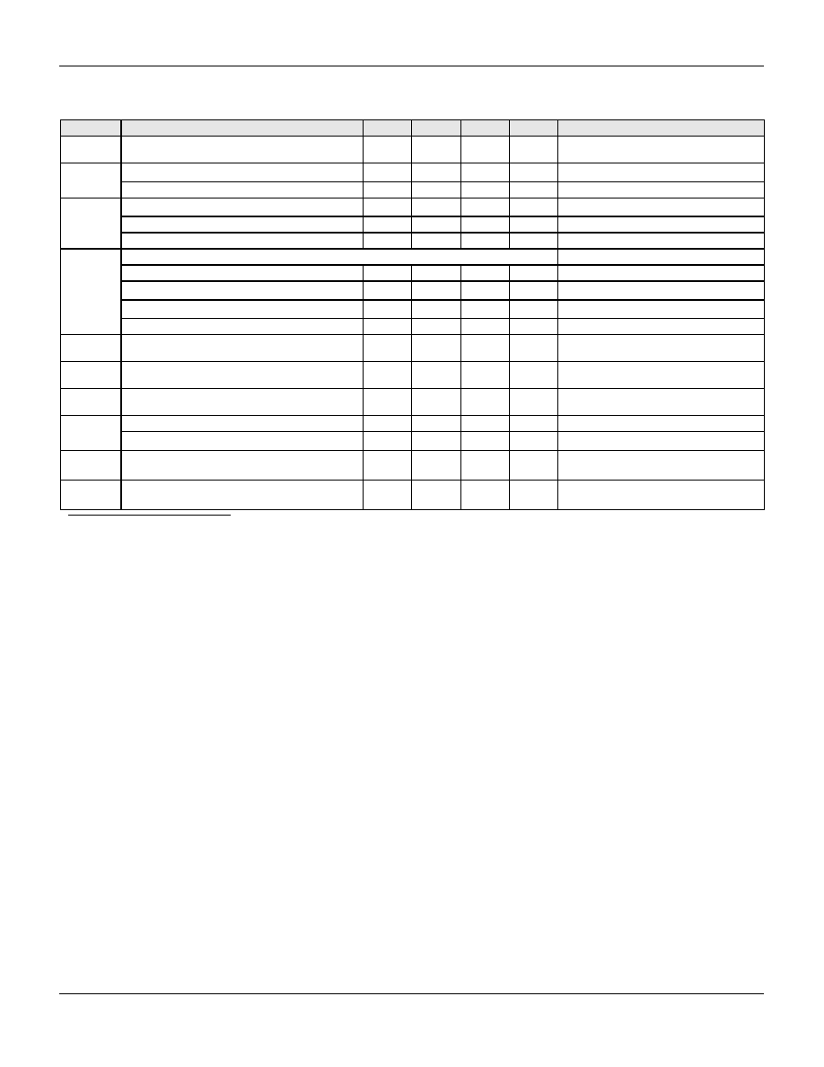
September 8, 2004
Document No. 38-12028 Rev. *B
35
CY8C24x23A Final Data Sheet
3. Electrical Specifications
Table 3-28. 2.7V AC Digital Block Specifications
Function
Description
Min
Typ
Max
Units
Notes
All
Functions
Maximum Block Clocking Frequency
12.7
MHz
2.4V < Vdd < 3.0V.
Timer
Capture Pulse Width
100
a
a. 50 ns minimum input pulse width is based on the input synchronizers running at 12 MHz (84 ns nominal period).
0
0
ns
Maximum Frequency, With or Without Capture
12.7
MHz
Counter
Enable Pulse Width
100
a
0
0
ns
Maximum Frequency, No Enable Input
12.7
MHz
Maximum Frequency, Enable Input
12.7
MHz
Dead Band
Kill Pulse Width:
Asynchronous Restart Mode
20
ns
Synchronous Restart Mode
100
a
0
0
ns
Disable Mode
0
100
a
0
0
ns
Maximum Frequency
12.7
MHz
CRCPRS
(PRS Mode)
Maximum Input Clock Frequency
12.7
MHz
CRCPRS
(CRC Mode)
Maximum Input Clock Frequency
12.7
MHz
SPIM
Maximum Input Clock Frequency
6.35
MHz
Maximum data rate at 3.17 MHz due to 2 x over
clocking.
SPIS
Maximum Input Clock Frequency
4.23
ns
Width of SS_ Negated Between Transmissions
100
a
0
0
ns
Transmitter
Maximum Input Clock Frequency
12.7
MHz
Maximum data rate
at 1.59 MHz due to 8 x over
clocking.
Receiver
Maximum Input Clock Frequency
12.7
MHz
Maximum data rate
at 1.59 MHz due to 8 x over
clocking.
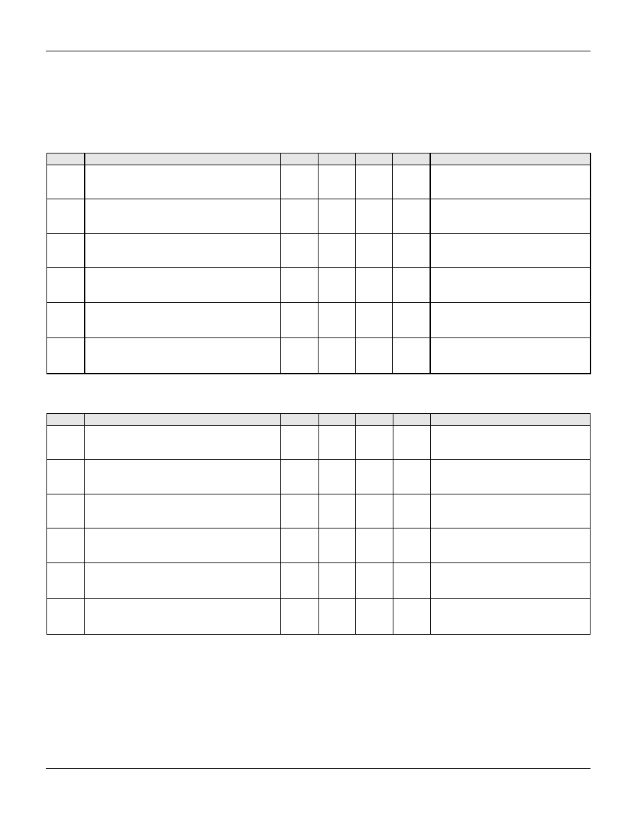
September 8, 2004
Document No. 38-12028 Rev. *B
36
CY8C24x23A Final Data Sheet
3. Electrical Specifications
3.4.5
AC Analog Output Buffer Specifications
The following tables list guaranteed maximum and minimum specifications for the voltage and temperature ranges: 4.75V to 5.25V
and -40
°
C
T
A
85
°
C, 3.0V to 3.6V and -40
°
C
T
A
85
°
C, or 2.4V to 3.0V and -40
°
C
T
A
85
°
C, respectively. Typical parameters
apply to 5V, 3.3V, and 2.7V at 25
°
C and are for design guidance only.
Table 3-29. 5V AC Analog Output Buffer Specifications
Symbol
Description
Min
Typ
Max
Units
Notes
T
ROB
Rising Settling Time to 0.1%, 1V Step, 100pF Load
Power = Low
Power = High
2.5
2.5
µ
s
µ
s
T
SOB
Falling Settling Time to 0.1%, 1V Step, 100pF Load
Power = Low
Power = High
2.2
2.2
µ
s
µ
s
SR
ROB
Rising Slew Rate (20% to 80%), 1V Step, 100pF Load
Power = Low
Power = High
0.65
0.65
V/
µ
s
V/
µ
s
SR
FOB
Falling Slew Rate (80% to 20%), 1V Step, 100pF Load
Power = Low
Power = High
0.65
0.65
V/
µ
s
V/
µ
s
BW
OB
Small Signal Bandwidth, 20mV
pp
, 3dB BW, 100pF Load
Power = Low
Power = High
0.8
0.8
MHz
MHz
BW
OB
Large Signal Bandwidth, 1V
pp
, 3dB BW, 100pF Load
Power = Low
Power = High
300
300
kHz
kHz
Table 3-30. 3.3V AC Analog Output Buffer Specifications
Symbol
Description
Min
Typ
Max
Units
Notes
T
ROB
Rising Settling Time to 0.1%, 1V Step, 100pF Load
Power = Low
Power = High
3.8
3.8
µ
s
µ
s
T
SOB
Falling Settling Time to 0.1%, 1V Step, 100pF Load
Power = Low
Power = High
2.6
2.6
µ
s
µ
s
SR
ROB
Rising Slew Rate (20% to 80%), 1V Step, 100pF Load
Power = Low
Power = High
0.5
0.5
V/
µ
s
V/
µ
s
SR
FOB
Falling Slew Rate (80% to 20%), 1V Step, 100pF Load
Power = Low
Power = High
0.5
0.5
V/
µ
s
V/
µ
s
BW
OB
Small Signal Bandwidth, 20mV
pp
, 3dB BW, 100pF Load
Power = Low
Power = High
0.7
0.7
MHz
MHz
BW
OB
Large Signal Bandwidth, 1V
pp
, 3dB BW, 100pF Load
Power = Low
Power = High
200
200
kHz
kHz
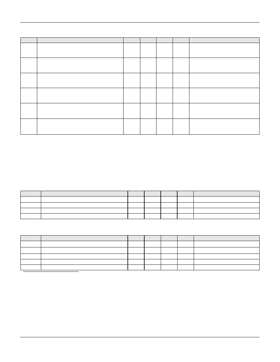
September 8, 2004
Document No. 38-12028 Rev. *B
37
CY8C24x23A Final Data Sheet
3. Electrical Specifications
3.4.6
AC External Clock Specifications
The following tables list guaranteed maximum and minimum specifications for the voltage and temperature ranges: 4.75V to 5.25V
and -40
°
C
T
A
85
°
C, 3.0V to 3.6V and -40
°
C
T
A
85
°
C, or 2.4V to 3.0V and -40
°
C
T
A
85
°
C, respectively. Typical parameters
apply to 5V, 3.3V, and 2.7V at 25
°
C and are for design guidance only.
Table 3-31. 2.7V AC Analog Output Buffer Specifications
Symbol
Description
Min
Typ
Max
Units
Notes
T
ROB
Rising Settling Time to 0.1%, 1V Step, 100pF Load
Power = Low
Power = High
4
4
µ
s
µ
s
T
SOB
Falling Settling Time to 0.1%, 1V Step, 100pF Load
Power = Low
Power = High
3
3
µ
s
µ
s
SR
ROB
Rising Slew Rate (20% to 80%), 1V Step, 100pF Load
Power = Low
Power = High
0.4
0.4
V/
µ
s
V/
µ
s
SR
FOB
Falling Slew Rate (80% to 20%), 1V Step, 100pF Load
Power = Low
Power = High
0.4
0.4
V/
µ
s
V/
µ
s
BW
OB
Small Signal Bandwidth, 20mV
pp
, 3dB BW, 100pF Load
Power = Low
Power = High
0.6
0.6
MHz
MHz
BW
OB
Large Signal Bandwidth, 1V
pp
, 3dB BW, 100pF Load
Power = Low
Power = High
180
180
kHz
kHz
Table 3-32. 5V AC External Clock Specifications
Symbol
Description
Min
Typ
Max
Units
Notes
F
OSCEXT
Frequency
0.093
24.6
MHz
High Period
20.6
5300
ns
Low Period
20.6
ns
Power Up IMO to Switch
150
µ
s
Table 3-33. 3.3V AC External Clock Specifications
Symbol
Description
Min
Typ
Max
Units
Notes
F
OSCEXT
Frequency with CPU Clock divide by 1
a
a. Maximum CPU frequency is 12 MHz at 3.3V. With the CPU clock divider set to 1, the external clock must adhere to the maximum frequency and duty cycle requirements.
0.093
12.3
MHz
F
OSCEXT
Frequency with CPU Clock divide by 2 or greater
b
b. If the frequency of the external clock is greater than 12 MHz, the CPU clock divider must be set to 2 or greater. In this case, the CPU clock divider will ensure that the fifty per-
cent duty cycle requirement is met.
0.186
24.6
MHz
High Period with CPU Clock divide by 1
41.7
5300
ns
Low Period with CPU Clock divide by 1
41.7
ns
Power Up IMO to Switch
150
µ
s
September 8, 2004
Document No. 38-12028 Rev. *B
38
CY8C24x23A Final Data Sheet
3. Electrical Specifications
3.4.7
AC Programming Specifications
The following table lists guaranteed maximum and minimum specifications for the voltage and temperature ranges: 4.75V to 5.25V
and -40
°
C
T
A
85
°
C, 3.0V to 3.6V and -40
°
C
T
A
85
°
C, or 2.4V to 3.0V and -40
°
C
T
A
85
°
C, respectively. Typical parameters
apply to 5V, 3.3V, and 2.7V at 25
°
C and are for design guidance only.
Table 3-34. 2.7V AC External Clock Specifications
Symbol
Description
Min
Typ
Max
Units
Notes
F
OSCEXT
Frequency with CPU Clock divide by 1
a
0.093
12.3
MHz
F
OSCEXT
Frequency with CPU Clock divide by 2 or greater
b
0.186
12.3
MHz
High Period with CPU Clock divide by 1
41.7
5300
ns
Low Period with CPU Clock divide by 1
41.7
ns
Power Up IMO to Switch
150
µ
s
a. Maximum CPU frequency is 12 MHz at 3.3V. With the CPU clock divider set to 1, the external clock must adhere to the maximum frequency and duty cycle requirements.
b. If the frequency of the external clock is greater than 12 MHz, the CPU clock divider must be set to 2 or greater. In this case, the CPU clock divider will ensure that the fifty per-
cent duty cycle requirement is met.
Table 3-35. AC Programming Specifications
Symbol
Description
Min
Typ
Max
Units
Notes
T
RSCLK
Rise Time of SCLK
1
20
ns
T
FSCLK
Fall Time of SCLK
1
20
ns
T
SSCLK
Data Set up Time to Falling Edge of SCLK
40
ns
T
HSCLK
Data Hold Time from Falling Edge of SCLK
40
ns
F
SCLK
Frequency of SCLK
0
8
MHz
T
ERASEB
Flash Erase Time (Block)
20
ms
T
WRITE
Flash Block Write Time
20
ms
T
DSCLK
Data Out Delay from Falling Edge of SCLK
45
ns
Vdd
>
3.6
T
DSCLK3
Data Out Delay from Falling Edge of SCLK
50
ns
3.0
Vdd
3.6
T
DSCLK2
Data Out Delay from Falling Edge of SCLK
70
ns
2.4
Vdd
3.0
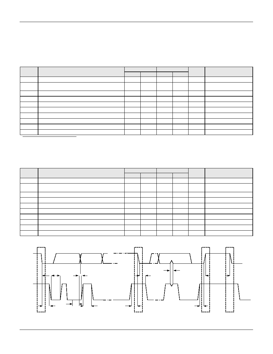
September 8, 2004
Document No. 38-12028 Rev. *B
39
CY8C24x23A Final Data Sheet
3. Electrical Specifications
3.4.8
AC I
2
C Specifications
The following tables list guaranteed maximum and minimum specifications for the voltage and temperature ranges: 4.75V to 5.25V
and -40
°
C
T
A
85
°
C, 3.0V to 3.6V and -40
°
C
T
A
85
°
C, or 2.4V to 3.0V and -40
°
C
T
A
85
°
C, respectively. Typical parameters
apply to 5V, 3.3V, and 2.7V at 25
°
C and are for design guidance only.
Figure 3-9. Definition for Timing for Fast/Standard Mode on the I
2
C Bus
Table 3-36. AC Characteristics of the I
2
C SDA and SCL Pins for Vdd > 3.0V
Symbol
Description
Standard Mode
Fast Mode
Units
Notes
Min
Max
Min
Max
F
SCLI2C
SCL Clock Frequency
0
100
0
400
kHz
T
HDSTAI2C
Hold Time (repeated) START Condition. After this period, the
first clock pulse is generated.
4.0
0.6
µ
s
T
LOWI2C
LOW Period of the SCL Clock
4.7
1.3
µ
s
T
HIGHI2C
HIGH Period of the SCL Clock
4.0
0.6
µ
s
T
SUSTAI2C
Set-up Time for a Repeated START Condition
4.7
0.6
µ
s
T
HDDATI2C
Data Hold Time
0
0
µ
s
T
SUDATI2C
Data Set-up Time
250
100
a
a. A Fast-Mode I2C-bus device can be used in a Standard-Mode I2C-bus system, but the requirement t
SU;DAT
250 ns must then be met. This will automatically be the case if
the device does not stretch the LOW period of the SCL signal. If such device does stretch the LOW period of the SCL signal, it must output the next data bit to the SDA line
t
rmax
+ t
SU;DAT
= 1000 + 250 = 1250 ns (according to the Standard-Mode I2C-bus specification) before the SCL line is released.
ns
T
SUSTOI2C
Set-up Time for STOP Condition
4.0
0.6
µ
s
T
BUFI2C
Bus Free Time Between a STOP and START Condition
4.7
1.3
µ
s
T
SPI2C
Pulse Width of spikes are suppressed by the input filter.
0
50
ns
Table 3-37. AC Characteristics of the I
2
C SDA and SCL Pins for Vdd
<
3.0V (Fast Mode Not Supported)
Symbol
Description
Standard Mode
Fast Mode
Units
Notes
Min
Max
Min
Max
F
SCLI2C
SCL Clock Frequency
0
100
kHz
T
HDSTAI2C
Hold Time (repeated) START Condition. After this period, the
first clock pulse is generated.
4.0
µ
s
T
LOWI2C
LOW Period of the SCL Clock
4.7
µ
s
T
HIGHI2C
HIGH Period of the SCL Clock
4.0
µ
s
T
SUSTAI2C
Set-up Time for a Repeated START Condition
4.7
µ
s
T
HDDATI2C
Data Hold Time
0
µ
s
T
SUDATI2C
Data Set-up Time
250
ns
T
SUSTOI2C
Set-up Time for STOP Condition
4.0
µ
s
T
BUFI2C
Bus Free Time Between a STOP and START Condition
4.7
µ
s
T
SPI2C
Pulse Width of spikes are suppressed by the input filter.
ns
SDA
SCL
S
Sr
S
P
T
BUFI2C
T
SPI2C
T
HDSTAI2C
T
SUSTOI2C
T
SUSTAI2C
T
LOWI2C
T
HIGHI2C
T
HDDATI2C
T
HDSTAI2C
T
SUDATI2C
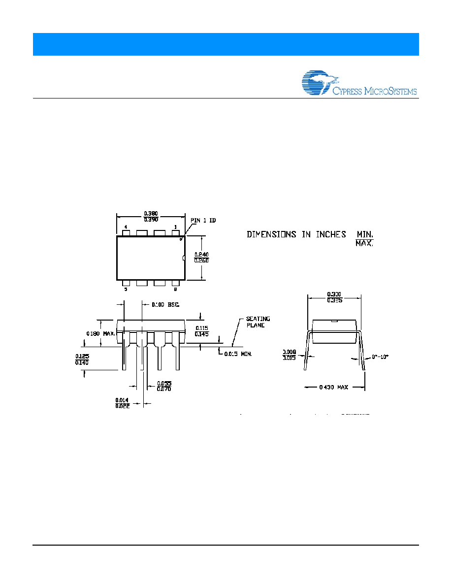
September 8, 2004
Document No. 38-12028 Rev. *B
40
4.
Packaging Information
This chapter illustrates the packaging specifications for the CY8C24x23A PSoC device, along with the thermal impedances for each
package and the typical package capacitance on crystal pins.
Important Note Emulation tools may require a larger area on the target PCB than the chip's footprint. For a detailed description of
the emulation tools' dimensions, refer to the document titled PSoC Emulator Pod Dimensions at
http://www.cypress.com/support/link.cfm?mr=poddim
.
4.1
Packaging Dimensions
Figure 4-1. 8-Lead (300-Mil) PDIP
51-85075 - *A
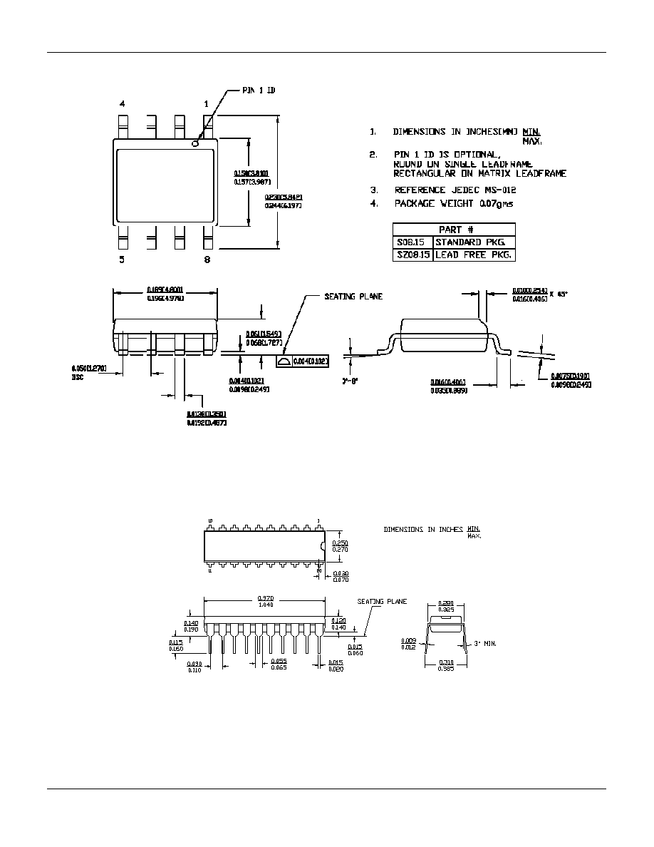
September 8, 2004
Document No. 38-12028 Rev. *B
41
CY8C24x23A Final Data Sheet
4. Packaging Information
Figure 4-2. 8-Lead (150-Mil) SOIC
Figure 4-3. 20-Lead (300-Mil) Molded DIP
51-85066 *B
51-85066 - *C
51-85011-A
20-Lead
(300-Mil)
Molded
DIPP5
51-85011 - *A
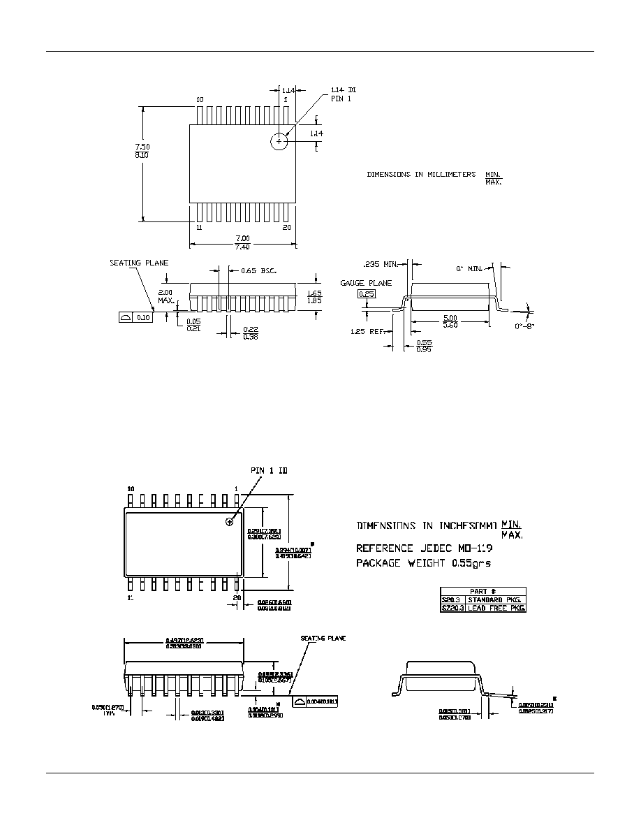
September 8, 2004
Document No. 38-12028 Rev. *B
42
CY8C24x23A Final Data Sheet
4. Packaging Information
Figure 4-4. 20-Lead (210-Mil) SSOP
Figure 4-5. 20-Lead (300-Mil) Molded SOIC
51-85077 - *C
51-85024 - *B
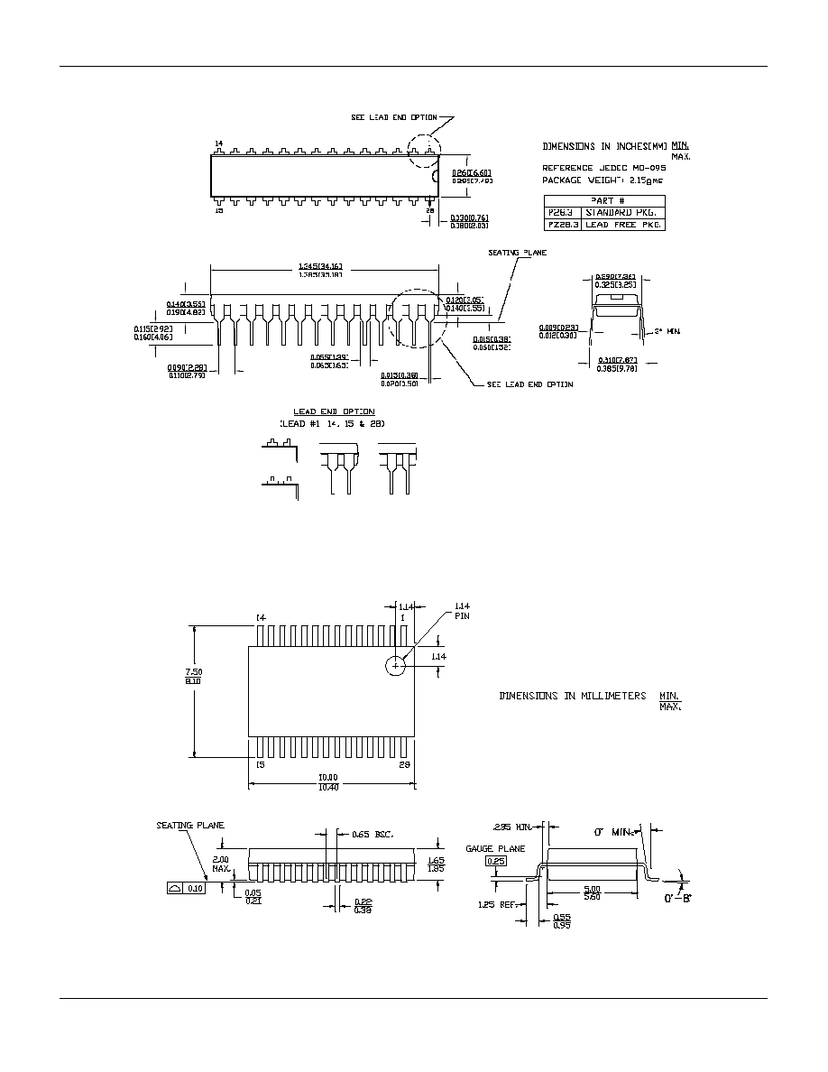
September 8, 2004
Document No. 38-12028 Rev. *B
43
CY8C24x23A Final Data Sheet
4. Packaging Information
Figure 4-6. 28-Lead (300-Mil) Molded DIP
Figure 4-7. 28-Lead (210-Mil) SSOP
51-85014 - *D
51-85079 - *C
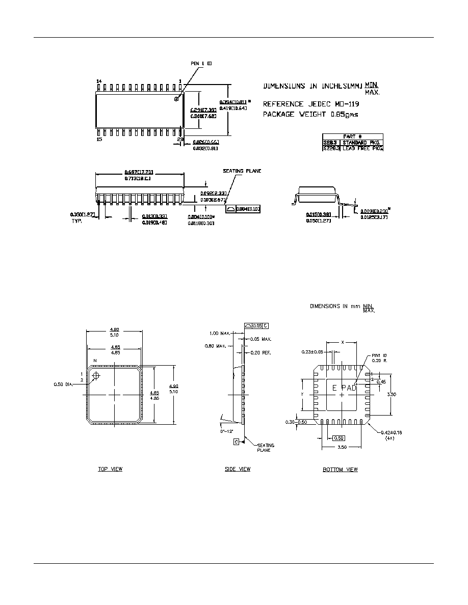
September 8, 2004
Document No. 38-12028 Rev. *B
44
CY8C24x23A Final Data Sheet
4. Packaging Information
Figure 4-8. 28-Lead (300-Mil) Molded SOIC
Figure 4-9. 32-Lead (5x5 mm) MLF
51-85026 - *C
51-85188 - **
32
X = 138 MIL
Y = 138 MIL
September 8, 2004
Document No. 38-12028 Rev. *B
45
CY8C24x23A Final Data Sheet
4. Packaging Information
4.2
Thermal Impedances
4.3
Capacitance on Crystal Pins
Table 4-1. Thermal Impedances per Package
Package
Typical
JA
*
8 PDIP
123
o
C/W
8 SOIC
185
o
C/W
20 PDIP
109
o
C/W
20 SSOP
117
o
C/W
20 SOIC
81
o
C/W
28 PDIP
69
o
C/W
28 SSOP
101
o
C/W
28 SOIC
74
o
C/W
32 MLF
22
o
C/W
* T
J
= T
A
+ POWER x
JA
Table 4-2: Typical Package Capacitance on Crystal Pins
Package
Package Capacitance
8 PDIP
2.8 pF
8 SOIC
2.0 pF
20 PDIP
3.0 pF
20 SSOP
2.6 pF
20 SOIC
2.5 pF
28 PDIP
3.5 pF
28 SSOP
2.8 pF
28 SOIC
2.7 pF
32 MLF
2.0 pF
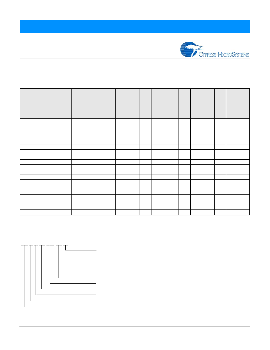
September 8, 2004
Document No. 38-12028 Rev. *B
46
5.
Ordering Information
The following table lists the CY8C24x23A PSoC device family's key package features and ordering codes.
5.1
Ordering Code Definitions
Table 5-1. CY8C24x23A PSoC Device Key Features and Ordering Information
P
ackag
e
Or
de
rin
g
Code
F
l
ash
(Kb
y
tes)
RAM
(
B
ytes)
S
wit
c
h
M
o
de
Pu
m
p
T
e
mp
eratu
r
e
Ran
g
e
Di
g
i
t
a
l
Bl
o
cks
(
R
ows
of
4
)
An
al
o
g
Bl
o
cks
(
C
o
l
um
ns
o
f
3
)
D
i
g
i
t
a
l IO
Pi
ns
A
n
a
l
og
In
pu
t
s
A
n
a
l
og
Ou
t
p
ut
s
XR
E
S
Pin
8 Pin (300 Mil) DIP
CY8C24123A-24PXI
4
256
No
-40C to +85C
4
6
6
4
2
No
8 Pin (150 Mil) SOIC
CY8C24123A-24SXI
4
256
Yes
-40C to +85C
4
6
6
4
2
No
8 Pin (150 Mil) SOIC
(Tape and Reel)
CY8C24123A-24SXIT
4
256
Yes
-40C to +85C
4
6
6
4
2
No
20 Pin (300 Mil) DIP
CY8C24223A-24PXI
4
256
Yes
-40C to +85C
4
6
16
8
2
Yes
20 Pin (210 Mil) SSOP
CY8C24223A-24PVXI
4
256
Yes
-40C to +85C
4
6
16
8
2
Yes
20 Pin (210 Mil) SSOP
(Tape and Reel)
CY8C24223A-24PVXIT
4
256
Yes
-40C to +85C
4
6
16
8
2
Yes
20 Pin (300 Mil) SOIC
CY8C24223A-24SXI
4
256
Yes
-40C to +85C
4
6
16
8
2
Yes
20 Pin (300 Mil) SOIC
(Tape and Reel)
CY8C24223A-24SXIT
4
256
Yes
-40C to +85C
4
6
16
8
2
Yes
28 Pin (300 Mil) DIP
CY8C24423A-24PXI
4
256
Yes
-40C to +85C
4
6
24
10
2
Yes
28 Pin (210 Mil) SSOP
CY8C24423A-24PVXI
4
256
Yes
-40C to +85C
4
6
24
10
2
Yes
28 Pin (210 Mil) SSOP
(Tape and Reel)
CY8C24423A-24PVXIT
4
256
Yes
-40C to +85C
4
6
24
10
2
Yes
28 Pin (300 Mil) SOIC
CY8C24423A-24SXI
4
256
Yes
-40C to +85C
4
6
24
10
2
Yes
28 Pin (300 Mil) SOIC
(Tape and Reel)
CY8C24423A-24SXIT
4
256
Yes
-40C to +85C
4
6
24
10
2
Yes
32 Pin (5x5 mm) MLF
CY8C24423A-24LFXI
4
256
Yes
-40C to +85C
4
6
24
10
2
Yes
CY 8 C 24 xxx-SPxx
Package Type:
Thermal Rating:
PX = PDIP Pb Free
C = Commercial
SX = SOIC Pb Free
I = Industrial
PVX = SSOP Pb Free
E = Extended
LFX = MLF Pb Free
AX = TQFP Pb Free
Speed: 24 MHz
Part Number
Family Code
Technology Code: C = CMOS
Marketing Code: 8 = Cypress MicroSystems
Company ID: CY = Cypress
September 8, 2004
© Cypress MicroSystems, Inc. 2004 -- Document No. 38-12028 Rev. *B
47
6.
Sales and Company Information
To obtain information about Cypress MicroSystems or PSoC sales and technical support, reference the following information or go to
the section titled
"Getting Started" on page 4
in this document.
Cypress MicroSystems
6.1
Revision History
6.2
Copyrights and Code Protection
Copyrights
© Cypress MicroSystems, Inc. 2004. All rights reserved. PSoCTM, PSoC DesignerTM, and Programmable System-on-ChipTM are trademarks of Cypress MicroSystems,
Inc. All other trademarks or registered trademarks referenced herein are property of the respective corporations.
The information contained herein is subject to change without notice. Cypress MicroSystems assumes no responsibility for the use of any circuitry other than circuitry
embodied in a Cypress MicroSystems product. Nor does it convey or imply any license under patent or other rights. Cypress MicroSystems does not authorize its products
for use as critical components in life-support systems where a malfunction or failure may reasonably be expected to result in significant injury to the user. The inclusion of
Cypress MicroSystems products in life-support systems application implies that the manufacturer assumes all risk of such use and in doing so indemnifies Cypress
MicroSystems against all charges. Cypress MicroSystems products are not warranted nor intended to be used for medical, life-support, life-saving, critical control or safety
applications, unless pursuant to an express written agreement with Cypress MicroSystems.
Flash Code Protection
Note the following details of the Flash code protection features on Cypress MicroSystems devices.
Cypress MicroSystems products meet the specifications contained in their particular Cypress MicroSystems Data Sheets. Cypress MicroSystems believes that its family of
products is one of the most secure families of its kind on the market today, regardless of how they are used. There may be methods, unknown to Cypress MicroSystems,
that can breach the code protection features. Any of these methods, to our knowledge, would be dishonest and possibly illegal. Neither Cypress MicroSystems nor any
other semiconductor manufacturer can guarantee the security of their code. Code protection does not mean that we are guaranteeing the product as "unbreakable."
Cypress MicroSystems is willing to work with the customer who is concerned about the integrity of their code. Code protection is constantly evolving. We at Cypress Micro-
Systems are committed to continuously improving the code protection features of our products.
2700 162nd Street SW
Building D
Lynnwood, WA 98037
Phone: 800.669.0557
Facsimile: 425.787.4641
Web Sites:
Company Information
http://www.cypress.com
Sales
http://www.cypress.com/aboutus/sales_locations.cfm
Technical Support
http://www.cypress.com/support/login.cfm
Table 6-1. CY8C24x23A Data Sheet Revision History
Document Title:
CY8C24123A, CY8C24223A, and CY8C24423A PSoC Mixed Signal Array Final Data Sheet
Document Number: 38-12028
Revision
ECN #
Issue Date
Origin of Change
Description of Change
**
236409
See ECN
SFV
New silicon and new document Preliminary Data Sheet.
*A
247589
See ECN
SFV
Changed the title to read "Final" data sheet. Updated Electrical Specifications chapter.
*B
261711
See ECN
HMT
Input all SFV memo changes. Updated Electrical Specifications chapter.
Distribution: External/Public
Posting: None
Document Outline