Äîêóìåíòàöèÿ è îïèñàíèÿ www.docs.chipfind.ru
PRELIMINARY
8K x 8 Magnetic Nonvolatile CMOS RAM
CY9C6264
Cypress Semiconductor Corporation
·
3901 North First Street
·
San Jose
,
CA 95134
·
408-943-2600
Document #: 38-15003 Rev. *D
Revised January 25, 2005
Features
· 100% form, fit, function compatible with 8K × 8
micropower SRAM CY6264
-- Fast Read and Write access: 70 ns
-- Voltage range: 4.5V5.5V operation
-- Low active power: 330 mW (max.)
-- Low standby power, CMOS: 495
µW (max.)
-- Easy memory expansion with CE and OE features
-- TTL-compatible inputs and outputs
-- Automatic power-down when deselected
· Replaces 8K × 8 Battery Backed (BB) SRAM, SRAM,
EEPROM, FeRAM, or Flash memory
· Data is automatically Write protected during power loss
· Write cycle endurance: >10
15
cycles
· Data Retention: >10 Years
· Shielded from external magnetic fields
· Extra 64-bytes for device identification and tracking
· Temperature ranges
-- Commercial: 0
°C to 70°C
-- Industrial: 40
°C to +85°C
· JEDEC STD 28-pin DIP (600-mil), 28-pin (300-mil) SOIC
and 28-pin TSOP-1 packages. Also available in 450-mil
wide (300-mil body width) 28-pin narrow SOIC.
Functional Description
The CY9C6264 is a high-performance CMOS nonvolatile
RAM employing an advanced magnetic RAM (MRAM)
process. An MRAM is nonvolatile memory that operates as a
fast read and write RAM. It provides data retention for more
than ten years while eliminating the reliability concerns,
functional disadvantages, and system design complexities of
battery-backed SRAM, EEPROM, Flash and FeRAM. Its fast
writes and high write cycle endurance makes it superior to
other types of nonvolatile memory.
The CY9C6264 operates very similarly to SRAM devices.
Memory read and write cycles require equal times. The MRAM
memory is nonvolatile due to its unique magnetic process.
Unlike BBSRAM, the CY9C6264 is truly a monolithic nonvol-
atile memory. It provides the same functional benefits of a fast
write without the serious disadvantages associated with
modules and batteries or hybrid memory solutions.
These capabilities make the CY9C6264 ideal for nonvolatile
memory applications requiring frequent or rapid writes in a
byte wide environment.
The CY9C6264 is offered in both commercial and industrial
temperature ranges.
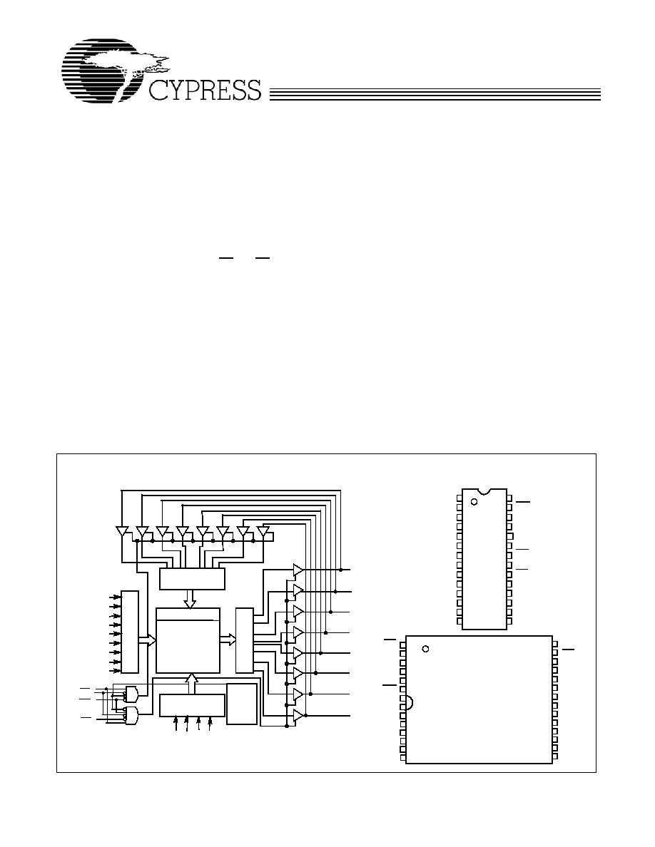
Logic Block Diagram
Pin Configurations
A
8
A
7
A
6
A
5
A
4
A
3
A
2
A
1
COLUMN
DECODER
ROW DECO
DER
SENSE AMPS
INPUTBUFFER
WE
OE
I/O
0
CE
I/O
1
I/O
2
I/O
3
1
2
3
4
5
6
7
8
9
10
11
14
15
16
20
19
18
17
21
24
23
22
Top View
SOIC/DIP
12
13
25
28
27
26
GND
A
4
A
5
A
6
A
7
A
8
A
9
A
10
A
11
WE
V
CC
A
3
A
2
A
1
I/O
7
I/O
6
I/O
5
I/O
4
A
12
NC
I/O
0
I/O
1
I/O
2
CE
1
OE
A
0
I/O
3
512 × 128
ARRAY
I/O
7
I/O
6
I/O
5
I/O
4
A
9
A
11
A
12
A
A
0
22
23
24
25
26
27
28
1
2
5
10
11
15
14
13
12
16
19
18
17
3
4
20
21
7
6
8
9
OE
A
1
A
2
A
3
WE
V
CC
A
4
A
5
A
6
A
7
A
0
CE
1
I/O
7
I/O
6
I/O
5
GND
I/O
2
I/O
1
I/O
4
I/O
0
A
12
A
11
A
10
I/O
3
TSOP I
Top View
(not to scale)
Silicon Sig.
POWER
DOWN &
WRITE
PROTECT
10
1
NC
CE
2
CE
2
A
8
A
9
CE
2
PRELIMINARY
CY9C6264
Document#: 38-15003 Rev. *D
Page 2 of 12
Overview
The CY9C6264 is a byte-wide MRAM memory. The memory
array is logically organized as 8,192 × 8 and is accessed using
an industry standard parallel asynchronous SRAM-like
interface. The CY9C6264 is inherently nonvolatile and offers
write protect during sudden power loss. Functional operation
of the MRAM is otherwise similar to SRAM-type devices.
Memory Architecture
Users access 8,192 memory locations each with eight data
bits through a parallel interface. Internally, the memory array
is organized into 8 blocks of 128 rows x 64 columns each.
The access and cycle time are the same for Read and Write
memory operations. Unlike an EEPROM or Flash, it is not
necessary to poll the device for a ready condition since writes
occur at bus speed.
Memory Operation
The CY9C6264 is designed to operate in a manner similar to
other bytewide memory products. For users familiar with
BBSRAM, the MRAM performance is superior. For users
familiar with EEPROM, Flash, and FeRAM, the obvious differ-
ences result from higher write performance of MRAM
technology and much higher write endurance.
All memory array bits are set to logic "1" at the time of
shipment.
Read Operation
A read cycle begins whenever WE (Write Enable) is inactive
(HIGH) and CE
1
(Chip Enable) and OE (Output Enable) are
active LOW while CE
2
is active HIGH. The unique address
specified by the 13 address inputs (A
0
A
12
) defines which of
the 8,192 bytes of data is to be accessed. Valid data will be
available at the eight output pins within t
AA
(access time) after
the last address input is stable, providing that CE
1
or CE
2
and
OE access times are also satisfied. If CE
1
or CE
2
and OE
access times are not satisfied, the data access must be
measured from the later-occurring signal (CE
1
, CE
2
or OE)
and the limiting parameter is either t
ACE1
for CE
1
, t
ACE2
for
CE
2
, or t
DOE
for the OE rather than address access.
Write Cycle
The CY9C6264 initiates a Write cycle whenever the WE and
CE
1
signals are active (LOW) or WE is LOW and CE
2
is HIGH,
after address inputs are stable. The later occurring falling edge
of CE
1
(rising in case of CE
2
) or WE will determine the start of
the Write cycle. The Write cycle is terminated by the earlier
rising edge of CE
1
(falling edge in case of CE
2
) or WE. All
address inputs must be kept valid throughout the Write cycle.
The OE control signal should be kept inactive (HIGH) during
Write cycles to avoid bus contention. However, if the output
drivers are enabled (CE
1
or CE
2
and OE active), WE will
disable the outputs in t
HZWE
from the WE falling edge.
Unlike other nonvolatile memory technologies, there is no
Write delay with MRAM. The entire memory operation occurs
in a single bus cycle. Therefore, any operation including Read
or Write can occur immediately following a Write. Data Polling,
a technique used with EEPROMs to determine if the Write is
complete, is unnecessary. Page Write, a technique used to
enhance EEPROM Write performance, is also unnecessary
because of inherently fast Write cycle time for MRAM. The
total write time for the entire array is 0.575 ms.
Write Inhibit and Data Retention Mode
This feature protects against the inadvertent Write. The
CY9C6264 provides full functional capability for V
CC
greater
than 4.5V and Write-protects the device below 4.0V. Data is
maintained in the absence of V
CC
. During the power-up,
normal operation can resume 20
µs after V
PFD
is reached.
Refer to page 8 for details.
Sudden Power Loss--"Brown out"
The nonvolatile RAM constantly monitors V
CC
. Should the
supply voltage decay below the operating range, the
CY9C6264 automatically write-protects itself, all inputs
become "don't care," and all outputs become high impedance.
Refer to page 8 for details.
Silicon Signature/Device ID
An extra 64 bytes of MRAM are available to the user for Device
ID. By raising A
7
to V
CC
+ 2.0V and by using address locations
00 (Hex) to 3F (Hex) on address pins A
6
, A
5
, A
4
, A
12
, A
11
, and
A
10
(MSB to LSB) respectively, the additional bytes may be
accessed in the same manner as the regular memory array
with 140ns read access time and 140ns write cycle time.
Writing the extra bytes of MRAM requires a longer address
setup to write start of 70 ns vs. the normal operating specifi-
cation of 0ns. Dropping A
7
from input high (V
CC
+ 2.0V) to <
V
CC
+ 0.5V max. returns the device to normal operation after
140-ns delay.
All User Space bits are set to logic "1" at the time of shipment.
Magnetic Shielding
CY9C6264 is protected from external magnetic fields through
the application of a "magnetic shield" that covers the entire
memory array.
Applications
Battery-backed SRAM (BBSRAM) Replacement
CY9C6264 is designed to replace (plug and play) existing
BBSRAM while eliminating the need for battery and V
CC
monitor IC, reducing cost and board space and improving
system reliability.
The cost associated with multiple components, assemblies,
and manufacturing overhead associated with battery-backed
SRAM is eliminated by using monolithic MRAM. CY9C6264
eliminates multiple assemblies, connectors, modules, field
maintenance, and environmental issues common with BB
SRAM. MRAM is a true nonvolatile RAM with high perfor-
mance, high endurance, and data retention.
Battery-backed SRAMs are forced to monitor V
CC
in order to
switch to the backup battery. Users that are modifying existing
designs to use MRAM in place of BBSRAM, can eliminate the
V
CC
controller IC along with the battery. MRAM performs this
function on-chip.
Address (MSB to LSB)
A
6
A
5
A
4
A
12
A
11
A
10
Description
ID
00h
Manufacturer ID
34h
01h
Device ID
41h
02h3Fh
User Space
62 bytes

PRELIMINARY
CY9C6264
Document#: 38-15003 Rev. *D
Page 3 of 12
Cost
The cost of both the component and manufacturing overhead
of battery-backed SRAM is high. In addition, there is a built-in
rework step required for battery attachment in case of surface
mount assembly. This can be eliminated with MRAM. In the
case of DIP battery-backed modules, the assembly
techniques are constrained to through-hole assembly and
board wash using no water.
System Reliability
Battery-backed SRAM is inherently vulnerable to shock and
vibration. In addition, a negative voltage on any pin of a
battery-backed SRAM, even a momentary undershoot, can
cause data loss. The negative voltage causes current to be
drawn directly from the battery, weakens the battery, and
reduces its capacity over time. In general, there is no way to
monitor the lost battery capacity. MRAM guarantees reliable
operation across the voltage range with inherent nonvolatility.
Space
Battery-backed SRAM in DIP modules takes up board space
height and dictates through-hole assembly. MRAM is offered
in surface mount as well as DIP packages.
Field Maintenance
Batteries must eventually be replaced, which creates an
inherent maintenance problem. Despite projections of long
life, it is difficult to know how long a battery will last, considering
all the factors that degrade them.
Environmental
Lithium batteries are a potential disposal burden and are
considered a fire hazard. MRAM eliminates all such issues
through a truly monolithic nonvolatile solution.
Users replacing battery-backed SRAMs with an integrated
Real-time Clock (RTC) in the same package may need to
move the RTC function to a different location within the
system.
EEPROM Replacement
CY9C6264 can also replace EEPROM in current applications.
CY9C6264 is pinout- and functionally-compatible to byte-wide
EEPROM, but it does not need data-bar polling, page Write,
and hardware Write protect due to its fast Write and
inadvertent Write-protect features.
Users replacing EEPROMs with MRAM can eliminate the
page mode operation and simplify to standard asynchronous
write. Additionally, data-bar polling can be eliminated, since
every byte Write is completed within same cycle. All Writes are
completed within 70 ns.
FeRAM Replacement
FeRAM requires addresses to be latched on falling edge of
CE, which adds to system overhead in managing the CE and
latching function. MRAM eliminates this overhead by offering
a simple asynchronous SRAM interface.
Users replacing FeRAM can simplify their address decoding
since you do not need to drive CE active and then inactive for
each address. This overhead is eliminated when using MRAM.
Secondly, MRAM Read is nondestructive and no precharge
cycle is required like the one used with FeRAM. This has no
apparent impact to the design, but the Read cycle time can
now see immediate improvement equal to the precharge time.
Boot Up PROM (EPROM, PROM) Function Replacement
The CY9C6264 can be accessed like an EPROM or PROM.
When CE
1
and OE are LOW and CE
2
and WE are HIGH, the
data stored at the memory location determined by the address
pins is asserted on the outputs. MRAM may be used to accom-
plish system boot up function using this condition.
PRELIMINARY
CY9C6264
Document#: 38-15003 Rev. *D
Page 4 of 12
Maximum Ratings
(Above which the useful life may be impaired. For user guide-
lines, not tested.)
Storage Temperature .................................65
°C to +150°C
Ambient Temperature with
Power Applied...............................................40
°C to +85°C
Supply Voltage to Ground Potential
(Pin 28 to Pin 14) ........................................... 0.5V to +7.0V
DC Voltage Applied to Outputs
in High-Z State
[1]
....................................0.5V to V
CC
+ 0.5V
DC Input Voltage
[1]
.................................0.5V to V
CC
+ 0.5V
except in case of super voltage pin (A7) while accessing 16
device ID and silicon signature bytes.
... -0.5V to V
CC
+ 2.5V
Output Current into Outputs (LOW)............................. 20 mA
Static Discharge Voltage.......................................... > 2001V
(per MIL-STD-883, Method 3015)
Latch-up Current..................................................... > 200 mA
Maximum Exposure to Magnetic Field
@ Device Package
[2, 3]
............................................ < 20 Oe
Operating Range
Range
Ambient Temperature
V
CC
Commercial
0°C to +70°C
5V
± 10%
Industrial
40°C to +85°C
5V
± 10%
Electrical Characteristics
Over the Operating Range
Parameter
Description
Test Conditions
CY9C62256-70
Unit
Min.
Typ.
[5]
Max.
V
OH
Output HIGH Voltage
V
CC
= Min., I
OH
=
-1.0 mA
2.4
V
V
OL
Output LOW Voltage
V
CC
= Min., I
OL
= 2.1 mA
0.4
V
V
IH
Input HIGH Voltage
2.2
V
CC
+ 0.5V
V
V
IL
Input LOW Voltage
-0.5
[1]
0.8
V
I
IX
[4]
Input Leakage Current
GND < V
I
< V
CC
-0.5
+0.5
µA
I
OZ
Output Leakage Current
GND < V
O
< V
CC
, Output Disabled
-0.5
+0.5
µA
I
CC
V
CC
Operating Supply Current V
CC
= Max., I
OUT
= 0 mA, f = f
MAX
= 1/t
RC
60
mA
I
SB1
Automatic CE Power-down
Current-- TTL Inputs
Max. V
CC
, CE
1
> V
IH
or CE
2
< V
IL
V
IN
> V
IH
or V
IN
< V
IL
, f = f
MAX
500
µA
I
SB2
Automatic CE Power-down
Current-- CMOS Inputs
Max. V
CC
,
CE
1
> V
CC
- 0.3V or CE
2
< 0.3V
V
IN
> V
CC
- 0.3V or V
IN
< 0.3V, f = 0
90
µA
Capacitance
[6]
Parameter
Description
Test Conditions
Max.
Unit
C
IN
Input Capacitance
T
A
= 25
°C, f = 1 MHz,
V
CC
= 5.0V
6
pF
C
OUT
Output Capacitance
8
pF
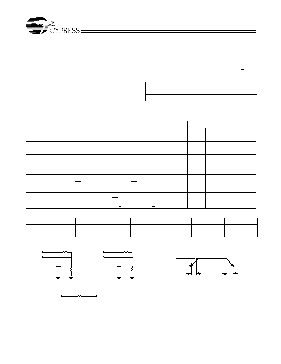
AC Test Loads and Waveforms
Notes:
1. V
IL
(min) = 2.0V for pulse duration of 20 ns.
2. Magnetic field exposure is highly dependent on the distance from the magnetic field source. The magnetic field falls of as 1/R squared, where R is the distance
from the magnetic source.
3. Exposure beyond this level may cause loss of data.
4. I
IX
during access to 16 device ID and silicon signature bytes w/ super voltage pin at V
CC
+ 2.0V will be 100
µA max., V
IL
(min.) = 2.0V for pulse duration of less
than 20 ns.
5. Typical specifications are the mean values measured over a large sample size across normal production process variations and are taken at nominal conditions
(T
A
= 25°C, V
CC
). Parameters are guaranteed by design and characterization and not 100% tested.
6. Tested initially and after any design or process changes that may affect these parameters.
3.0V
5V
OUTPUT
R1 1800
R2
990
100 pF
INCLUDING
JIG AND
SCOPE
GND
90%
10%
90%
10%
< 5 ns
< 5 ns
5V
OUTPUT
R1 1800
R2
990
5 pF
INCLUDING
JIG AND
SCOPE
(a)
(b)
OUTPUT
1.77V
Equivalent to:
THEVENIN EQUIVALENT
ALL INPUT PULSES
639
PRELIMINARY
CY9C6264
Document#: 38-15003 Rev. *D
Page 5 of 12
Switching Characteristics
Over the Operating Range
[7]
Parameter
Description
CY9C6264-70
Unit
Min.
Max.
Read Cycle
t
RC
Read Cycle Time
70
ns
t
AA
Address to Data Valid
70
ns
t
OHA
Data Hold from Address Change
5
ns
t
ACE1
CE
1
LOW to Data Valid
70
ns
t
ACE2
CE
2
HIGH to Data Valid
70
ns
t
DOE
OE LOW to Data Valid
35
ns
t
LZOE
OE LOW to Low-Z
[8]
5
ns
t
HZOE
OE HIGH to High-Z
[8, 9]
25
ns
t
LZCE1
CE
1
LOW to Low-Z
[8]
5
ns
t
LZCE2
CE
2
HIGH to Low-Z
[8]
5
ns
t
HZCE
CE
1
HIGH to High-Z
[8, 9]
CE
2
LOW to High-Z
[8, 9]
25
ns
t
PU
CE
1
LOW to Power-up
CE
2
HIGH to Power-up
0
ns
t
PD
CE
1
HIGH to Power-down
CE
2
LOW to Power-down
70
ns
Write Cycle
[10, 11]
t
WC
Write Cycle Time
70
ns
t
SCE1
CE
1
LOW to Write End
60
ns
t
SCE2
CE
2
HIGH to Write End
60
ns
t
AW
Address Set-up to Write End
60
ns
t
HA
Address Hold from Write End
0
ns
t
SA
Address Set-up to Write Start
0
ns
t
PWE
WE Pulse Width
50
ns
t
SD
Data Set-up to Write End
30
ns
t
HD
Data Hold from Write End
0
ns
t
HZWE
WE LOW to High-Z
[8, 9]
25
ns
t
LZWE
WE HIGH to Low-Z
[8]
5
ns
Notes:
7. Test conditions assume signal transition time of 5 ns or less, timing reference levels of 1.5V, input pulse levels of 0 to 3.0V, and output loading of the specified
I
OL
/I
OH
and 100-pF load capacitance.
8. At any given temperature and voltage condition, t
HZCE1
is less than t
LZCE1
, t
HZCE2
is less than t
LZCE2
, t
HZOE
is less than t
LZOE
, and t
HZWE
is less than t
LZWE
for
any given device.
9. t
HZOE
, t
HZCE
, and t
HZWE
are specified with CL = 5 pF as in (b) of AC Test Loads. Transition is measured ± 500 mV from steady-state voltage.
10. The internal Write time of the memory is defined by the overlap of CE
1
LOW or CE
2
HIGH and WE LOW. Both signals must be LOW to initiate a Write and either
signal can terminate a Write by going HIGH. The data input set-up and hold timing should be referenced to the rising edge of the signal that terminates the Write.
11. The minimum write pulse width for Write cycle #3 (WE-controlled, OE LOW) is the sum of t
HZWE
and t
SD
.
PRELIMINARY
CY9C6264
Document#: 38-15003 Rev. *D
Page 6 of 12
Switching Waveforms
Read Cycle No. 1
[12, 13]
Read Cycle No. 2
[13, 14]
Write Cycle No. 1 (WE Controlled)
[10, 15, 16]
Notes:
12. Device is continuously selected. OE = V
IL
CE
1
= V
IL
or OE = V
IL
CE
2
= V
IH
.
13. WE is HIGH for Read cycle.
14. Address valid prior to or coincident with CE
1
transition LOW or CE
2
transition to HIGH.
15. Data I/O is high impedance if OE = V
IH
.
16. If CE
1
goes HIGH Or CE
2
goes LOW simultaneously with WE HIGH, the output remains in a high-impedance state.
17. During this period, the I/Os are in output state and input signals should not be applied.
ADDRESS
DATA OUT
PREVIOUS DATA VALID
DATA VALID
t
RC
t
AA
t
OHA
50%
50%
DATA VALID
t
RC
t
ACE
t
DOE
t
LZOE
t
LZCE
t
PU
DATA OUT
HIGH IMPEDANCE
IMPEDANCE
ICC
ISB
t
HZOE
t
HZCE
t
PD
OE
CE
1
HIGH
V
CC
SUPPLY
CURRENT
CE
2
t
HD
t
SD
t
PWE
t
SA
t
HA
t
AW
t
WC
DATA I/O
ADDRESS
CE
1
WE
OE
t
HZOE
DATA IN VALID
NOTE 17
CE
2
t
SCE1
t
SCE2
PRELIMINARY
CY9C6264
Document#: 38-15003 Rev. *D
Page 7 of 12
Write Cycle No. 2 (CE
1
Or CE
2
Controlled)
[10, 15, 16]
Write Cycle No. 3 (WE Controlled, OE LOW)
[10, 15, 16, 18]
Truth Table
CE
1
CE
2
WE
OE
V
CC
Inputs/Outputs
Mode
Power
H
L
X
X
4.55.5V High-Z
Deselect/Power-down
Standby (I
SB
)
H
H
X
X
4.55.5V High-Z
Deselect/Power-down
Standby (I
SB
)
L
L
X
X
4.55.5V High-Z
Deselect/Power-down
Standby (I
SB
)
L
H
H
L
4.55.5V Data Out
Read
Active (I
CC
)
L
H
L
X
4.55.5V Data In
Write
Active (I
CC
)
L
H
H
H
4.55.5V High-Z
Deselect, Output Disabled
Active (I
CC
)
X
X
X
X
< 4.0V
Inputs = X, Outputs = High-Z Write Inhibit
Active (I
CC
)
Note:
18. If CE
1
goes HIGH and CE
2
goes LOW simultaneously with WE HIGH, the outputs remain in high-impedance state.
Switching Waveforms
(continued)
t
WC
t
AW
t
SA
t
HA
t
HD
t
SD
t
SCE1
WE
DATA I/O
ADDRESS
CE
1
DATA IN VALID
t
SCE2
CE
2
DATA I/O
ADDRESS
t
HD
t
SD
t
LZWE
t
SA
t
HA
t
AW
t
WC
CE
1
WE
t
HZWE
DATA IN VALID
NOTE 17
CE
2
t
SCE1
t
SCE2
PRELIMINARY
CY9C6264
Document#: 38-15003 Rev. *D
Page 8 of 12
Power-down/Power-up Mode AC Waveforms
Parameter
Description
Min.
Typ.
Max.
Unit
V
PFD
Power-fail Deselect Voltage
4.2
4.35
4.5
V
t
F
[19]
V
PFD
(max.) to V
PFD
(min.) V
CC
Fall Time
100
µs
t
FB
V
PFD
(min.) to V
SS
V
CC
Fall Time
50
µs
t
R
V
SS
to V
PFD
(max.) Rise Time
20
µs
t
WP
Write Protect Time On V
CC
= V
PFD
20
µs
t
REC
V
PFD
(max.) to Inputs Recognized
500
µs
V
CC
V
PFD
(max.)
V
PFD
(min.)
t
FB
t
R
t
REC
INPUTS
OUTPUTS
DON'T CARE
RECOGNIZED
VALID
VALID
HIGH-Z
t
F
RECOGNIZED
V
PFD
(typ)
t
WP
Ordering Information
Speed (ns)
Ordering Code
Package Name
Package Type
Operating Range
70
CY9C6264
-70SC
S21
28-pin (300-mil) Molded SOIC
Commercial
CY9C6264-70SI
S21
28-pin (300-mil) Molded SOIC
Industrial
CY9C6264-70SNC
SN28
28-lead (300-mil) Narrow Body SOIC
Commercial
CY9C6264-70SNI
SN28
28-lead (300-mil) Narrow Body SOIC
Industrial
CY9C6264
-70ZC
Z28
28-pin Thin Small Outline Package
Commercial
CY9C6264
-70ZI
Z28
28-pin Thin Small Outline Package
Industrial
CY9C6264
-70PC
P15
28-pin (600-mil) Molded DIP
Commercial
CY9C6264-70PI
P15
28-pin (600-mil) Molded DIP
Industrial
Note:
19. V
PFD
(max.) to V
PFD
(min.) fall time of less than t
F
may result in deselection/write protection not occurring until 20
µs after V
CC
passes V
PFD
(min.).
PRELIMINARY
CY9C6264
Document#: 38-15003 Rev. *D
Page 9 of 12
Package Diagrams
51-85017-*A
28-pin (600-Mil) Molded DIP P15
DIMENSIONS IN INCHES[MM]
MIN.
MAX.
PIN 1 ID
0.291[7.39]
0.300[7.62]
0.394[10.01]
0.419[10.64]
0.050[1.27]
TYP.
0.092[2.33]
0.105[2.67]
0.004[0.10]
0.0118[0.30]
SEATING PLANE
0.0091[0.23]
0.0125[3.17]
0.015[0.38]
0.050[1.27]
0.013[0.33]
0.019[0.48]
0.026[0.66]
0.032[0.81]
0.697[17.70]
0.713[18.11]
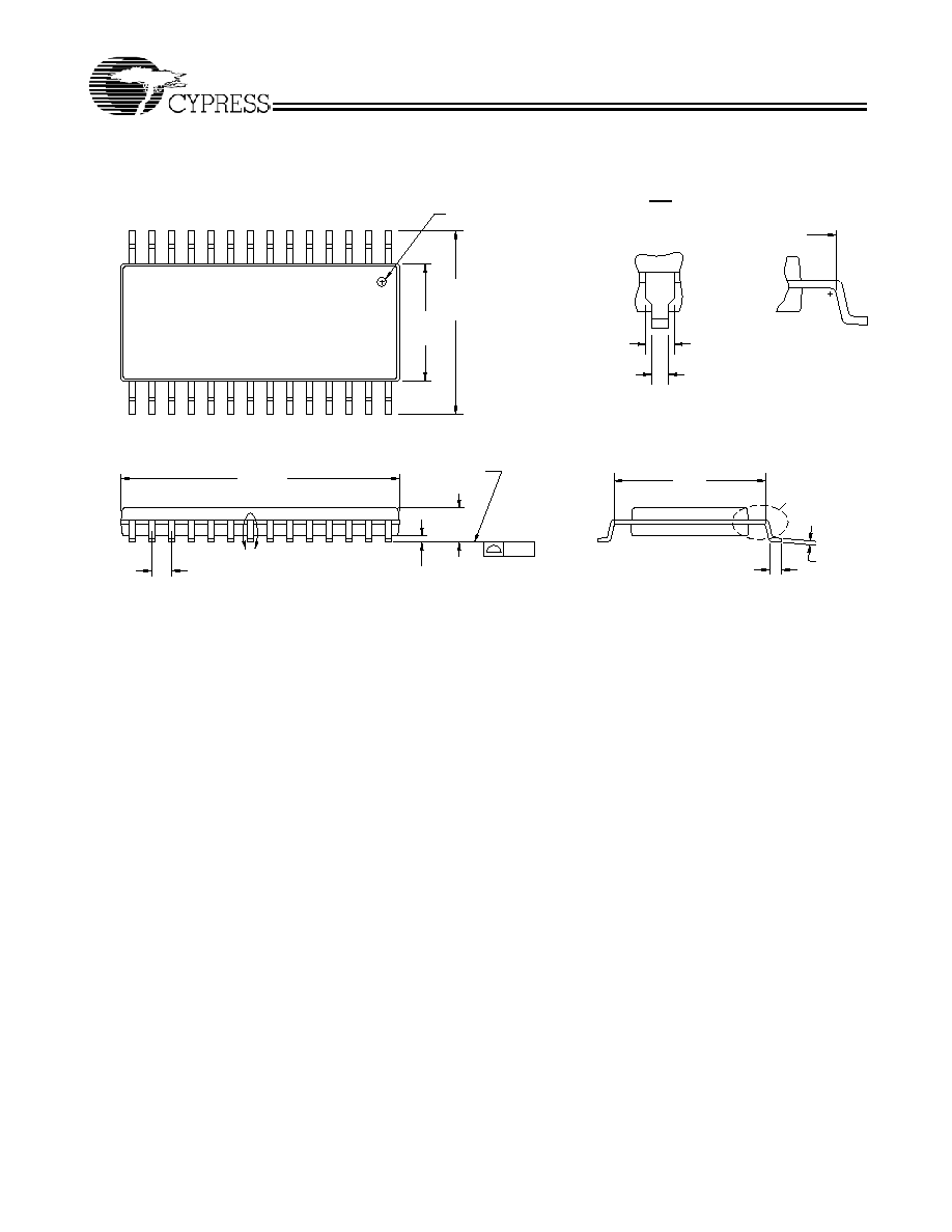
28 Lead (300 Mil) SOIC - S21
0.004[0.10]
1
14
15
28
*
*
*
REFERENCE JEDEC MO-119
PART #
S28.3 STANDARD PKG.
SZ28.3 LEAD FREE PKG.
PACKAGE WEIGHT 0.85gms
51-85026-*C
28-Lead (300-Mil) Molded SOIC S21
PRELIMINARY
CY9C6264
Document#: 38-15003 Rev. *D
Page 10 of 12
Package Diagrams
(continued)
DIMENSIONS IN INCHES
MIN.
MAX.
PIN 1 ID
0.291
0.300
0.463
0.477
0.050
TYP.
0.094
0.110
0.002
0.014
SEATING PLANE
0.008
0.012
0.702
0.710
0.020
0.042
0.004
0.014
0.020
0.020
0.015
0.032
0.026
A
OMEDATA
CSPI
DETAIL "A"
0.390
0.420
0.390
0.420
DETAIL "B"
B
450-mil Wide (300-mil Body Width) 28 Pin Narrow SOIC (SN28)
51-85092-*B
MIN.
MAX.
PRELIMINARY
CY9C6264
Document#: 38-15003 Rev. *D
Page 11 of 12
© Cypress Semiconductor Corporation, 2005. The information contained herein is subject to change without notice. Cypress Semiconductor Corporation assumes no responsibility for the use
of any circuitry other than circuitry embodied in a Cypress product. Nor does it convey or imply any license under patent or other rights. Cypress products are not warranted nor intended to be
used for medical, life support, life saving, critical control or safety applications, unless pursuant to an express written agreement with Cypress. Furthermore, Cypress does not authorize its
products for use as critical components in life-support systems where a malfunction or failure may reasonably be expected to result in significant injury to the user. The inclusion of Cypress
products in life-support systems application implies that the manufacturer assumes all risk of such use and in doing so indemnifies Cypress against all charges.
All product and company names mentioned in this document are the trademarks of their respective holders.
Package Diagrams
(continued)
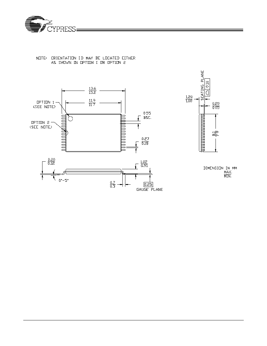
28-pin Thin Small Outline Package Type 1 (8 × 13.4 mm) Z28
51-85071-*G
PRELIMINARY
CY9C6264
Document#: 38-15003 Rev. *D
Page 12 of 12
Document History Page
Document Title: CY9C6264 8K x 8 Magnetic Nonvolatile CMOS RAM
Document Number: 38-15003
REV.
ECN NO. Issue Date
Orig. of
Change
Description of Change
**
116317
06/11/02
NBP
New Data Sheet
*A
116771
07/25/02
NBP
Add state of memory bits at the time of shipment
*B
208424
SEE ECN
NBP
Icc, Isb1, Isb2, Shielding Specification, Condition to emulate Boot PROM
functionality
*C
227582
SEE ECN
NBP
Changed Magnetic Shielding Specification
*D
309663
SEE ECN
NBP
Changed V
PFD
& t
WP
Specification, added SNC package & Silicon Signature
ID address bits.