LUPA-4000
Data Sheet
Cypress Semiconductor Corporation
3901 North First Street
San Jose, CA 95134
408-943-2600
Contact:
info@Fillfactory.com
Document #: 38-05712 Rev.**(Revision 1.2 ) Page 3 of 49
TABLE OF CONTENTS
1 PREAMBLE ..........................................................................................................5
1.1 O
VERVIEW
.........................................................................................................5
1.2 M
AIN FEATURES
................................................................................................5
1.3 P
ART
N
UMBER
...................................................................................................5
2 SPECIFICATIONS...............................................................................................6
2.1 G
ENERAL SPECIFICATIONS
.................................................................................6
2.2 E
LECTRO
-
OPTICAL SPECIFICATIONS
...................................................................6
2.2.1 Overview ....................................................................................................6
2.2.2 Spectral response curve .............................................................................7
2.2.3 Photo-voltaic response curve.....................................................................8
2.3 F
EATURES AND GENERAL SPECIFICATIONS
.........................................................9
2.4 E
LECTRICAL SPECIFICATIONS
..........................................................................10
2.4.1 Recommended operating conditions ........................................................10
3 SENSOR ARCHITECTURE .............................................................................11
3.1 T
HE
6-T
PIXEL
.................................................................................................12
3.2 F
RAME RATE AND WINDOWING
........................................................................13
3.2.1 Frame rate ...............................................................................................13
3.2.2 ROI read out (windowing) .......................................................................13
3.3 O
UTPUT AMPLIFIER
..........................................................................................14
3.4 P
IXEL ARRAY DRIVERS
.....................................................................................14
3.5 C
OLUMN AMPLIFIERS
.......................................................................................15
3.6 A
NALOG TO
D
IGITAL
C
ONVERTER
...................................................................15
3.6.1 ADC timing ..............................................................................................16
3.6.2 Setting of the ADC reference voltages.....................................................16
3.7 S
YNCHRONOUS SHUTTER
.................................................................................17
3.8 N
ON
-
DESTRUCTIVE READOUT
(NDR)..............................................................17
3.9 O
PERATION AND SIGNALLING
..........................................................................18
3.9.1 Power supplies and ground .....................................................................18
3.9.2 Start-up sequence.....................................................................................20
3.9.3 Biasing and analog signals......................................................................20
3.10 P
IXEL ARRAY SIGNALS
.................................................................................22
3.10.1
Digital signals.......................................................................................24
3.10.2
Test signals ...........................................................................................24
4 TIMING AND READ OUT OF THE IMAGE SENSOR................................26
4.1 T
IMING OF THE PIXEL ARRAY
...........................................................................27
4.2 R
EAD OUT OF THE IMAGE SENSOR
....................................................................29
4.2.1 X- and Y-addressing.................................................................................29
4.2.2 Reduced Row Overhead Time timing.......................................................32
4.2.2.a
Standard timing (200ns)................................................................................................33
4.2.2.b
Back-up timing (ROT =100-200 ns).............................................................................33

LUPA-4000
Data Sheet
Cypress Semiconductor Corporation
3901 North First Street
San Jose, CA 95134
408-943-2600
Contact:
info@Fillfactory.com
Document #: 38-05712 Rev.**(Revision 1.2 ) Page 4 of 49
4.2.3 Precharging of the buses .........................................................................34
4.3 S
ERIAL
-P
ARALLEL
-I
NTERFACE
(SPI) ..............................................................35
5 PIN LIST..............................................................................................................36
6 GEOMETRY AND MECHANICAL SPECIFICATIONS .............................40
6.1 B
ARE DIE
.........................................................................................................40
6.2 P
ACKAGE DRAWING
.........................................................................................41
6.3 B
ONDING PADS
................................................................................................43
6.4 B
ONDING DIAGRAM
.........................................................................................44
7 HANDLING AND SOLDERING PRECAUTIONS ........................................45
8 ORDERING INFORMATION ..........................................................................46
APPENDIX A: LUPA-4000 EVALUATION SYSTEM.........................................47
APPENDIX B: FREQUENTLY ASKED QUESTIONS.....................................48

LUPA-4000
Data Sheet
Cypress Semiconductor Corporation
3901 North First Street
San Jose, CA 95134
408-943-2600
Contact:
info@Fillfactory.com
Document #: 38-05712 Rev.**(Revision 1.2 ) Page 5 of 49
1 Preamble
1.1 Overview
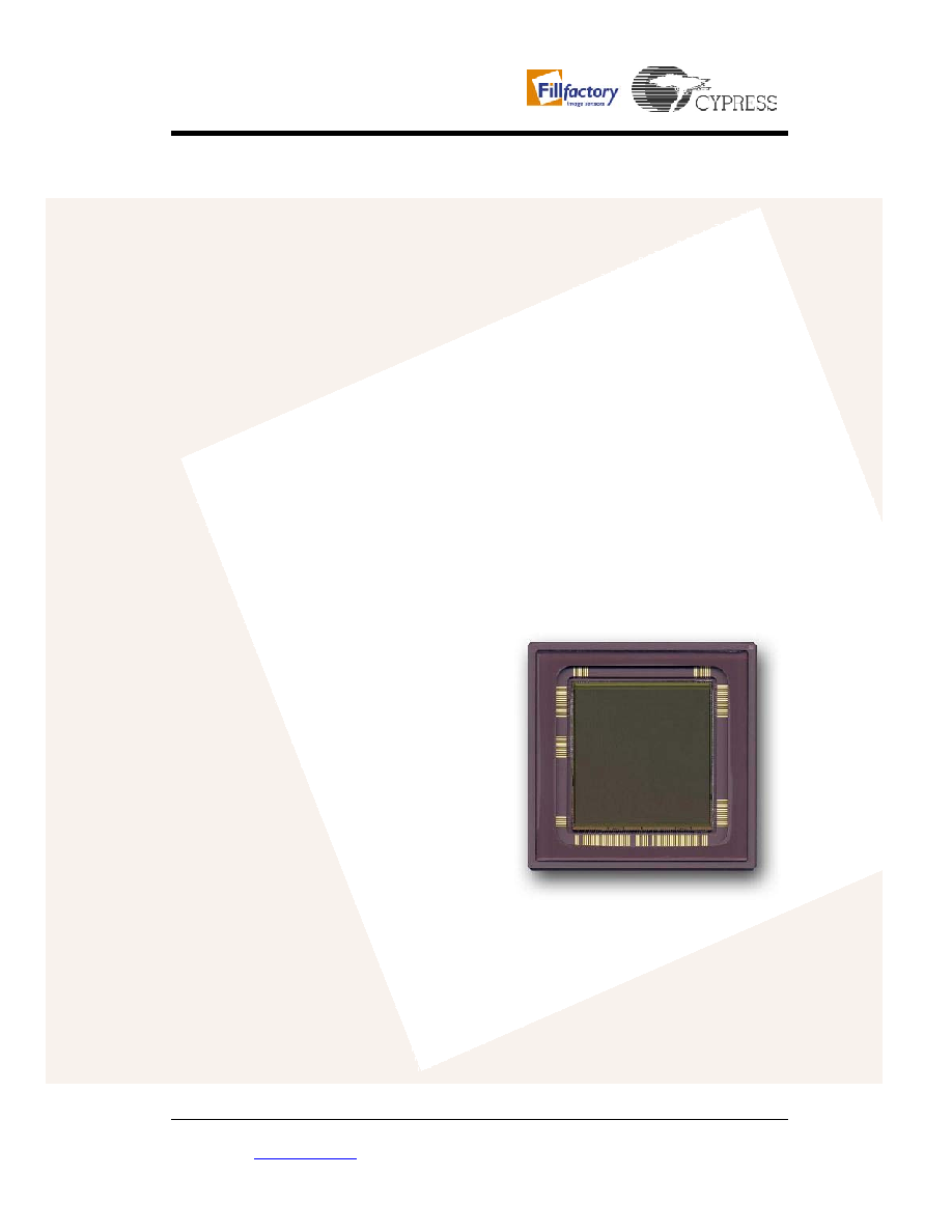
This document describes the interfacing and the driving of the LUPA-4000 image
sensor. This 4 mega-pixel CMOS active pixel sensor features synchronous shutter and
a maximal frame-rate of 15fps in full resolution. The readout speed can be boosted by
means of sub sampling and windowed Region Of Interest (ROI) readout. High
dynamic range scenes can be captured using the double and multiple slope
functionality.
The sensor can be used with one or two outputs. Two on chip 10-bit ADC's can be
used to convert the analog data to a 10-bit digital word stream. The sensor uses a 3-
wire Serial-Parallel (SPI) interface. It is housed in a 127-pin ceramic PGA package.
This datasheet allows the user to develop a camera-system based on the described
timing and interfacing.
1.2 Main
features
The main features of the image sensor are identified as:
· 2048 x 2048 active pixels (4M pixel resolution).
· 12
µm
2
square pixels (based on the high-fill factor active pixel sensor
technology of FillFactory (US patent No. 6,225,670 and others)).
· Peak QE x FF of 37.50%.
· Optical format: 24,6 mm x 24,6 mm
· Pixel rate of 66 MHz using a 33 MHz system clock.
· Optical dynamic range: 66 dB (2000:1) in single slope operation and up to 90
dB in multiple slope operation.
· 2 On-chip 10 bit, 33 MSamples/s ADC.
· Full snapshot shutter.
· Random programmable windowing and sub-sampling modes.
· 127-pin PGA package
· Binning (Voltage averaging in X-direction)
· Programmable read out direction (X and Y)
1.3 Part
Number
Name
Package
Monochrome / color
LUPA-4000-M
CYIL1SM4000AA-GBC (preliminary)
127 pin
ceramic PGA
Monochrome