 | –≠–ª–µ–∫—Ç—Ä–æ–Ω–Ω—ã–π –∫–æ–º–ø–æ–Ω–µ–Ω—Ç: W155 | –°–∫–∞—á–∞—Ç—å:  PDF PDF  ZIP ZIP |

Spread Spectrum Frequency Timing Generator
W155
Cypress Semiconductor Corporation
∑
3901 North First Street
∑
San Jose
∑
CA 95134
∑
408-943-2600
September 29, 1999, rev. **
Features
∑ Generates a spread spectrum timing signal (SYSCLK)
and a non-spread signal (USBCLK)
∑ Requires a 14.318-MHz crystal for operation
∑ Supports MIPS microprocessor clock frequencies
∑ Reduces peak EMI by as much as 12 dB
∑ Integrated loop filter components
∑ Cycle-to-cycle jitter = 250 ps (max)
∑ Operates with a 3.3 or 5.0V power supply
∑ Spread output is selectable from 10 to 133 MHz
∑ TEST mode supports modulation off (High-Z) and spe-
cial test input reference frequency
∑ Guaranteed 45/55 duty cycle
∑ Packaged in a 16-pin, 300-mil-wide SOIC (Small Outline
Integrated Circuit)
Overview
The W155 incorporates the latest advances in PLL-based
spread spectrum frequency synthesizer technology. By fre-
quency modulating the SYSCLK output with a low-frequency
carrier, peak EMI can be greatly reduced in a system. Use of
this technique allows systems to pass increasingly difficult EMI
testing without resorting to costly shielding or redesign.
In a system that uses the W155, not only is EMI reduced in the
various clock lines, but also in all signals which are synchro-
nized to SYSCLK. Therefore, the benefits of using this tech-
nique increase with the number of address and data lines in
the system.
The W155 is specifically targeted toward MIPS microproces-
sor based systems where EMI is of particular concern. Each
device uses a single 14.318-MHz crystal to generate a select-
able spread spectrum output and an unmodulated 48-MHz
USB Output.
The spreading function can be disabled by taking the SSON#
pin high. Spread percentage can be selected with the SS%
input (see Table 2 below).
Table 1. Frequency Selection (14.318-MHz Reference)
FS3
FS2
FS1
FS0
SYSCLK
(Output Freq.)
0
0
0
0
133.3 MHz
0
0
0
1
120 MHz
0
0
1
0
100 MHz
0
0
1
1
74.77 MHz
0
1
0
0
70 MHz
0
1
0
1
66.6 MHz
0
1
1
0
60 MHz
0
1
1
1
50 MHz
1
0
0
0
40 MHz
1
0
0
1
33.33 MHz
1
0
1
0
30 MHz
1
0
1
1
25 MHz
1
1
0
0
20 MHz
1
1
0
1
16.67 MHz
1
1
1
0
12 MHz
1
1
1
1
10 MHz
Table 2. Spread Percentage Selection
SS%
Spread Percentage
0
≠1.25%
1
≠3.75%
Pin Configuration
TEST
VDD
USBCLK/SS%*
GND
SYSCLK
GND
FS0*
SSON#^
16
15
14
13
12
11
10
9
VDD
X1
X2
GND
FS3*
VDD
FS2*
FS1*
1
2
3
4
5
6
7
8
W1
5
5
[1]
Note:
1.
Internal pull-up resistor present on inputs marked with `*' and pull-down
resistor present on input marked with `^'.

W155
2
Pin Definitions
Pin Name
Pin No.
Pin Type
Pin Description
USBCLK/
SS%
14
I/O
USB Clock Output/Modulation Width Selection Input: When an input; if spread
spectrum feature is enabled, this pin is used to select the amount of frequency
variation on the SYSCLK output (see Table 2). Wider variations result in greater
peak EMI reduction. When an output: supplies a non-spread 48-MHz signal for
USB support.
SYSCLK
12
O
System Clock Output: Frequency is selected per Table 1. Spread spectrum fea-
ture is controlled by pins 9 & 14.
FS0:3
10, 8, 7, 5
I
Frequency Select Pins: These pins set the frequency of the signal provided at
the SYSCLK output.
SSON#
9
I
Spread Spectrum Control (active LOW): Pulling this input signal HIGH turns the
internal modulating waveform off. This pin has an internal pull-down resistor.
X1
2
I
Crystal Connection or External Reference Frequency Input: This pin has dual
functions. It can be used as either an external crystal connection, or as an external
reference frequency input.
X2
3
I
Crystal Connection: If using an external reference, this pin must be left uncon-
nected.
TEST
16
I
Test Mode: For normal operation, tie this pin to ground.
VDD
1, 6, 15
P
Power Connection: Connected to either 3.3V or 5.0V power supply. All VDD pins
must be the same voltage level.
GND
4, 11, 13
G
Ground Connection: Connect to the common system ground plane.

W155
3
Functional Description
I/O Pin Operation
Pin 14 is a dual purpose l/O pin.
Upon power-up each I/O pin acts as a logic input, allowing the
determination of assigned device functions. A short time after
power-up, the logic state of each pin is latched and each pin
then becomes a clock output. This feature reduces device pin
count by combining clock outputs with input select pins.
An external 10-k
"strapping" resistor is connected between
each l/O pin and ground or V
DD
. Connection to ground sets a
"0" bit, connection to V
DD
sets a "1" bit. See Figure 1.
Upon W155 power-up, the first 2 ms of operation is used for
input logic selection. During this period, each clock output buff-
er is three-stated, allowing the output strapping resistor on
each l/O pin to pull the pin and its associated capacitive clock
load to either a logic HIGH or LOW state. At the end of the
2-ms period, the established logic 0 or 1 condition of each l/O
pin is then latched. Next the output buffer is enabled converting
all l/O pins into operating clock outputs. The 2-ms timer starts
when V
DD
reaches 2.0V. The input bits can only be reset by
turning V
DD
off and then back on again.
It should be noted that the strapping resistors have no signifi-
cant effect on clock output signal integrity. The drive imped-
ance of the clock outputs is <40
(nominal) which is minimally
affected by the 10-k
strap to ground or V
DD
. As with the se-
ries termination resistor, the output strapping resistor should
be placed as close to the l/O pin as possible in order to keep
the interconnecting trace short. The trace from the resistor to
ground or V
DD
should be kept less than two inches in length to
prevent system noise coupling during input logic sampling.
When each clock output is enabled following the 2-ms input
period, target (normal) output frequency is delivered assuming
that V
DD
has stabilized. If V
DD
has not yet reached full value,
output frequency initially may be below target but will increase
to target once V
DD
voltage has stabilized. In either case, a
short output clock cycle may be produced from the CPU clock
outputs when the outputs are enabled.
Output Buffer Configuration
Clock Outputs
All clock outputs are designed to drive serial terminated clock
lines. The device outputs are CMOS-type which provide
rail-to-rail output swing.
Crystal Oscillator
The device requires one input reference clock to synthesize all
output frequencies. The reference clock can be either an ex-
ternally generated clock signal or the clock generated by the
internal crystal oscillator. When using an external clock signal,
pin X1 is used as the clock input and pin X2 is left open. The
input threshold voltage of pin X1 is (V
DD
)/2.
The internal crystal oscillator is used in conjunction with a
quartz crystal connected to device pins X1 and X2. This forms
a parallel resonant crystal oscillator circuit. The device incor-
porates the necessary feedback resistor and crystal load ca-
pacitors. Including typical stray circuit capacitance, the total
load presented to the crystal is approximately 20 pF. For opti-
mum frequency accuracy without the addition of external ca-
pacitors, a parallel-resonant mode crystal specifying a load of
20 pF should be used. This will typically yield reference fre-
quency accuracies within ±100 ppm. To achieve similar accu-
racies with a crystal calling for a greater load, external capac-
itors must be added such that the total load (internal, external,
and parasitic capacitors) equals that called for by the crystal.
Power-on
Reset
Timer
Output Three-state
Data
Latch
Hold
Q
D
W155
V
DD
Clock Load
R
10 k
Output
Buffer
Output
Low
Output Strapping Resistor
Series Termination Resistor
Jumper Options
Figure 1. Input Logic Selection Through Jumper Option
W155
4
Spread Spectrum Frequency Timing Generator
The device generates a clock that is frequency modulated in
order to increase the bandwidth that it occupies. By increasing
the bandwidth of the fundamental and its harmonics, the am-
plitudes of the radiated electromagnetic emissions are re-
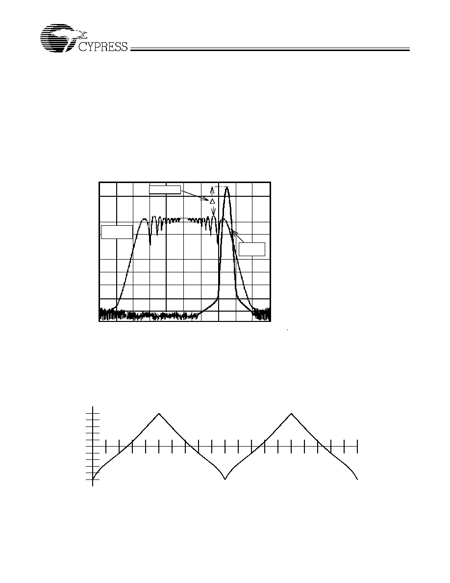
duced. This effect is depicted in Figure 2.
As shown in Figure 2, a harmonic of a modulated clock has a
much lower amplitude than that of an unmodulated signal. The
reduction in amplitude is dependent on the harmonic number
and the frequency deviation or spread. The equation for the
reduction is
dB = 6.5 + 9*log
10
(P) + 9*log
10
(F)
Where P is the percentage of deviation and F is the frequency
in MHz where the reduction is measured.
The output clock is modulated with a waveform depicted in
Figure 3. This waveform, as discussed in "Spread Spectrum
Clock Generation for the Reduction of Radiated Emissions" by
Bush, Fessler, and Hardin produces the maximum reduction
in the amplitude of radiated electromagnetic emissions. The
deviation selected for this chip is specified in Table 2. Figure 3
details the Cypress spreading pattern. Cypress does offer op-
tions with more spread and greater EMI reduction. Contact
your local sales representative for details on these devices.
Spread Spectrum clocking is activated or deactivated by se-
lecting the appropriate values for pin 9.
Spread
Spectrum
Enabled
EMI Reduction
Spread
Spectrum
Non-
Figure 2. Clock Harmonic with and without SSCG Modulation Frequency Domain Representation
MAX
MIN
10%
20%
30%
40%
50%
60%
70%
80%
90%
100%
10%
20%
30%
40%
50%
60%
70%
80%
90%
100%
FREQUENCY
Figure 3. Typical Modulation Profile
W155
5
Absolute Maximum Ratings
Stresses greater than those listed in this table may cause per-
manent damage to the device. These represent a stress rating
only. Operation of the device at these or any other conditions
above those specified in the operating sections of this specifi-
cation is not implied. Maximum conditions for extended peri-
ods may affect reliability
.
Document #: 38-00785
Parameter
Description
Rating
Unit
V
DD
, V
IN
Voltage on any pin with respect to GND
≠0.5 to +7.0
V
T
STG
Storage Temperature
≠65 to +150
∞C
T
A
Operating Temperature
0 to +70
∞C
T
B
Ambient Temperature under Bias
≠55 to +125
∞C
DC Electrical Characteristics:
0∞C < T
A
< 70∞C, V
DD
= 3.30V±10%
Parameter
Description
Test Condition
Min
Typ
Max
Unit
I
DD
Supply Current
35
mA
V
IL
Input Low Voltage
0.8
V
V
IH
Input High Voltage
2.0
V
V
OL
Output Low Voltage
I
OL
= 2 mA
50
mV
V
OH
Output High Voltage
I
OH
= ≠2 mA
3.10
V
I
OL
Output Low Current
V
OL
= 1.5V
80
110
155
mA
I
OH
Output High Current
V
OH
= 1.5V
80
120
175
mA
I
IL
Input Low Current
10
µ
A
I
IH
Input High Current
10
µ
A
C
I
Input Capacitance
5
10
pF
C
L
XTAL Load Capacitance
20
pF
Switching Characteristics
Parameter
Description
Test Conditions
Min
Typ
Max
Unit
t
TLH
, t
THL
Output Rise and Fall Time measured
at 10% of 90% of V
DD
0.8
4.0
ns
t
TLH,
t
THL
Output Rise and Fall Time measured
at 0.8V≠2.0V
0.3
1.0
ns
t
SYM
Output Duty Cycle
45
55
%
t
JCC
Cycle-to-Cycle Jitter
250
ps
EMI
EMI Attenuation
11th Harmonic, 25 MHz
10
dB
Ordering Information
Ordering Code
Package
Name
Package Type
W155
G
16-pin Plastic SOIC (300-mil, wide body)