 | –≠–ª–µ–∫—Ç—Ä–æ–Ω–Ω—ã–π –∫–æ–º–ø–æ–Ω–µ–Ω—Ç: W161 | –°–∫–∞—á–∞—Ç—å:  PDF PDF  ZIP ZIP |

PRELIMINARY
133-MHz Spread Spectrum FTG for PentiumÆ II Platforms
W161
Cypress Semiconductor Corporation
∑
3901 North First Street
∑
San Jose
∑
CA 95134
∑
408-943-2600
October 13, 1999, rev. **
Features
∑ Maximized EMI Suppression using Cypress's Spread
Spectrum Technology
∑ Three copies of CPU outputs at 100 or 133 MHz
∑ Three copies of 66-MHz output at 3.3V
∑ Ten copies of PCI clocks at 33 MHz, 3.3V
∑ Two copies of 14.318-MHz reference output at 3.3V
∑ One copy of 48-MHz USB clock
∑ One copy of CPU-divide-by-2 output as reference input
to Direct RambusTM Clock Generator (Cypress W134)
∑ Available in 48-pin SSOP (300 mils)
Key Specifications
Supply Voltages: ...................................... V
DDQ2
= 2.5V±5%
V
DDQ3
= 3.3V±5%
CPU, CPUdiv2 Output Jitter:....................................... 250 ps
CPU, CPUdiv2 Output Skew: ...................................... 175 ps
IOAPIC, 3V66 Output Skew: ....................................... 250 ps
PCI0:9 Output Skew: .................................................. 500 ps
Duty Cycle: ................................................................... 45/55
Spread Spectrum Modulation:..................................... ≠0.5%
CPU to 3V66 Output Offset: ............. 0.0≠1.5 ns (CPU leads)
3V66 to PCI Output Offset:.............. 1.5≠3.0 ns (3V66 leads)
CPU to IOAPIC Output Offset: ......... 1.5≠4.0 ns (CPU leads)
Pentium is a registered trademark of Intel Corporation. Direct Rambus is a trademark of Rambus, Inc.
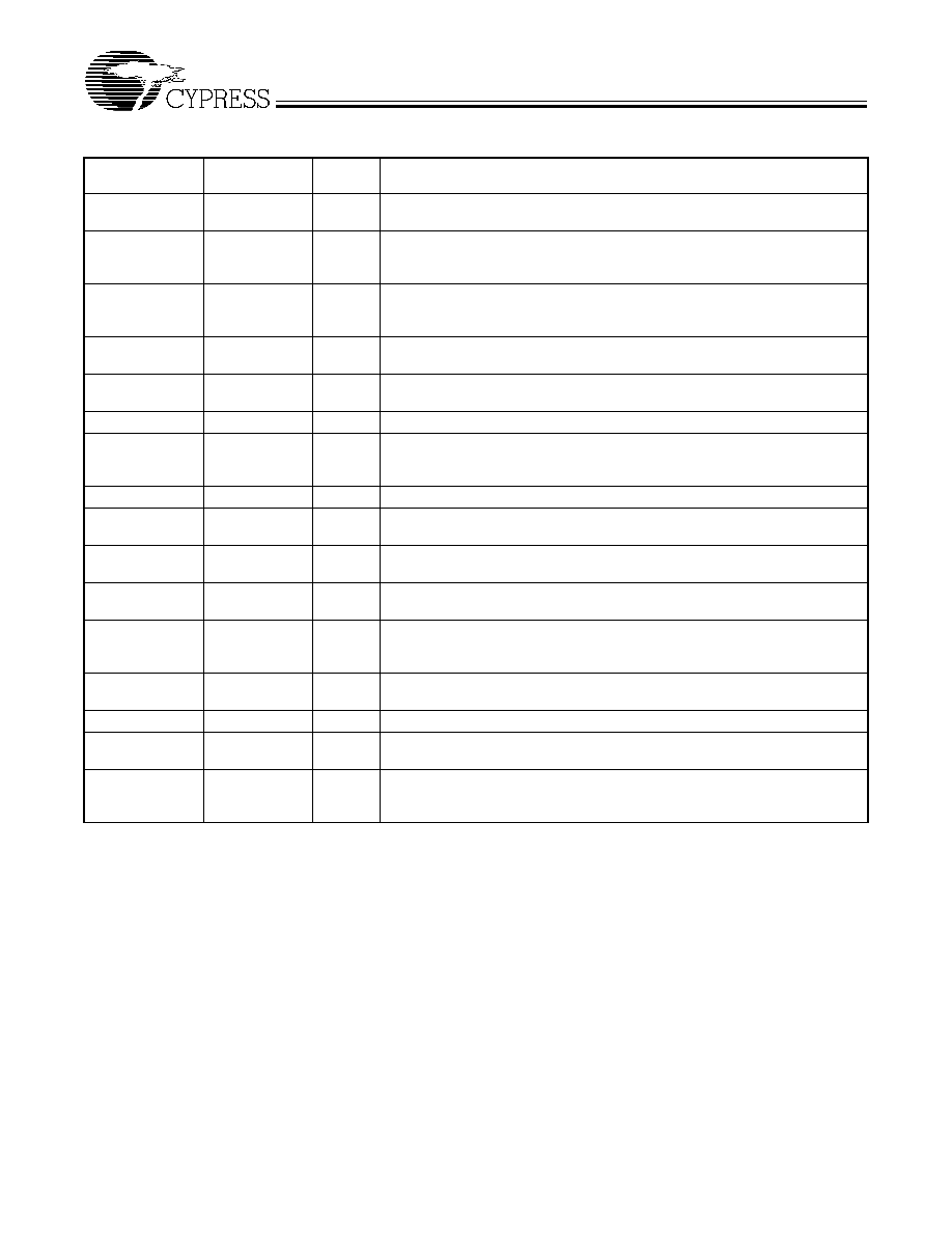
Table 1. Pin Selectable Frequency
SEL133/100#
SEL1
SEL0
Function
0
0
0
All outputs Three-State
0
0
1
(Reserved)
0
1
0
Active 100-MHz, 48-MHz
PLL inactive
0
1
1
Active 100-MHz, 48-MHz
PLL active
1
0
0
Test Mode
1
0
1
(Reserved)
1
1
0
Active 133-MHz, 48-MHz
PLL inactive
1
1
1
Active 133-MHz, 48-MHz
PLL active
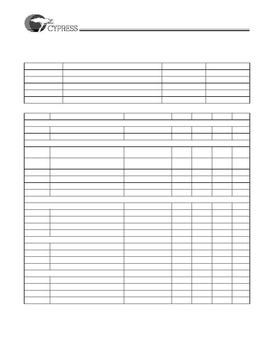
Block Diagram
Pin Configuration
REF_[0:1]
CPU_[0:2]
CPUdiv2
3V66_[0:2]
XTAL
PLL 1
SPREAD#
X2
X1
PCI_[0:9]
IOAPIC
48MHz
PLL2
OSC
˜2
Power
Three-state
Logic
SEL0
SEL1
SEL133/100#
˜2/˜1.5
Down
Logic
˜2
˜2
2
3
3
9
PWRDWN#
REF0
REF1
VDDQ3
X1
X2
GND
PCI0
PCI1
VDDQ3
PCI2
PCI3
PCI4
PCI5
GND
PCI6
PCI7
VDDQ3
PCI8
PCI9
GND
3V66_0
3V66_1
3V66_2
VDDQ3
W1
61
GND
VDDQ2
IOAPIC
GND
VDDQ2
CPUdiv2
GND
VDDQ2
CPU2
GND
VDDQ2
CPU1
CPU0
GND
VDDQ3
GND
PWRDWN#*
SPREAD#*
SEL1*
SEL0*
VDDQ3
48MHz
GND
SEL133/100#
48
47
46
45
44
43
42
41
40
39
38
37
36
35
34
33
32
31
30
29
28
27
26
25
1
2
3
4
5
6
7
8
9
10
11
12
13
14
15
16
17
18
19
20
21
22
23
24
Note:
1.
Internal 250-k
pull-up resistors present on inputs marked with *.
Design should not rely solely on internal pull-up resistor to set I/O
pins HIGH.
[1]
W161
PRELIMINARY
2
Overview
The W161, a motherboard clock synthesizer, provides 2.5V
CPU clock outputs for advanced CPU and a CPU-divide-by-2
reference frequency for Direct Rambus
Clock Generator (such
Cypress W134) interface. Fixed output frequencies are provid-
ed for other system functions.
CPU Frequency Selection
CPU frequency is selected with input pins 25, 29, and 30
(SEL133/100#, SEL0, and SEL1, respectively). Refer to Table
1 for details.
Output Buffer Configuration
Clock Outputs
All clock outputs are designed to drive serial terminated clock
lines. The W161 outputs are CMOS-type, which provide
rail-to-rail output swing.
Crystal Oscillator
The W161 requires one input reference clock to synthesize all
output frequencies. The reference clock can be either an ex-
ternally generated clock signal or the clock generated by the
internal crystal oscillator. When using an external clock signal,
pin X1 is used as the clock input and pin X2 is left open.
The internal crystal oscillator is used in conjunction with a
quartz crystal connected to device pins X1 and X2. This forms
a parallel resonant crystal oscillator circuit. The W161 incor-
porates the necessary feedback resistor and crystal load ca-
pacitors. Including typical stray circuit capacitance, the total
load presented to the crystal is approximately 18 pF. For opti-
mum frequency accuracy without the addition of external ca-
pacitors, a parallel-resonant mode crystal specifying a load of
18 pF should be used. This will typically yield reference fre-
quency accuracies within ±100 ppm.
Pin Definitions
Pin Name
Pin
No.
Pin
Type
Pin Description
CPU0:2
36, 37, 40
O
CPU Clock Outputs 0 through 2: CPU clock outputs. Their output voltage
swing is controlled by voltage applied to VDDQ2.
PCI0:9
7, 8, 10, 11, 12,
13, 15, 16, 18,
19
O
PCI Clock Outputs 0 through 9: Output voltage swing is controlled by voltage
applied to VDDQ3.
CPUdiv2
43
O
CPU-Divide-By-2 Output: This serves as a reference input signal for Direct
Rambus Clock Generator (Cypress W134). The output voltage is determined
by VDDQ2.
3V66_0:2
21, 22, 23
O
66-MHz Clock Outputs 0 through 2: Output voltage swing is controlled by
voltage applied to VDDQ3.
IOAPIC
46
O
I/O APIC Clock Output: Provides an output synchronous to CPU clock. See
Table 1 for their relation to other system clock outputs.
48 MHz
27
O
48-MHz Output: Fixed clock output at 48 MHz.
SPREAD#
31
I
Spread Spectrum Enable: This input enables spread spectrum modulation
on the PLL1 generated frequency outputs of the W161. Modulation range is
≠0.5%.
PWRDWN#
32
I
Power Down Control
REF0:1
1, 2
I
Fixed 14.318-MHz Output 0 and 1: Output voltage swing is controlled by
voltage applied to VDDQ3.
SEL0:1
29, 30
I
Mode Select Input 0 through 1: 3.3V LVTTL-compatible input for selecting
clock output modes. As shown in Table 1.
SEL133/100#
25
I
Frequency Selection Input: 3.3V LVTTL-compatible input that selects CPU
output frequency as shown in Table 1.
X1
4
I
Crystal Connection or External Reference Frequency Input: This pin has
dual functions. It can be used as an external 14.318-MHz crystal connection
or as an external reference frequency input.
X2
5
I
Crystal Connection: An input connection for an external 14.318-MHz crystal.
If using an external reference, this pin must be left unconnected.
VDDQ2
38, 41, 44, 47
P
Power Connection: Connected to 2.5V power supply.
VDDQ3
3, 9, 17, 24, 28,
34
P
Power Connection: Connected to 3.3V power supply.
GND
6, 14, 20, 26,
33, 35, 39, 42,
45, 48
G
Ground Connection: Connect all ground pins to the common system ground
plane.

W161
PRELIMINARY
3
Spread Spectrum Feature
The device generates a clock that is frequency modulated in
order to increase the bandwidth that it occupies. By increasing
the bandwidth of the fundamental and its harmonics, the am-
plitudes of the radiated electromagnetic emissions are re-
duced. This effect is depicted in Figure 1.
As shown in Figure 1, a harmonic of a modulated clock has a
much lower amplitude than that of an unmodulated signal. The
reduction in amplitude is dependent on the harmonic number
and the frequency deviation or spread. The equation for the
reduction is
dB = 6.5 + 9*log
10
(P) + 9*log
10
(F)
Where P is the percentage of deviation and F is the frequency
in MHz where the reduction is measured.
The output clock is modulated with a waveform depicted in
Figure 2. This waveform, as discussed in "Spread Spectrum
Clock Generation for the Reduction of Radiated Emissions" by
Bush, Fessler, and Hardin produces the maximum reduction
in the amplitude of radiated electromagnetic emissions. The
deviation selected for this chip is ≠0.5% downspread. Figure 2
details the Cypress spreading pattern. Cypress does offer op-
tions with more spread and greater EMI reduction. Contact
your local Sales representative for details on these devices.
Spread
Spectrum
Enabled
EMI Reduction
Spread
Spectrum
Non-
Figure 1. Typical Clock and SSFTG Comparison
100%
60%
20%
80%
40%
0%
≠20%
≠40%
≠60%
≠80%
≠100%
10
%
20
%
30
%
40
%
50
%
60
%
70
%
80
%
90
%
10
0%
10
%
20
%
30
%
40
%
50
%
60
%
70
%
80
%
90
%
10
0%
Time
Fr
e
que
ncy
Sh
i
f
t
Figure 2. Typical Modulation Profile
W161
PRELIMINARY
4
Absolute Maximum Ratings
Stresses greater than those listed in this table may cause per-
manent damage to the device. These represent a stress rating
only. Operation of the device at these or any other conditions
above those specified in the operating sections of this specifi-
cation is not implied. Maximum conditions for extended peri-
ods may affect reliability.
.
Parameter
Description
Rating
Unit
V
DD
, V
IN
Voltage on any pin with respect to GND
≠0.5 to +7.0
V
T
STG
Storage Temperature
≠65 to +150
∞C
T
A
Operating Temperature
0 to +70
∞C
T
B
Ambient Temperature under Bias
≠55 to +125
∞C
ESD
PROT
Input ESD Protection
2 (min.)
kV
DC Electrical Characteristics:
T
A
= 0∞C to +70∞C, V
DDQ3
= 3.3V±5%, V
DDQ2
= 2.5V±5%
Parameter
Description
Test Condition
Min.
Typ.
Max.
Unit
Supply Current
I
DD-3.3V
Combined 3.3V Supply Current
CPU0:3 =133 MHz
[2]
160
mA
I
DD-2.5
Combined 2.5V Supply Current
CPU0:3 =133 MHz
[2]
90
mA
Logic Inputs (All referenced to V
DDQ3
= 3.3V)
V
IL
Input Low Voltage
GND ≠
0.3
0.8
V
V
IH
Input High Voltage
2.0
V
DD
+
0.3
V
I
IL
Input Low Current
[3]
≠25
µA
I
IH
Input High Current
[3]
10
µA
I
IL
Input Low Current, SEL133/100#
[3]
≠5
µA
I
IH
Input High Current, SEL133/100#
[3]
5
µA
Clock Outputs
CPU, CPUdiv2, IOAPIC (Referenced to V
DDQ2
)
Test Condition
Min.
Typ.
Max.
Unit
V
OL
Output Low Voltage
I
OL
= 1 mA
50
mV
V
OH
Output High Voltage
I
OH
= ≠1 mA
2.2
V
I
OL
Output Low Current
V
OL
= 1.25V
45
65
100
mA
I
OH
Output High Current
V
OH
= 1.25V
45
65
100
mA
48MHz, REF (Referenced to V
DDQ3
)
Test Condition
Min.
Typ.
Max.
Unit
V
OL
Output Low Voltage
I
OL
= 1 mA
50
mV
V
OH
Output High Voltage
I
OH
= ≠1 mA
3.1
V
I
OL
Output Low Current
V
OL
= 1.5V
45
65
100
mA
I
OH
Output High Current
V
OH
= 1.5V
45
65
100
mA
PCI, 3V66 (Referenced to V
DDQ3
)
Test Condition
Min.
Typ.
Max.
Unit
V
OL
Output Low Voltage
I
OL
= 1 mA
50
mV
V
OH
Output High Voltage
I
OH
= ≠1 mA
3.1
V
I
OL
Output Low Current
V
OL
= 1.5V
70
100
145
mA
I
OH
Output High Current
V
OH
= 1.5V
65
95
135
mA
Notes:
2.
All clock outputs loaded with 6" 60
transmission lines with 20-pF capacitors.
3.
W161 logic inputs have internal pull-up devices, except SEL133/100# (pull-ups not CMOS level).

W161
PRELIMINARY
5
3.3V AC Electrical Characteristics
T
A
= 0∞C to +70∞C, V
DDQ3
= 3.3V±5%,V
DDQ2
= 2.5V± 5%, f
XTL
= 14.31818 MHz
Spread Spectrum function turned off
AC clock parameters are tested and guaranteed over stated operating conditions using the stated lump capacitive load at the
clock output.
[7]
Notes:
4.
X1 input threshold voltage (typical) is V
DD
/2.
5.
The W161 contains an internal crystal load capacitor between pin X1 and ground and another between pin X2 and ground. Total load placed on crystal is 18 pF;
this includes typical stray capacitance of short PCB traces to crystal.
6.
X1 input capacitance is applicable when driving X1 with an external clock source (X2 is left unconnected).
7.
Period, jitter, offset, and skew measured on rising edge at 1.5V.
8.
3V66 is CPU/2 for CPU =133 MHz and (2 x CPU)/3 for CPU = 100 MHz.
Crystal Oscillator
V
TH
X1 Input threshold Voltage
[4]
1.65
V
C
LOAD
Load Capacitance, Imposed on
External Crystal
[5]
18
pF
C
IN,X1
X1 Input Capacitance
[6]
Pin X2 unconnected
28
pF
Pin Capacitance/Inductance
C
IN
Input Pin Capacitance
Except X1 and X2
5
pF
C
OUT
Output Pin Capacitance
6
pF
L
IN
Input Pin Inductance
7
nH
DC Electrical Characteristics:
T
A
= 0∞C to +70∞C, V
DDQ3
= 3.3V±5%, V
DDQ2
= 2.5V±5% (continued)
Parameter
Description
Test Condition
Min.
Typ.
Max.
Unit
3V66 Clock Outputs, 3V66_0:3 (Lump Capacitance Test Load = 30 pF)
Parameter
Description
Test Condition/Comments
Min.
Typ.
Max.
Unit
f
Frequency
Note 8
66.6
MHz
t
R
Output Rise Edge Rate
Measured from 0.4V to 2.4V
1
4
V/ns
t
F
Output Fall Edge Rate
Measured from 2.4V to 0.4V
1
4
V/ns
t
D
Duty Cycle
Measured on rising and falling edge at 1.5V
45
55
%
f
ST
Frequency Stabilization
from Power-up (cold start)
Assumes full supply voltage reached within
1 ms from power-up. Short cycles exist prior
to frequency stabilization.
3
ms
Z
o
AC Output Impedance
Average value during switching transition.
Used for determining series termination
value.
15