 | –≠–ª–µ–∫—Ç—Ä–æ–Ω–Ω—ã–π –∫–æ–º–ø–æ–Ω–µ–Ω—Ç: W164G | –°–∫–∞—á–∞—Ç—å:  PDF PDF  ZIP ZIP |

Spread Spectrum Desktop/Notebook System
Frequency Generator
W164
Cypress Semiconductor Corporation
∑
3901 North First Street
∑
San Jose
∑
CA 95134
∑
408-943-2600
Document #: 38-07169 Rev. *A
Revised December 15, 2002
Features
∑ Maximized EMI suppression using Cypress's Spread
Spectrum technology
∑ Reduces measured EMI by as much as 10 dB
∑ I
2
C programmable to 153 MHz (16 selectable
frequencies)
∑ Two skew-controlled copies of CPU output
∑ SEL100/66# selects CPU frequency (100 or 66.8 MHz)
∑ Seven copies of PCI output (synchronous w/CPU
output)
∑ One copy of 14.31818-MHz IOAPIC output
∑ One copy of 48-MHz USB output
∑ Selectable 24-/48-MHz output is determined by resistor
straps on power-up
∑ One high-drive output buffer that produces a copy of
the 14.318-MHz reference
∑ Isolated core VDD pin for noise reduction
Key Specifications
Supply Voltages:....................................... V
DDQ3
= 3.3V±5%
V
DDQ2
= 2.5V±5%
CPU Cycle to Cycle Jitter: ........................................... 200 ps
CPU, PCI Output Edge Rate:
.........................................
1 V/ns
CPU0:1 Output Skew: ................................................ 175 ps
PCI_F, PCI1:6 Output Skew: ....................................... 500 ps
CPU to PCI Skew: .............................. 1 to 4 ns (CPU Leads)
REF2X/SEL48#, SCLOCK, SDATA................ 250-k
pull-up
Note: Internal pull-up resistors should not be relied upon for
setting I/O pins HIGH.
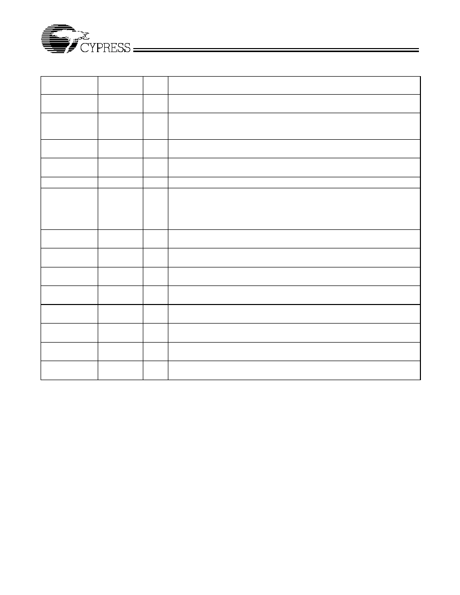
Table 1. Pin Selectable Frequency
SEL100/66#
CPU(0:1)
PCI
1
100 MHz
33.3 MHz
0
66.8 MHz
33.4 MHz
Pin Configuration
Block Diagram
X1
X2
GND
PCI_F
PCI1
PCI2
PCI3
PCI4
VDDQ3
PCI5
PCI6
VDDQ3
48MHz
24/48MHz
GND
REF2X/SEL48#
VDDQ3
VDDQ2
IOAPIC
VDDQ2
CPU0
CPU1
VDDQ3
GND
SDATA
SCLOCK
SEL100/66#
GND
28
27
26
25
24
23
22
21
20
19
18
17
16
15
1
2
3
4
5
6
7
8
9
10
11
12
13
14
VDDQ3
REF2X/SEL48#
VDDQ3
IOAPIC
CPU0
CPU1
PCI_F
XTAL
PLL Ref Freq
PLL 1
100/66#_SEL
X2
X1
VDDQ3
PCI1
PCI2
PCI3
PCI4
PCI5
48MHz
24/48MHz
PLL2
OSC
VDDQ2
PCI6
GND
GND
VDDQ3
GND
GND
I
2
C
SCLOCK
SDATA
LOGIC
˜2/˜3/˜4
W164
Document #: 38-07169 Rev. *A
Page 2 of 12
Functional Description
I/O Pin Operation
Pin 27 is a dual-purpose l/O pin. Upon power-up this pin acts
as a logic input, allowing the determination of assigned device
functions. A short time after power-up, the logic state of the pin
is latched and the pin becomes a clock output. This feature
reduces device pin count by combining clock outputs with in-
put select pins.
An external 10-k
"strapping" resistor is connected between
the l/O pin and ground or V
DD
. Connection to ground sets a
latch to "0," connection to V
DD
sets a latch to "1." Figure 1 and
Figure 2 show two suggested methods for strapping resistor
connections.
Upon W164 power-up, the first 2 ms of operation is used for
input logic selection. During this period, the Reference clock
output buffer is three-stated, allowing the output strapping re-
sistor on the l/O pin to pull the pin and its associated capacitive
clock load to either a logic HIGH or LOW state. At the end of
the 2-ms period, the established logic "0" or "1" condition of the
l/O pin is then latched. Next the output buffer is enabled which
converts the l/O pin into an operating clock output. The 2-ms
timer is started when V
DD
reaches 2.0V. The input bit can only
be reset by turning V
DD
off and then back on again.
It should be noted that the strapping resistor has no significant
effect on clock output signal integrity. The drive impedance of
clock output is 25
(nominal) which is minimally affected by
the 10-k
strap to ground or V
DD
. As with the series termina-
tion resistor, the output strapping resistor should be placed as
close to the l/O pin as possible in order to keep the intercon-
necting trace short. The trace from the resistor to ground or
V
DD
should be kept less than two inches in length to prevent
system noise coupling during input logic sampling.
When the clock output is enabled following the 2-ms input pe-
riod, a 14.318-MHz output frequency is delivered on the pin,
assuming that V
DD
has stabilized. If V
DD
has not yet reached
full value, output frequency initially may be below target but will
increase to target once V
DD
voltage has stabilized. In either
case, a short output clock cycle may be produced from the
CPU clock outputs when the outputs are enabled.
Pin Definitions
Pin Name
Pin
No.
Pin
Type
Pin Description
CPU0:1
22, 21
O
CPU Clock Outputs 0 through 1: These two CPU clocks run at a frequency set by
SEL100/66#. Output voltage swing is set by the voltage applied to VDDQ2.
PCI1:6
PCI_F
5, 6, 7, 8, 10,
11, 4
O
PCI Clock Outputs 1 through 6 and PCI_F: These seven PCI clock outputs run
synchronously to the CPU clock. Voltage swing is set by the power connection to
VDDQ3.
IOAPIC
24
O
I/O APIC Clock Output: Provides 14.318-MHz fixed frequency. The output voltage
swing is set by the power connection to VDDQ2.
48MHz
13
O
48-MHz Output: Fixed 48-MHz USB clock. Output voltage swing is controlled by
voltage applied to VDDQ3.
24/48MHz
14
O
24-MHz or 48-MHz Output: Frequency is set by the state of pin 27 on power-up.
REF2X/SEL48#
27
I/O
I/O Dual-Function REF2X and SEL48# pin: Upon power-up, the state of SEL48#
is latched. The initial state is set by either a 10K resistor to GND or to V
DD
. A 10K
resistor to GND causes pin 14 to output 48 MHz. If the pin is strapped to V
DD
, pin
14 will output 24 MHz. After 2 ms, the pin becomes a high-drive output that produces
a copy of 14.318 MHz.
SEL100/66# 16
I
Frequency Selection Input: Selects CPU clock frequency as shown in Table 1 on
page 1.
SDATA
18
I/O
I
2
C Data Pin: Data should be presented to this input as described in the I
2
C section
of this data sheet. Internal 250-k
pull-up resistor.
SCLOCK
17
I
I
2
C Clock Pin: The I
2
C data clock should be presented to this input as described in
the I
2
C section of this data sheet.
X1
1
I
Crystal Connection or External Reference Frequency Input: Connect to either
a 14.318-MHz crystal or other reference signal.
X2
2
I
Crystal Connection: An input connection for an external 14.318-MHz crystal. If
using an external reference, this pin must be left unconnected.
VDDQ3
9, 12, 20, 26
P
Power Connection: Power supply for core logic and PLL circuitry, PCI, 48-/24-MHz,
and Reference output buffers. Connect to 3.3V supply.
VDDQ2
23, 25
P
Power Connection: Power supply for IOAPIC and CPU output buffers. Connect to
2.5V supply.
GND
3, 15, 19, 28
G
Ground Connections: Connect all ground pins to the common system ground
plane.

W164
Document #: 38-07169 Rev. *A
Page 3 of 12
Serial Data Interface
The W164 features a two-pin, serial data interface that can be
used to configure internal register settings that control partic-
ular device functions. Upon power-up, the W164 initializes
with default register settings. Therefore, the use of this serial
data interface is optional. The serial interface is write-only (to
the clock chip) and is the dedicated function of device pins
SDATA and SCLOCK. In motherboard applications, SDATA
and SCLOCK are typically driven by two logic outputs of the
chipset. Clock device register changes are normally made
upon system initialization, if required. The interface can also
be used during system operation for power management func-
tions. Table 2 summarizes the control functions of the serial
data interface.
Operation
Data is written to the W164 in ten bytes of eight bits each.
Bytes are written in the order shown in Table 3.
Power-on
Reset
Timer
Output Three-state
Data
Latch
Hold
Q
D
W164
V
DD
Clock Load
10 k
Output
Buffer
(Load Option 1)
10 k
(Load Option 0)
Output
Low
Output Strapping Resistor
Series Termination Resistor
Figure 1. Input Logic Selection Through Resistor Load Option
Power-on
Reset
Timer
Output Three-state
Data
Latch
Hold
Q
D
W164
V
DD
Clock Load
R
10 k
Output
Buffer
Output
Low
Output Strapping Resistor
Series Termination Resistor
Jumper Options
Resistor Value R
Figure 2. Input Logic Selection Through Jumper Option
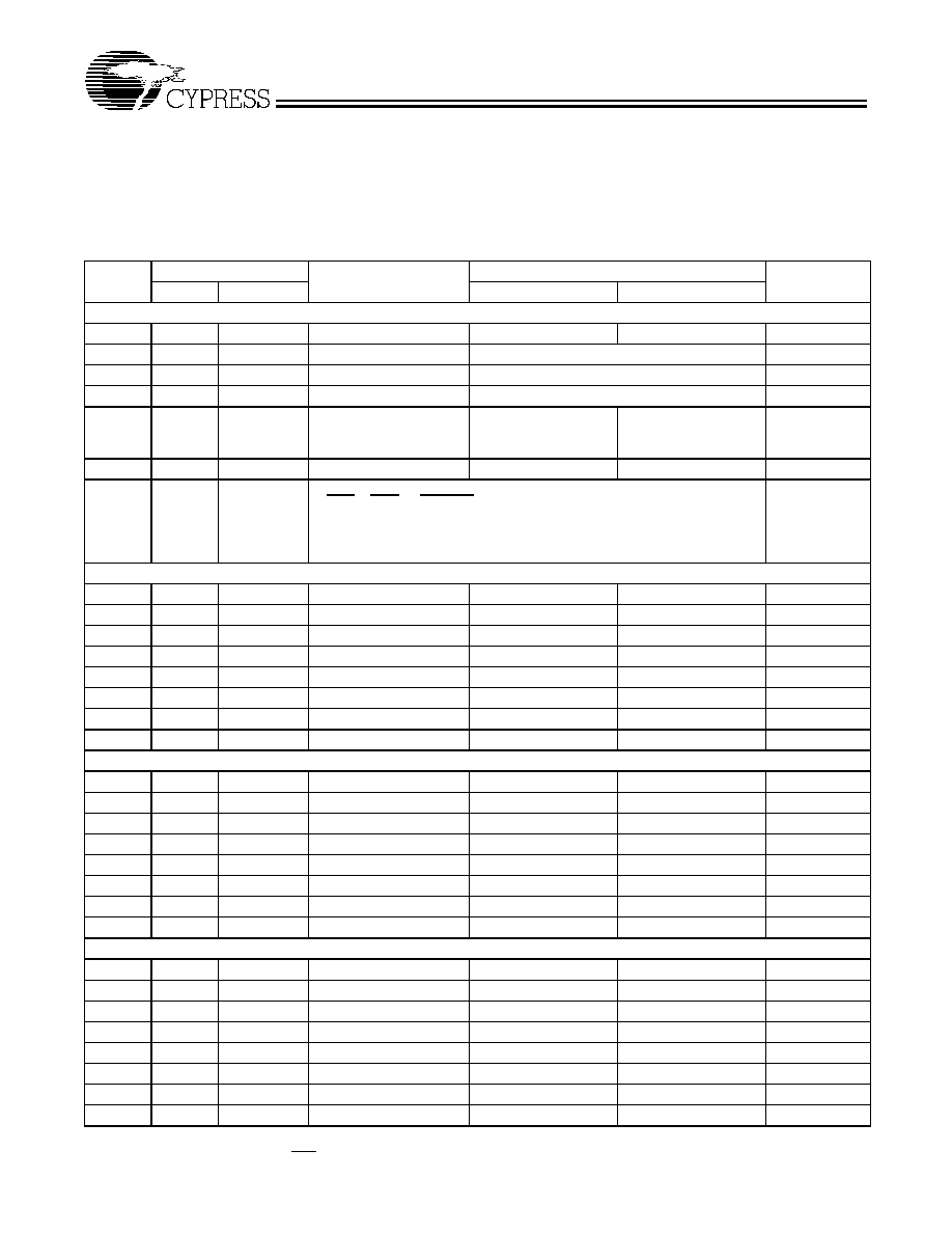
Table 2. Serial Data Interface Control Functions Summary
Control Function
Description
Common Application
Clock Output Disable
Any individual clock output(s) can be disabled. Dis-
abled outputs are actively held LOW.
Unused outputs are disabled to reduce EMI
and system power. Examples are clock out-
puts to unused PCI slots.
CPU Clock Frequency
Selection
Provides CPU/PCI frequency selections beyond the
100- and 66.6-MHz selections that are provided by
the SEL100/66# pin. Frequency is changed in a
smooth and controlled fashion.
For alternate microprocessors and power
management options. Smooth frequency tran-
sition allows CPU frequency change under
normal system operation.
Output Three-state
Puts all clock outputs into a high-impedance state.
Production PCB testing.
Test Mode
All clock outputs toggle in relation to X1 input, inter-
nal PLL is bypassed. Refer to Table 4.
Production PCB testing.
(Reserved)
Reserved function for future device revision or pro-
duction device testing.
No user application. Register bit must be writ-
ten as 0.

W164
Document #: 38-07169 Rev. *A
Page 4 of 12
Table 3. Byte Writing Sequence
Byte
Sequence
Byte Name
Bit Sequence
Byte Description
1
Slave Address
11010010
Commands the W164 to accept the bits in Data Bytes 3≠6 for internal
register configuration. Since other devices may exist on the same com-
mon serial data bus, it is necessary to have a specific slave address for
each potential receiver. The slave receiver address for the W164 is
11010010. Register setting will not be made if the Slave Address is not
correct (or is for an alternate slave receiver).
2
Command
Code
Don't Care
Unused by the W164, therefore bit values are ignored ("don't care"). This
byte must be included in the data write sequence to maintain proper byte
allocation. The Command Code Byte is part of the standard serial com-
munication protocol and may be used when writing to another addressed
slave receiver on the serial data bus.
3
Byte Count
Don't Care
Unused by the W164, therefore bit values are ignored ("don't care"). This
byte must be included in the data write sequence to maintain proper byte
allocation. The Byte Count Byte is part of the standard serial communi-
cation protocol and may be used when writing to another addressed slave
receiver on the serial data bus.
4
Data Byte 0
Don't Care
Refer to Cypress SDRAM drivers.
5
Data Byte 1
6
Data Byte 2
7
Data Byte 3
Refer to Table 4
The data bits in these bytes set internal W164 registers that control device
operation. The data bits are only accepted when the Address Byte bit
sequence is 11010010, as noted above. For description of bit control
functions, refer to Table 4, Data Byte Serial Configuration Map.
8
Data Byte 4
9
Data Byte 5
10
Data Byte 6
W164
Document #: 38-07169 Rev. *A
Page 5 of 12
Writing Data Bytes
Each bit in the data bytes controls a particular device function
except for the "reserved" bits, which must be written as a logic
0. Bits are written MSB (most significant bit) first, which is bit
7. Table 4 gives the bit formats for registers located in Data
Bytes 3≠6.
Table 5 details additional frequency selections that are avail-
able through the serial data interface.
Table 6 details the select functions for Byte 3, bits 1 and 0.
Note:
1.
Both Bits 0 and 1 of Byte 6 in Table 4 must be programmed as the same value.
Table 4. Data Bytes 3≠6 Serial Configuration Map
Bit(s)
Affected Pin
Control Function
Bit Control
Default
Pin No.
Pin Name
0
1
Data Byte 3
7
--
--
SEL_3
--
--
0
6
--
--
SEL_2
Refer to Table 5
0
5
--
--
SEL_1
Refer to Table 5
0
4
--
--
SEL_0
Refer to Table 5
0
3
--
--
Frequency Table
Selection
Frequency Controlled
by external SEL100/
66# pin Table 1
Frequency Controlled
by BYT3 SEL_(3:0)
Table 5
0
2
--
--
(Reserved)
--
--
0
1≠0
--
--
Bit 1
Bit 0
Function (See Table 6 for function details)
0
0
Normal Operation
0
1
Test Mode
1
0
Spread Spectrum on
1
1
All Outputs Three-stated
00
Data Byte 4
7
--
--
(Reserved)
--
--
0
6
14
24/48MHz
Clock output Disable
Low
Active
1
5
--
--
(Reserved)
--
--
0
4
--
--
(Reserved)
--
--
0
3
--
--
(Reserved)
--
--
0
2
21
CPU1
Clock Output Disable
Low
Active
1
1
--
--
(Reserved)
--
--
0
0
22
CPU0
Clock Output Disable
Low
Active
1
Data Byte 5
7
4
PCI_F
Clock Output Disable
Low
Active
1
6
11
PCI6
Clock Output Disable
Low
Active
1
5
10
PCI5
Clock Output Disable
Low
Active
1
4
-
--
(Reserved)
--
--
0
3
8
PCI4
Clock Output Disable
Low
Active
1
2
7
PCI3
Clock Output Disable
Low
Active
1
1
6
PCI2
Clock Output Disable
Low
Active
1
0
5
PCI1
Clock Output Disable
Low
Active
1
Data Byte 6
7
--
--
(Reserved)
--
--
0
6
--
--
(Reserved)
--
--
0
5
24
IOAPIC
Clock Output Disable
Low
Active
1
4
--
--
(Reserved)
--
--
0
3
--
--
(Reserved)
--
--
0
2
--
--
(Reserved)
--
--
0
1
27
REF2X
Clock Output Disable
Low
Active
1
[1]
0
27
REF2X
Clock Output Disable
Low
Active
1
[1]