 | –≠–ª–µ–∫—Ç—Ä–æ–Ω–Ω—ã–π –∫–æ–º–ø–æ–Ω–µ–Ω—Ç: W229B | –°–∫–∞—á–∞—Ç—å:  PDF PDF  ZIP ZIP |

Frequency Generator for Integrated Core Logic
with 133-MHz FSB
W229B
Cypress Semiconductor Corporation
∑
3901 North First Street
∑
San Jose
∑
CA 95134
∑
408-943-2600
July 5, 2001
1W229B
Features
∑ Maximized EMI suppression using Cypress's Spread
Spectrum technology
∑ Low jitter and tightly controlled clock skew
∑ Highly integrated device providing clocks required for
CPU, core logic, and SDRAM
∑ Two copies of CPU clock
∑ Thirteen copies of SDRAM clock
∑ Eight copies of PCI clock
∑ One copy of synchronous APIC clock
∑ Three copies of 66-MHz outputs
∑ Two copies of 48-MHz outputs
∑ One copy of selectable 24- or 48-MHz clock
∑ One copy of double strength 14.31818-MHz reference
clock
∑ Power-down control
∑ SMBus interface for turning off unused clocks
Key Specifications
CPU, SDRAM Outputs Cycle-to-Cycle Jitter: ............. 250 ps
APIC, 48-MHz, 3V66, PCI Outputs
Cycle-to-Cycle Jitter:................................................... 500 ps
CPU, 3V66 Output Skew:............................................ 175 ps
SDRAM, APIC, 48-MHz Output Skew:........................ 250 ps
PCI Output Skew: ....................................................... 500 ps
CPU to SDRAM Skew (@ 133 MHz) ....................... ± 0.5 ns
CPU to SDRAM Skew (@ 100 MHz) ................. 4.5 to 5.5 ns
CPU to 3V66 Skew (@ 66 MHz) ........................ 7.0 to 8.0 ns
3V66 to PCI Skew (3V66 lead) .......................... 1.5 to 3.5 ns
PCI to APIC Skew ..................................................... ± 0.5 ns
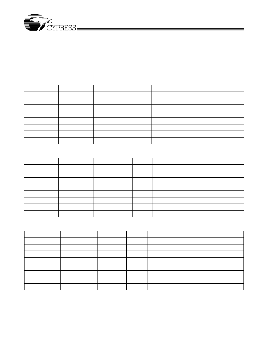
Table 1. Frequency Selections
FS4 FS3 FS2 FS1 FS0
CPU
SDRAM
3V66
PCI
APIC
SS
0
0
0
0
0
75.3
113.0
75.3
37.6
18.8
OFF
0
0
0
0
1
95.0
95.0
63.3
31.6
15.8
≠0.6%
0
0
0
1
0
129.0
129.0
86.0
43.0
21.5
OFF
0
0
0
1
1
150.0
113.0
75.3
37.6
18.8
OFF
0
0
1
0
0
150.0
150.0
75.0
37.5
18.7
OFF
0
0
1
0
1
110.0
110.0
73.0
36.6
18.3
OFF
0
0
1
1
0
140.0
140.0
70.0
35.0
17.5
OFF
0
0
1
1
1
144.0
108.0
72.0
36.0
18.0
OFF
0
1
0
0
0
68.3
102.5
68.3
34.1
17.0
OFF
0
1
0
0
1
105.0
105.0
70.0
35.0
17.5
OFF
0
1
0
1
0
138.0
138.0
69.0
34.5
17.0
OFF
0
1
0
1
1
140.0
105.0
70.0
35.0
17.5
OFF
0
1
1
0
0
66.8
100.2
66.8
33.4
16.7
±0.45%
0
1
1
0
1
100.2
100.2
66.8
33.4
16.7
±0.45%
0
1
1
1
0
133.6
133.6
66.8
33.4
16.7
±0.45%
0
1
1
1
1
133.6
100.2
66.8
33.4
16.7
±0.45%
1
0
0
0
0
157.3
118.0
78.6
39.3
19.6
OFF
1
0
0
0
1
160.0
120.0
80.0
40.0
20.0
OFF
1
0
0
1
0
146.6
110.0
73.3
36.6
18.3
OFF
1
0
0
1
1
122.0
91.5
61.0
30.5
15.2
≠0.6%
1
0
1
0
0
127.0
127.0
84.6
42.3
21.1
OFF
1
0
1
0
1
122.0
122.0
81.3
40.6
20.3
≠0.6%
1
0
1
1
0
117.0
117.0
78.0
39.0
19.5
OFF
1
0
1
1
1
114.0
114.0
76.0
38.0
19.0
OFF
1
1
0
0
0
80.0
120.0
80.0
40.0
20.0
OFF
1
1
0
0
1
78.0
117.0
78.0
39.0
19.5
OFF
1
1
0
1
0
166.0
124.5
83.0
41.5
20.7
OFF
1
1
0
1
1
133.6
133.6
89.0
44.5
22.2
OFF
1
1
1
0
0
66.6
100.0
66.6
33.3
16.6
≠0.6%
1
1
1
0
1
100.0
100.0
66.6
33.3
16.6
≠0.6%
1
1
1
1
0
133.3
133.3
66.6
33.3
16.6
≠0.6%
1
1
1
1
1
133.3
100.0
66.6
33.3
16.6
≠0.6%
Block Diagram
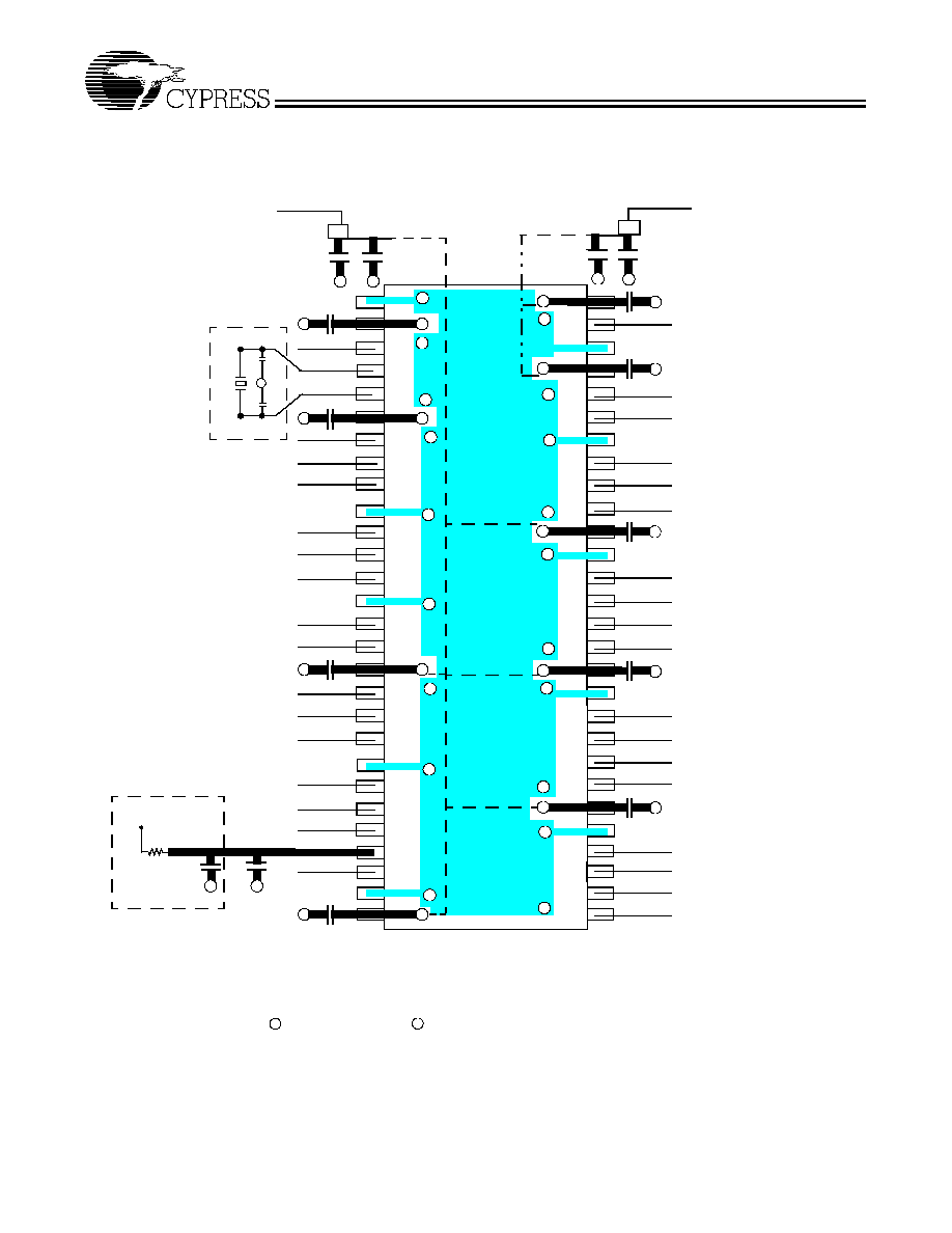
Pin Configuration
Note:
1.
Internal pull-down or pull-up resistors present on inputs marked with
* or ^, respectively. Design should not rely solely on internal pull-up
or pull-down resistor to set I/O pins HIGH or LOW, respectively.
[1]
VDDQ3
VDDQ2
PCI1/FS1*
XTAL
PLL REF FREQ
PLL 1
X2
X1
REF2X/FS3*
PCI3:7
48MHz_1/FS4*
SI0/24_48 MHz#*
PLL2
OSC
VDDQ3
I
2
C
SDATA
Logic
SCLK
3V66_0:2
CPU0:1
APIC
Divider,
Delay,
and
Phase
Control
Logic
3
VDDQ3
2
SDRAM0:12
13
PWRDWN#
PCI0/FS0*
PCI2/FS2*
/2
(FS0:4*)
5
48MHz_0
GND
VDDQ3
REF2X/FS3*
X1
X2
VDDQ3
3V66_0
3V66_1
3V66_2
GND
PCI0/FS0*
PCI1/FS1*
PCI2/FS2*
GND
PCI3
PCI4
VDDQ3
PCI5
PCI6
PCI7
GND
48MHz_0
48MHz_1/FS4*
SIO/24_48MHz#*
W
2
29B
VDDQ2
APIC
GND
VDDQ2
CPU0
CPU1
GND
SDRAM0
SDRAM1
SDRAM2
VDDQ3
GND
SDRAM3
SDRAM4
SDRAM5
SDRAM6
VDDQ3
GND
SDRAM7
SDRAM8
SDRAM9
SDRAM10
VDDQ3
GND
56
55
54
53
52
51
50
49
48
47
46
45
44
43
42
41
40
39
38
37
36
35
34
33
1
2
3
4
5
6
7
8
9
10
11
12
13
14
15
16
17
18
19
20
21
22
23
24
25
26
27
28
32
31
30
29
VDDQ3
SDATA
GND
VDD3
SDRAM11
SDRAM12
PWRDWN#
^
SCLK

W229B
2
I
Pin Definitions
Pin Name
Pin No.
Pin
Type
Pin Description
REF2x/FS3*
3
I/O
Reference Clock with 2x Drive/Frequency Select 3: 3.3V 14.318-MHz clock out-
put. This pin also serves as the select strap to determine device operating frequency
as described in Table 1.
X1
4
I
Crystal Input: This pin has dual functions. It can be used as an external 14.318-
MHz crystal connection or as an external reference frequency input.
X2
5
I
Crystal Output: An input connection for an external 14.318-MHz crystal connec-
tion. If using an external reference, this pin must be left unconnected.
PCI0/FS0*
11
I/O
PCI Clock 0/Frequency Selection 0: 3.3V 33-MHz PCI clock outputs. This pin also
serves as the select strap to determine device operating frequency as described in
Table 1.
PCI1/FS1*
12
I/O
PCI Clock 1/Frequency Selection 1: 3.3V 33-MHz PCI clock outputs. This pin also
serves as the select strap to determine device operating frequency as described in
Table 1.
PCI2/FS2*
13
I/O
PCI Clock 2/Frequency Selection 2: 3.3V 33-MHz PCI clock outputs. This pin also
serves as the select strap to determine device operating frequency as described in
Table 1.
PCI3:7
15, 16, 18, 19,
20
O
PCI Clock 3 through 7: 3.3V 33-MHz PCI clock outputs. PCI0:7 can be individually
turned off via SMBus interface.
3V66_0:2
7, 8, 9
O
66-MHz Clock Output: 3.3V output clocks. The operating frequency is controlled
by FS0:4 (see Table 1).
48MHz_0
22
O
48-MHz Clock Output: 3.3V fixed 48-MHz, non-spread spectrum clock output.
48MHz_1/
FS4*
23
I/O
48-MHz Clock Output/Frequency Selection 4: 3.3V fixed 48-MHz, non-spread
spectrum clock output. This pin also serves as the select strap to determine device
operating frequency as described in Table 1.
SIO/
24_48MHz#*
24
I/O
Clock Output for Super I/O: This is the input clock for a Super I/O (SIO) device.
During power up, it also serves as a selection strap. If it is sampled HIGH, the output
frequency for SIO is 24 MHz. If the input is sampled LOW, the output is 48 MHz.
PWRDWN#
30
I
Power Down Control: LVTTL-compatible input that places the device in power-
down mode when held LOW.
CPU0:1
52, 51
O
CPU Clock Outputs: Clock outputs for the host bus interface. Output frequencies
depending on the configuration of FS0:4. Voltage swing is set by VDDQ2.
SDRAM0:12,
49, 48, 47, 44,
43, 42, 41, 38,
37, 36, 35, 32,
31
O
SDRAM Clock Outputs: 3.3V outputs for SDRAM and chipset. The operating fre-
quency is controlled by FS0:4 (see Table 1).
APIC
55
O
Synchronous APIC Clock Outputs: Clock outputs running synchronous with the
PCI clock outputs. Voltage swing set by VDDQ2.
SDATA
26
I/O
Data pin for SMBus circuitry.
SCLK
29
I
Clock pin for SMBus circuitry.
VDDQ3
2, 6, 17, 25, 34,
40, 46
P
3.3V Power Connection: Power supply for SDRAM output buffers, PCI output buff-
ers, reference output buffers and 48-MHz output buffers. Connect to 3.3V.
VDD3
28
P
3.3V Power Connection: Power supply for PLL core.
VDDQ2
53, 56
P
2.5V Power Connection: Power supply for IOAPIC and CPU output buffers. Con-
nect to 2.5V or 3.3V.
GND
1, 10, 14, 21, 27,
33, 39, 45, 50,
54
G
Ground Connections: Connect all ground pins to the common system ground
plane.
W229B
3
Overview
The W229B is a highly integrated frequency timing generator,
supplying all the required clock sources for an IntelÆ architec-
ture platform using graphics integrated core logic.
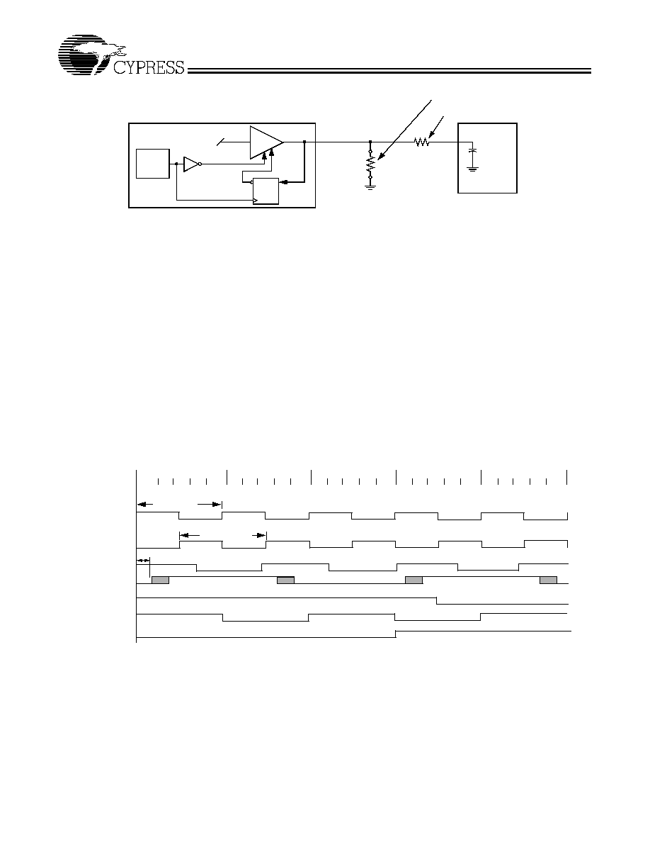
Functional Description
I/O Pin Operation
Pin # 3, 11, 12, 13, 23, and 24 are dual-purpose l/O pins. Upon
power-up the pin acts as a logic input. An external 10-k
strap-
ping resistor should be used. Figure 1 shows a suggested
method for strapping resistor connections.
After 2 ms, the pin becomes an output. Assuming the power
supply has stabilized by then, the specified output frequency
is delivered on the pins. If the power supply has not yet
reached full value, output frequency initially may be below tar-
get but will increase to target once supply voltage has stabi-
lized. In either case, a short output clock cycle may be pro-
duced from the CPU clock outputs when the outputs are
enabled.
Offsets Among Clock Signal Groups
Figure 2, Figure 3, and Figure 4 represent the phase relation-
ship among the different groups of clock outputs from W229B
when it is providing a 66-MHz CPU clock, a 100-MHz CPU
clock, and a 133-MHz CPU clock, respectively. It should be
noted that when CPU clock is operating at 100 MHz, CPU
clock output is 180 degrees out of phase with SDRAM clock
outputs.
Power Down Control
W229B provides one PWRDWN# signal to place the device in
low-power mode. In low-power mode, the PLLs are turned off
and all clock outputs are driven LOW.
Power-on
Reset
Timer
Output Three-state
Data
Latch
Hold
Q
D
W229B
Clock Load
Output
Buffer
10 k
Output
Low
Output Strapping Resistor
Series Termination Resistor
Figure 1. Input Logic Selection Through Resistor Load Option.
CPU 66-MHz
SDRAM 100-MHz
3V66 66-MHz
PCI 33-MHz
REF 14.318-MHz
USB 48-MHz
APIC
0 ns
Figure 2. Group Offset Waveforms (66-MHz CPU Clock, 100-MHz SDRAM Clock).
40 ns
30 ns
20 ns
10 ns
SDRAM 100 Period
CPU 100 Period
Hub-PC
W229B
4
CPU 100-MHz
SDRAM 100-MHz
3V66 66-MHz
PCI 33-MHz
REF 14.318-MHz
USB 48-MHz
APIC
0 ns
Figure 3. Group Offset Waveforms (100-MHz CPU Clock/100-MHz SDRAM Clock).
40 ns
30 ns
20 ns
10 ns
SDRAM 100 Period
CPU 100 Period
Hub-PC
CPU 133-MHz
SDRAM 100-MHz
3V66 66-MHz
PCI 33-MHz
REF 14.318-MHz
USB 48-MHz
DOT 48-MHz
Cycle Repeats
APIC 33-MHz
Figure 4. Group Offset Waveforms (133-MHz CPU/100-MHz SDRAM).
0 ns
40 ns
30 ns
20 ns
10 ns

W229B
5
Notes:
2.
Once the PWRDWN# signal is sampled LOW for two consecutive rising edges of CPU, clocks of interest will be held LOW on the next HIGH-to-LOW transition.
3.
PWRDWN# is an asynchronous input and metastable conditions could exist. This signal is synchronized inside W229B.
4.
The shaded sections on the SDRAM, REF, and USB clocks indicate "Don't Care" states.
5.
Diagrams shown with respect to 100 MHz. Similar operation when CPU is 66 MHz.
CPU 100-MHz
SDRAM 133-MHz
3V66 66-MHz
PCI 33-MHz
REF 14.318-MHz
USB 48-MHz
DOT 48-MHz
APIC 33-MHz
Cycle Repeat
Figure 5. Group Offset Waveform (133-MHz CPU/133-MHz SDRAM).
0 ns
40 ns
30 ns
20 ns
10 ns
1
2
Center
0 n s
2 5 n s
5 0 n s
7 5 n s
VCO Internal
C P U 1 0 0 M H z
3 V 6 6 6 6 M H z
P C I 3 3 M H z
A P I C 3 3 M H z
P w r D w n
S D R A M 1 0 0 M H z
R E F 1 4 . 3 1 8 M H z
U S B 4 8 M H z
Figure 6. W229B PWRDWN# Timing Diagram
[2, 3, 4, 5]
.
W229B
6
Table 2. W229B Maximum Allowed Current
W229B
Condition
Max 2.5V supply consumption
Max discrete cap loads,
VDDQ2 = 2.625V
All static inputs = VDDQ3 or VSS
Max 3.3V supply consumption
Max discrete cap loads
VDDQ3 = 3.465V
All static inputs = VDDQ3 or VSS
Full Active 66 MHz
FSEL4:0 = 01100 (PWRDWN# =1)
70 mA
280 mA
Full Active 100 MHz
FSEL4:0 = 11101 (PWRDWN# = 1)
100 mA
280 mA
Full Active 133 MHz
FSEL4:0 = 11110 (PWRDWN# = 1)
50 mA
400 mA
W229B
7
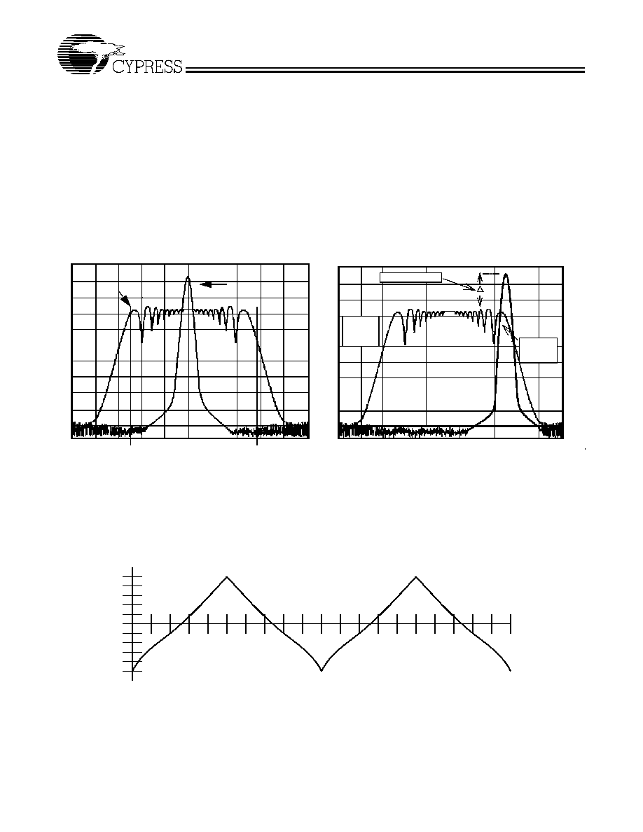
Spread Spectrum Frequency Timing Generator
The device generates a clock that is frequency modulated in
order to increase the bandwidth that it occupies. By increasing
the bandwidth of the fundamental and its harmonics, the am-
plitudes of the radiated electromagnetic emissions are re-
duced. This effect is depicted in Figure 7.
As shown in Figure 7, a harmonic of a modulated clock has a
much lower amplitude than that of an unmodulated signal. The
reduction in amplitude is dependent on the harmonic number
and the frequency deviation or spread. The equation for the
reduction is
dB = 6.5 + 9*log
10
(P) + 9*log
10
(F)
Where P is the percentage of deviation and F is the frequency
in MHz where the reduction is measured.
The output clock is modulated with a waveform depicted in
Figure 8. This waveform, as discussed in "Spread Spectrum
Clock Generation for the Reduction of Radiated Emissions" by
Bush, Fessler, and Hardin, produces the maximum reduction
in the amplitude of radiated electromagnetic emissions. The
deviation selected for this chip is ±0.45% or -0.6% of the se-
lected frequency. Figure 7 details the Cypress spreading pat-
tern. Cypress does offer options with more spread and greater
EMI reduction. Contact your local Sales representative for de-
tails on these devices.
SSFTG
Typical Clock
Frequency Span (MHz)
Center Spread
A
m
pli
t
ude
(
d
B
)
Spread
Spectrum
Enabled
EMI Reduction
Spread
Spectrum
Non-
Frequency Span (MHz)
Down Spread
A
m
pl
i
t
ud
e
(dB
)
Figure 7. Clock Harmonic with and without SSCG Modulation Frequency Domain Representa-
tion.
MAX.
MIN.
10
%
20
%
30
%
40
%
50
%
60
%
70
%
80
%
90
%
10
0%
10
%
20
%
30
%
40
%
50
%
60
%
70
%
80
%
90
%
10
0%
F
R
EQ
UENC
Y
Figure 8. Typical Modulation Profile.

W229B
8
Serial Data Interface
The W229B features a two-pin, serial data interface that can
be used to configure internal register settings that control par-
ticular device functions.
Data Protocol
The clock driver serial protocol accepts only block writes from
the controller. The bytes must be accessed in sequential order
from lowest to highest byte with the ability to stop after any
complete byte has been transferred. Indexed bytes are not al-
lowed.
A block write begins with a slave address and a write condition.
After the command code the core logic issues a byte count
which describes how many more bytes will follow in the mes-
sage. If the host had 20 bytes to send, the first byte would be
the number 20 (14h), followed by the 20 bytes of data. The byte
count may not be 0. A block write command is allowed to trans-
fer a maximum of 32 data bytes. The slave receiver address
for W229B is 11010010. Figure 9 shows an example of a block
write.
The command code and the byte count bytes are required as
the first two bytes of any transfer. W229B expects a command
code of 0000 0000. The byte count byte is the number of ad-
ditional bytes required for the transfer, not counting the com-
mand code and byte count bytes. Additionally, the byte count
byte is required to be a minimum of 1 byte and a maximum of
32 bytes to satisfy the above requirement. Table 3 shows an
example of a possible byte count value.
A transfer is considered valid after the acknowledge bit corre-
sponding to the byte count is read by the controller. The com-
mand code and byte count bytes are ignored by the W229B.
However, these bytes must be included in the data write se-
quence to maintain proper byte allocation.
Notes:
6.
The acknowledgment bit is returned by the slave/receiver (W229B).
7.
Bytes 6 and 7 are not defined for W229B.
1 bit
7 bits
1
1
8 bits
1
Start bit
Slave Address
R/W
Ack
Command Code
Ack
Byte Count = N
Ack
Data Byte 1
Ack
Data Byte 2
Ack
...
Data Byte N
Ack
Stop
1 bit
8 bits
1
8 bits
1
8 bits
1
1
Figure 9. An Example of a Block Write
[6]
.
Table 3. Example of Possible Byte Count Value
Byte Count Byte
Notes
MSB
LSB
0000
0000
Not allowed. Must have at least one byte.
0000
0001
Data for functional and frequency select register (currently byte 0 in spec)
0000
0010
Reads first two bytes of data. (byte 0 then byte 1)
0000
0011
Reads first three bytes (byte 0, 1, 2 in order)
0000
0100
Reads first four bytes (byte 0, 1, 2, 3 in order)
0000
0101
Reads first five bytes (byte 0, 1, 2, 3, 4 in order)
[7]
0000
0110
Reads first six bytes (byte 0, 1, 2, 3, 4, 5 in order)
[7]
0000
0111
Reads first seven bytes (byte 0, 1, 2, 3, 4, 5, 6 in order)
0010
0000
Max. byte count supported = 32
Table 4. Serial Data Interface Control Functions Summary
Control Function
Description
Common Application
Output Disable
Any individual clock output(s) can be disabled.
Disabled outputs are actively held LOW.
Unused outputs are disabled to reduce EMI and sys-
tem power. Examples are clock outputs to unused
PCI slots.
(Reserved)
Reserved function for future device revision or pro-
duction device testing.
No user application. Register bit must be written as 0.
W229B
9
W229B Serial Configuration Map
1. The serial bits will be read by the clock driver in the following
order:
Byte 0 - Bits 7, 6, 5, 4, 3, 2, 1, 0
Byte 1 - Bits 7, 6, 5, 4, 3, 2, 1, 0
Byte N - Bits 7, 6, 5, 4, 3, 2, 1, 0
2. All unused register bits (reserved and N/A) should be writ-
ten to a "0" level.
3. All register bits labeled "Initialize to 0" must be written to
zero during initialization. Failure to do so may result in high-
er than normal operating current. The controller will read
back the written value.
Note:
8.
Inactive means outputs are held LOW and are disabled from switching. These outputs are designed to be configured at power-on and are not expected to be
configured during the normal modes of operation.
Byte 0: Control Register (1 = Enable, 0 = Disable)
[8]
Bit
Pin#
Name
Default
Pin Function
Bit 7
-
Reserved
0
Reserved
Bit 6
-
Reserved
0
Reserved
Bit 5
-
Reserved
0
Reserved
Bit 4
-
Reserved
0
Reserved
Bit 3
-
Reserved
0
Reserved
Bit 2
24
SIO/24_48 MHz
1
(Active/Inactive)
Bit 1
22, 23
48 MHz
1
(Active/Inactive)
Bit 0
-
Reserved
0
Reserved
Byte 1: Control Register (1 = Enable, 0 = Disable)
[8]
Bit
Pin#
Name
Default
Pin Description
Bit 7
38
SDRAM7
1
(Active/Inactive)
Bit 6
41
SDRAM6
1
(Active/Inactive)
Bit 5
42
SDRAM5
1
(Active/Inactive)
Bit 4
43
SDRAM4
1
(Active/Inactive)
Bit 3
44
SDRAM3
1
(Active/Inactive)
Bit 2
47
SDRAM2
1
(Active/Inactive)
Bit 1
48
SDRAM1
1
(Active/Inactive)
Bit 0
49
SDRAM0
1
(Active/Inactive)
Byte 2: Control Register (1 = Enable, 0 = Disable)
[8]
Bit
Pin#
Name
Default
Pin Description
Bit 7
20
PCI7
1
(Active/Inactive)
Bit 6
19
PCI6
1
(Active/Inactive)
Bit 5
18
PCI5
1
(Active/Inactive)
Bit 4
16
PCI4
1
(Active/Inactive)
Bit 3
15
PCI3
1
(Active/Inactive)
Bit 2
13
PCI2
1
(Active/Inactive)
Bit 1
12
PCI1
1
(Active/Inactive)
Bit 0
11
PCI0
1
(Active/Inactive)

W229B
10
Byte 3: Reserved Register (1 = Enable, 0 = Disable)
Bit
Pin#
Name
Default
Pin Description
Bit 7
-
Reserved
0
Reserved
Bit 6
-
Reserved
0
Reserved
Bit 5
-
Reserved
0
Reserved
Bit 4
-
Reserved
0
Reserved
Bit 3
55
APIC
1
(Active/Inactive)
Bit 2
-
Reserved
0
Reserved
Bit 1
-
Reserved
0
Reserved
Bit 0
-
Reserved
0
Reserved
Byte 4: Reserved Register (1 = Enable, 0 = Disable)
Bit
Pin#
Name
Default
Pin Function
Bit 7
-
SEL3
0
See Table 5
Bit 6
-
SEL2
0
See Table 5
Bit 5
-
SEL1
0
See Table 5
Bit 4
-
SEL0
0
See Table 5
Bit 3
-
FS(0:4) Override
0
0 = Select operating frequency by FS(0:4) strapping
1 = Select operating frequency by SEL(0:4) bit settings
Bit 2
-
SEL4
0
See Table 5
Bit 1
-
Reserved
0
Reserved
Bit 0
-
Test Mode
0
0 = Normal
1 = Three-stated
Byte 5: Reserved Register (1 = Enable, 0 = Disable)
Bit
Pin#
Name
Default
Pin Description
Bit 7
9
3V66_2
1
(Active/Inactive)
Bit 6
8
3V66_1
1
(Active/Inactive)
Bit 5
7
3V66_0
1
(Active/Inactive)
Bit 4
31
SDRAM12
1
(Active/Inactive)
Bit 3
32
SDRAM11
1
(Active/Inactive)
Bit 2
35
SDRAM10
1
(Active/Inactive)
Bit 1
36
SDRAM9
1
(Active/Inactive)
Bit 0
37
SDRAM8
1
(Active/Inactive)
Byte 6: Reserved Register (1 = Enable, 0 = Disable)
Bit
Pin#
Name
Default
Pin Description
Bit 7
-
Reserved
0
Reserved
Bit 6
-
Reserved
0
Reserved
Bit 5
-
Reserved
0
Reserved
Bit 4
-
Reserved
0
Reserved
Bit 3
-
Reserved
0
Reserved
Bit 2
-
Reserved
0
Reserved
Bit 1
-
Reserved
0
Reserved

W229B
11
Bit 0
-
Reserved
0
Reserved
Table 5. Additional Frequency Selections through Serial Data Interface Data Bytes
Input Conditions
Output Frequency
Data Byte 4, Bit 3 = 1
CPU
SDRAM
3V66
PCI
APIC
Spread
Spectrum
Bit 2
SEL_4
Bit 7
SEL_3
Bit 6
SEL_2
Bit 5
SEL_1
Bit 4
SEL_0
0
0
0
0
0
75.3
113.0
75.3
37.6
18.8
OFF
0
0
0
0
1
95.0
95.0
63.3
31.6
15.8
≠0.6%
0
0
0
1
0
129.0
129.0
86.0
43.0
21.5
OFF
0
0
0
1
1
150.0
113.0
75.3
37.6
18.8
OFF
0
0
1
0
0
150.0
150.0
75.0
37.5
18.7
OFF
0
0
1
0
1
110.0
110.0
73.0
36.6
18.3
OFF
0
0
1
1
0
140.0
140.0
70.0
35.0
17.5
OFF
0
0
1
1
1
144.0
108.0
72.0
36.0
18.0
OFF
0
1
0
0
0
68.3
102.5
68.3
34.1
17.0
OFF
0
1
0
0
1
105.0
105.0
70.0
35.0
17.5
OFF
0
1
0
1
0
138.0
138.0
69.0
34.5
17.0
OFF
0
1
0
1
1
140.0
105.0
70.0
35.0
17.5
OFF
0
1
1
0
0
66.8
100.2
66.8
33.4
16.7
±0.45%
0
1
1
0
1
100.2
100.2
66.8
33.4
16.7
±0.45%
0
1
1
1
0
133.6
133.6
66.8
33.4
16.7
±0.45%
0
1
1
1
1
133.6
100.2
66.8
33.4
16.7
±0.45%
1
0
0
0
0
157.3
118.0
78.6
39.3
19.6
OFF
1
0
0
0
1
160.0
120.0
80.0
40.0
20.0
OFF
1
0
0
1
0
146.6
110.0
73.3
36.6
18.3
OFF
1
0
0
1
1
122.0
91.5
61.0
30.5
15.2
≠0.6%
1
0
1
0
0
127.0
127.0
84.6
42.3
21.1
OFF
1
0
1
0
1
122.0
122.0
81.3
40.6
20.3
≠0.6%
1
0
1
1
0
117.0
117.0
78.0
39.0
19.5
OFF
1
0
1
1
1
114.0
114.0
76.0
38.0
19.0
OFF
1
1
0
0
0
80.0
120.0
80.0
40.0
20.0
OFF
1
1
0
0
1
78.0
117.0
78.0
39.0
19.5
OFF
1
1
0
1
0
166.0
124.5
83.0
41.5
20.7
OFF
1
1
0
1
1
133.6
133.6
89.0
44.5
22.2
OFF
1
1
1
0
0
66.6
100.0
66.6
33.3
16.6
≠0.6%
1
1
1
0
1
100.0
100.0
66.6
33.3
16.6
≠0.6%
1
1
1
1
0
133.3
133.3
66.6
33.3
16.6
≠0.6%
1
1
1
1
1
133.3
100.0
66.6
33.3
16.6
≠0.6%
Byte 6: Reserved Register (1 = Enable, 0 = Disable)
Bit
Pin#
Name
Default
Pin Description
W229B
12
DC Electrical Characteristics
DC parameters must be sustainable under steady state (DC) conditions.
Note:
9.
Input Leakage Current does not include inputs with pull-up or pull-down resistors.
Absolute Maximum DC Power Supply
Parameter
Description
Min.
Max.
Unit
V
DDQ3
3.3V Core Supply Voltage
≠0.5
4.6
V
V
DDQ2
2.5V I/O Supply Voltage
≠0.5
3.6
V
T
S
Storage Temperature
≠65
150
∞C
Absolute Maximum DC I/O
Parameter
Description
Min.
Max.
Unit
V
i/o3
3.3V Core Supply Voltage
≠0.5
4.6
V
V
i/o3
2.5V I/O Supply Voltage
≠0.5
3.6
V
ESD prot.
Input ESD Protection
2000
V
DC Operating Requirements
Parameter
Description
Condition
Min.
Max.
Unit
V
DD3
3.3V Core Supply Voltage
3.3V±5%
3.135
3.465
V
V
DDQ3
3.3V I/O Supply Voltage
3.3V±5%
3.135
3.465
V
V
DDQ2
2.5V I/O Supply Voltage
2.5V±5%
2.375
2.625
V
V
DD3
=
3.3V±5%
V
ih3
3.3V Input High Voltage
V
DD3
2.0
V
DD
+ 0.3
V
V
il3
3.3V Input Low Voltage
V
SS
≠ 0.3
0.8
V
I
il
Input Leakage Current
[9]
0<V
in
<V
DD3
≠5
+5
µ
A
V
DDQ2
=
2.5V±5%
V
oh2
2.5V Output High Voltage
I
oh
=(≠1 mA)
2.0
V
V
ol2
2.5V Output Low Voltage
I
ol
=(1 mA)
0.4
V
V
DDQ3
=
3.3V±5%
V
oh3
3.3V Output High Voltage
I
oh
=(≠1 mA)
2.4
V
V
ol3
3.3V Output Low Voltage
I
ol
=(1 mA)
0.4
V
V
DDQ3
=
3.3V±5%
V
poh3
PCI Bus Output High Voltage
I
oh
=(≠1 mA)
2.4
V
V
pol3
PCI Bus Output Low Voltage
I
ol
=(1 mA)
0.55
V
C
in
Input Pin Capacitance
5
pF
C
xtal
Xtal Pin Capacitance
13.5
22.5
pF
C
out
Output Pin Capacitance
6
pF
L
pin
Pin Inductance
0
7
nH
T
a
Ambient Temperature
No Airflow
0
70
∞C
W229B
13
AC Electrical Characteristics
T
A
= 0∞C to +70∞C, V
DDQ3
= 3.3V±5%, V
DDQ2
= 2.5V±5%
f
XTL
= 14.31818 MHz
Notes:
10. Period, jitter, offset, and skew measured on rising edge at 1.25 for 2.5V clocks and at 1.5V for 3.3V clocks.
11. T
HIGH
is measured at 2.0V for 2.5V outputs, 2.4V for 3.3V outputs.
12. T
LOW
is measured at 0.4V for all outputs.
13. The time specified is measured from when V
DDQ3
achieves its nominal operating level (typical condition V
DDQ3
= 3.3V) until the frequency output is stable and
operating within specification.
14. T
RISE
and T
FALL
are measured as a transition through the threshold region V
ol
= 0.4V and V
oh
= 2.0V (1 mA) JEDEC specification for 2.5V outputs, and
V
ol
= 0.4V and V
oh
= 2.4V for 3.3V outputs.
Parameter
Description
66.6-MHz Host
100-MHz Host
133-MHz Host
Unit
Notes
Min.
Max.
Min.
Max.
Min.
Max.
T
Period
Host/CPUCLK Period
15.0
15.5
10.0
10.5
7.5
8.0
ns
10
T
HIGH
Host/CPUCLK High Time
5.2
N/A
3.0
N/A
1.87
N/A
ns
13
T
LOW
Host/CPUCLK Low Time
5.0
N/A
2.8
N/A
1.67
N/A
ns
T
RISE
Host/CPUCLK Rise Time
0.4
1.6
0.4
1.6
0.4
1.6
ns
14
T
FALL
Host/CPUCLK Fall Time
0.4
1.6
0.4
1.6
0.4
1.6
ns
14
T
Period
SDRAM CLK Period
10.0
10.5
10.0
10.5
10.0
10.5
ns
10
T
HIGH
SDRAM CLK High Time
3.0
N/A
3.0
N/A
3.0
N/A
ns
13
T
LOW
SDRAM CLK Low Time
2.8
N/A
2.8
N/A
2.8
N/A
ns
T
RISE
SDRAM CLK Rise Time
0.4
1.6
0.4
1.6
0.4
1.6
ns
14
T
FALL
SDRAM CLK Fall Time
0.4
1.6
0.4
1.6
0.4
1.6
ns
14
T
Period
APIC 33-MHz CLK Period
30.0
N/A
30.0
N/A
30.0
N/A
ns
10
T
HIGH
APIC 33-MHz CLK High Time
12.0
N/A
12.0
N/A
12.0
N/A
ns
13
T
LOW
APIC 33-MHz CLK Low Time
12.0
N/A
12.0
N/A
12.0
N/A
ns
T
RISE
APIC CLK Rise Time
0.4
1.6
0.4
1.6
0.4
1.6
ns
14
T
FALL
APIC CLK Fall Time
0.4
1.6
0.4
1.6
0.4
1.6
ns
14
T
Period
3V66 CLK Period
15.0
16.0
15.0
16.0
15.0
16.0
ns
10, 12
T
HIGH
3V66 CLK High Time
5.25
N/A
5.25
N/A
5.25
N/A
ns
13
T
LOW
3V66 CLK Low Time
5.05
N/A
5.05
N/A
5.05
N/A
ns
T
RISE
3V66 CLK Rise Time
0.5
2.0
0.5
2.0
0.5
2.0
ns
14
T
FALL
3V66 CLK Fall Time
0.5
2.0
0.5
2.0
0.5
2.0
ns
14
T
Period
PCI CLK Period
30.0
N/A
30.0
N/A
30.0
N/A
ns
10, 11
T
HIGH
PCI CLK High Time
12.0
N/A
12.0
N/A
12.0
N/A
ns
13
T
LOW
PCI CLK Low Time
12.0
N/A
12.0
N/A
12.0
N/A
ns
T
RISE
PCI CLK Rise Time
0.5
2.0
0.5
2.0
0.5
2.0
ns
14
T
FALL
PCI CLK Fall Time
0.5
2.0
0.5
2.0
0.5
2.0
ns
14
tp
ZL
, tp
ZH
Output Enable Delay (All outputs)
1.0
10.0
1.0
10.0
1.0
10.0
ns
tp
LZ
, tp
ZH
Output Disable Delay
(All outputs)
1.0
10.0
1.0
10.0
1.0
10.0
ns
t
stable
All Clock Stabilization from
Power-Up
3
3
3
ms
W229B
14
Intel is a registered trademark of Intel Corporation.
Document #: 38-00889-*C
Group Skew and Jitter Limits
Output Group
Pin-Pin Skew Max.
Cycle-Cycle Jitter
Duty Cycle
Nom V
DD
Skew, Jitter
Measure Point
CPU
175 ps
250 ps
45/55
2.5V
1.25V
SDRAM
250 ps
250 ps
45/55
3.3V
1.5V
APIC
250 ps
500 ps
45/55
2.5V
1.25V
48MHz
250 ps
500 ps
45/55
3.3V
1.5V
3V66
175 ps
500 ps
45/55
3.3V
1.5V
PCI
500 ps
500 ps
45/55
3.3V
1.5V
REF
N/A
1000 ps
45/55
3.3V
1.5V
Clock Output Wave
2.5V Clocking
3.3V Clocking
Test Point
Test Load
T
PERIOD
Duty Cycle
T
HIGH
2.0
1.25
0.4
T
LOW
T
RISE
T
FALL
T
LOW
T
RISE
T
FALL
T
PERIOD
Duty Cycle
T
HIGH
2.4
1.5
0.4
Output
Buffer
Interface
Interface
Figure 10. Output Buffer.
Ordering Information
Ordering Code
Package Name
Package Type
W229B
H
56-pin SSOP (300 mils)
W229B
15
Layout Example
56
55
54
53
52
51
50
49
48
47
46
45
44
43
42
6
7
13
19
20
24
G = VIA to GND plane layer V =VIA to respective supply plane layer
Note: 1) Each supply plane or strip should have a ferrite bead and capacitors.
G
+2.5V Supply
1
2
3
4
5
8
9
11
12
14
15
16
17
22
23
21
25
26
27
28
40
39
18
41
10
31
30
29
36
35
34
33
32
37
38
C7
C8
FB
+3.3V Supply
C4
C1 & C3 = 10≠22
µ
F
C2 & C4 = 0.005
µ
F
10
µ
F
FB
C1
C2
FB = Vishay Dale ILB1206 - 300 (300
@ 100 MHz) or TDK ACB2012L120
0.005
µ
F
G
G
G
G
VDDQ2
VDDQ3
C3
C5 = 10
µ
F
C6 = 0.1
µ
F
G
10
VDDQ3
C5
C6
G
V
G
V
G
V
G
V
G
V
G
V
G
V
G
V
G
V
W229B
Core
VDDQ3
G
G
G
G
G
G
G
G
G
G
G
G
G
G
G
G
G
G
G
10
µ
F
0.005
µ
F
*Note 3
R1
*Note 4
2) Bypass capacitors are 0.1
µ
F ceramic unless otherwise stated.
3) C7 and C8 can be used to correct the crystal oscillaotr frequency if the crystal used is specified for more then
4) If an on-board video controler uses 48 MHz then use R1 and C5 to reduce long-term jitter on the 48 MHz clock.
G
VDDQ3, as shown, or to +3.3V supply.
R1 can connect to
18 pF Cload.

W229B
© Cypress Semiconductor Corporation, 2001. The information contained herein is subject to change without notice. Cypress Semiconductor Corporation assumes no responsibility for the use
of any circuitry other than circuitry embodied in a Cypress Semiconductor product. Nor does it convey or imply any license under patent or other rights. Cypress Semiconductor does not authorize
its products for use as critical components in life-support systems where a malfunction or failure may reasonably be expected to result in significant injury to the user. The inclusion of Cypress
Semiconductor products in life-support systems application implies that the manufacturer assumes all risk of such use and in doing so indemnifies Cypress Semiconductor against all charges.
Package Diagram
56-Pin Shrink Small Outline Package (SSOP, 300 mils)