 | –≠–ª–µ–∫—Ç—Ä–æ–Ω–Ω—ã–π –∫–æ–º–ø–æ–Ω–µ–Ω—Ç: W229BH | –°–∫–∞—á–∞—Ç—å:  PDF PDF  ZIP ZIP |

Frequency Generator for Integrated Core Logic
with 133-MHz FSB
W229B
Cypress Semiconductor Corporation
∑
3901 North First Street
∑
San Jose
∑
CA 95134
∑
408-943-2600
Document #: 38-07223 Rev. *A
Revised December 21, 2002
Features
∑ Maximized EMI suppression using Cypress's Spread
Spectrum technology
∑ Low jitter and tightly controlled clock skew
∑ Highly integrated device providing clocks required for
CPU, core logic, and SDRAM
∑ Two copies of CPU clock
∑ Thirteen copies of SDRAM clock
∑ Eight copies of PCI clock
∑ One copy of synchronous APIC clock
∑ Three copies of 66-MHz outputs
∑ Two copies of 48-MHz outputs
∑ One copy of selectable 24- or 48-MHz clock
∑ One copy of double strength 14.31818-MHz reference
clock
∑ Power-down control
∑ SMBus interface for turning off unused clocks
Key Specifications
CPU, SDRAM Outputs Cycle-to-Cycle Jitter: ............. 250 ps
APIC, 48-MHz, 3V66, PCI Outputs
Cycle-to-Cycle Jitter:................................................... 500 ps
CPU, 3V66 Output Skew: ........................................... 175 ps
SDRAM, APIC, 48-MHz Output Skew: ....................... 250 ps
PCI Output Skew: ....................................................... 500 ps
CPU to SDRAM Skew (@ 133 MHz) ....................... ± 0.5 ns
CPU to SDRAM Skew (@ 100 MHz) ................. 4.5 to 5.5 ns
CPU to 3V66 Skew (@ 66 MHz)........................ 7.0 to 8.0 ns
3V66 to PCI Skew (3V66 lead) .......................... 1.5 to 3.5 ns
PCI to APIC Skew..................................................... ± 0.5 ns
Table 1. Frequency Selections
FS4 FS3 FS2 FS1 FS0
CPU
SDRAM
3V66
PCI
APIC
SS
0
0
0
0
0
75.3
113.0
75.3
37.6
18.8
OFF
0
0
0
0
1
95.0
95.0
63.3
31.6
15.8
≠0.6%
0
0
0
1
0
129.0
129.0
86.0
43.0
21.5
OFF
0
0
0
1
1
150.0
113.0
75.3
37.6
18.8
OFF
0
0
1
0
0
150.0
150.0
75.0
37.5
18.7
OFF
0
0
1
0
1
110.0
110.0
73.0
36.6
18.3
OFF
0
0
1
1
0
140.0
140.0
70.0
35.0
17.5
OFF
0
0
1
1
1
144.0
108.0
72.0
36.0
18.0
OFF
0
1
0
0
0
68.3
102.5
68.3
34.1
17.0
OFF
0
1
0
0
1
105.0
105.0
70.0
35.0
17.5
OFF
0
1
0
1
0
138.0
138.0
69.0
34.5
17.0
OFF
0
1
0
1
1
140.0
105.0
70.0
35.0
17.5
OFF
0
1
1
0
0
66.8
100.2
66.8
33.4
16.7
±0.45%
0
1
1
0
1
100.2
100.2
66.8
33.4
16.7
±0.45%
0
1
1
1
0
133.6
133.6
66.8
33.4
16.7
±0.45%
0
1
1
1
1
133.6
100.2
66.8
33.4
16.7
±0.45%
1
0
0
0
0
157.3
118.0
78.6
39.3
19.6
OFF
1
0
0
0
1
160.0
120.0
80.0
40.0
20.0
OFF
1
0
0
1
0
146.6
110.0
73.3
36.6
18.3
OFF
1
0
0
1
1
122.0
91.5
61.0
30.5
15.2
≠0.6%
1
0
1
0
0
127.0
127.0
84.6
42.3
21.1
OFF
1
0
1
0
1
122.0
122.0
81.3
40.6
20.3
≠0.6%
1
0
1
1
0
117.0
117.0
78.0
39.0
19.5
OFF
1
0
1
1
1
114.0
114.0
76.0
38.0
19.0
OFF
1
1
0
0
0
80.0
120.0
80.0
40.0
20.0
OFF
1
1
0
0
1
78.0
117.0
78.0
39.0
19.5
OFF
1
1
0
1
0
166.0
124.5
83.0
41.5
20.7
OFF
1
1
0
1
1
133.6
133.6
89.0
44.5
22.2
OFF
1
1
1
0
0
66.6
100.0
66.6
33.3
16.6
≠0.6%
1
1
1
0
1
100.0
100.0
66.6
33.3
16.6
≠0.6%
1
1
1
1
0
133.3
133.3
66.6
33.3
16.6
≠0.6%
1
1
1
1
1
133.3
100.0
66.6
33.3
16.6
≠0.6%
Block Diagram
Pin Configuration
Note:
1.
Internal pull-down or pull-up resistors present on inputs marked with
* or ^, respectively. Design should not rely solely on internal pull-up
or pull-down resistor to set I/O pins HIGH or LOW, respectively.
[1]
VDDQ3
VDDQ2
PCI1/FS1*
XTAL
PLL REF FREQ
PLL 1
X2
X1
REF2X/FS3*
PCI3:7
48MHz_1/FS4*
SI0/24_48 MHz#*
PLL2
OSC
VDDQ3
I
2
C
SDATA
Logic
SCLK
3V66_0:2
CPU0:1
APIC
Divider,
Delay,
and
Phase
Control
Logic
3
VDDQ3
2
SDRAM0:12
13
PWRDWN#
PCI0/FS0*
PCI2/FS2*
/2
(FS0:4*)
5
48MHz_0
GND
VDDQ3
REF2X/FS3*
X1
X2
VDDQ3
3V66_0
3V66_1
3V66_2
GND
PCI0/FS0*
PCI1/FS1*
PCI2/FS2*
GND
PCI3
PCI4
VDDQ3
PCI5
PCI6
PCI7
GND
48MHz_0
48MHz_1/FS4*
SIO/24_48MHz#*
W
2
29B
VDDQ2
APIC
GND
VDDQ2
CPU0
CPU1
GND
SDRAM0
SDRAM1
SDRAM2
VDDQ3
GND
SDRAM3
SDRAM4
SDRAM5
SDRAM6
VDDQ3
GND
SDRAM7
SDRAM8
SDRAM9
SDRAM10
VDDQ3
GND
56
55
54
53
52
51
50
49
48
47
46
45
44
43
42
41
40
39
38
37
36
35
34
33
1
2
3
4
5
6
7
8
9
10
11
12
13
14
15
16
17
18
19
20
21
22
23
24
25
26
27
28
32
31
30
29
VDDQ3
SDATA
GND
VDD3
SDRAM11
SDRAM12
PWRDWN#
^
SCLK

W229B
Document #: 38-07223 Rev. *A
Page 2 of 17
I
Pin Definitions
Pin Name
Pin No.
Pin
Type
Pin Description
REF2x/FS3*
3
I/O
Reference Clock with 2x Drive/Frequency Select 3: 3.3V 14.318-MHz clock out-
put. This pin also serves as the select strap to determine device operating frequency
as described in Table 1.
X1
4
I
Crystal Input: This pin has dual functions. It can be used as an external 14.318-
MHz crystal connection or as an external reference frequency input.
X2
5
I
Crystal Output: An input connection for an external 14.318-MHz crystal connec-
tion. If using an external reference, this pin must be left unconnected.
PCI0/FS0*
11
I/O
PCI Clock 0/Frequency Selection 0: 3.3V 33-MHz PCI clock outputs. This pin also
serves as the select strap to determine device operating frequency as described in
Table 1.
PCI1/FS1*
12
I/O
PCI Clock 1/Frequency Selection 1: 3.3V 33-MHz PCI clock outputs. This pin also
serves as the select strap to determine device operating frequency as described in
Table 1.
PCI2/FS2*
13
I/O
PCI Clock 2/Frequency Selection 2: 3.3V 33-MHz PCI clock outputs. This pin also
serves as the select strap to determine device operating frequency as described in
Table 1.
PCI3:7
15, 16, 18, 19,
20
O
PCI Clock 3 through 7: 3.3V 33-MHz PCI clock outputs. PCI0:7 can be individually
turned off via SMBus interface.
3V66_0:2
7, 8, 9
O
66-MHz Clock Output: 3.3V output clocks. The operating frequency is controlled
by FS0:4 (see Table 1).
48MHz_0
22
O
48-MHz Clock Output: 3.3V fixed 48-MHz, non-spread spectrum clock output.
48MHz_1/
FS4*
23
I/O
48-MHz Clock Output/Frequency Selection 4: 3.3V fixed 48-MHz, non-spread
spectrum clock output. This pin also serves as the select strap to determine device
operating frequency as described in Table 1.
SIO/
24_48MHz#*
24
I/O
Clock Output for Super I/O: This is the input clock for a Super I/O (SIO) device.
During power up, it also serves as a selection strap. If it is sampled HIGH, the output
frequency for SIO is 24 MHz. If the input is sampled LOW, the output is 48 MHz.
PWRDWN#
30
I
Power Down Control: LVTTL-compatible input that places the device in power-
down mode when held LOW.
CPU0:1
52, 51
O
CPU Clock Outputs: Clock outputs for the host bus interface. Output frequencies
depending on the configuration of FS0:4. Voltage swing is set by VDDQ2.
SDRAM0:12,
49, 48, 47, 44,
43, 42, 41, 38,
37, 36, 35, 32,
31
O
SDRAM Clock Outputs: 3.3V outputs for SDRAM and chipset. The operating fre-
quency is controlled by FS0:4 (see Table 1).
APIC
55
O
Synchronous APIC Clock Outputs: Clock outputs running synchronous with the
PCI clock outputs. Voltage swing set by VDDQ2.
SDATA
26
I/O
Data pin for SMBus circuitry.
SCLK
29
I
Clock pin for SMBus circuitry.
VDDQ3
2, 6, 17, 25, 34,
40, 46
P
3.3V Power Connection: Power supply for SDRAM output buffers, PCI output buff-
ers, reference output buffers and 48-MHz output buffers. Connect to 3.3V.
VDD3
28
P
3.3V Power Connection: Power supply for PLL core.
VDDQ2
53, 56
P
2.5V Power Connection: Power supply for IOAPIC and CPU output buffers. Con-
nect to 2.5V or 3.3V.
GND
1, 10, 14, 21, 27,
33, 39, 45, 50,
54
G
Ground Connections: Connect all ground pins to the common system ground
plane.

W229B
Document #: 38-07223 Rev. *A
Page 3 of 17
Overview
The W229B is a highly integrated frequency timing generator,
supplying all the required clock sources for an IntelÆ architec-
ture platform using graphics integrated core logic.
Functional Description
I/O Pin Operation
Pin # 3, 11, 12, 13, 23, and 24 are dual-purpose l/O pins. Upon
power-up the pin acts as a logic input. An external 10-k
strap-
ping resistor should be used. Figure 1 shows a suggested
method for strapping resistor connections.
After 2 ms, the pin becomes an output. Assuming the power
supply has stabilized by then, the specified output frequency
is delivered on the pins. If the power supply has not yet
reached full value, output frequency initially may be below tar-
get but will increase to target once supply voltage has stabi-
lized. In either case, a short output clock cycle may be pro-
duced from the CPU clock outputs when the outputs are
enabled.
Offsets Among Clock Signal Groups
Figure 2, Figure 3, and Figure 4 represent the phase relation-
ship among the different groups of clock outputs from W229B
when it is providing a 66-MHz CPU clock, a 100-MHz CPU
clock, and a 133-MHz CPU clock, respectively. It should be
noted that when CPU clock is operating at 100 MHz, CPU
clock output is 180 degrees out of phase with SDRAM clock
outputs.
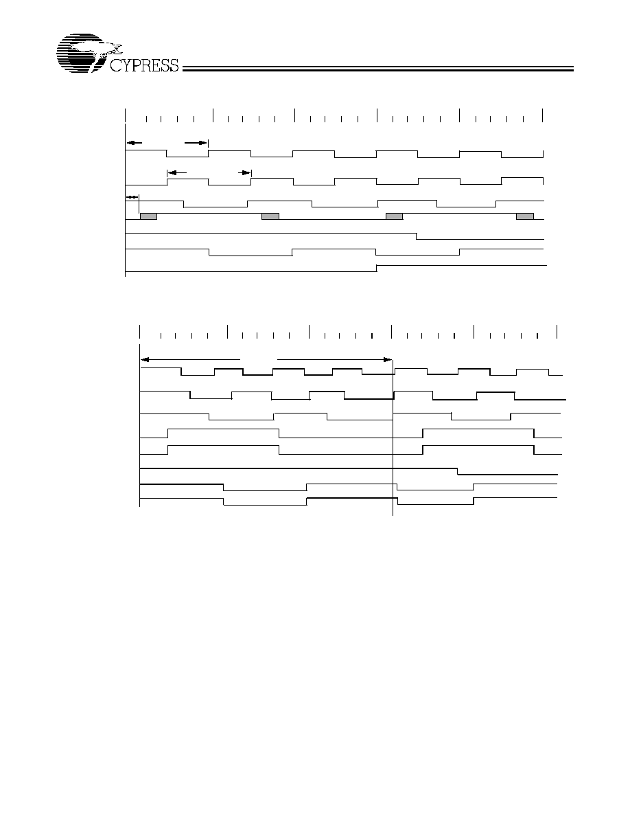
Power Down Control
W229B provides one PWRDWN# signal to place the device in
low-power mode. In low-power mode, the PLLs are turned off
and all clock outputs are driven LOW.
Power-on
Reset
Timer
Output Three-state
Data
Latch
Hold
Q
D
W229B
Clock Load
Output
Buffer
10 k
Output
Low
Output Strapping Resistor
Series Termination Resistor
Figure 1. Input Logic Selection Through Resistor Load Option.
CPU 66-MHz
SDRAM 100-MHz
3V66 66-MHz
PCI 33-MHz
REF 14.318-MHz
USB 48-MHz
APIC
0 ns
Figure 2. Group Offset Waveforms (66-MHz CPU Clock, 100-MHz SDRAM Clock).
40 ns
30 ns
20 ns
10 ns
SDRAM 100 Period
CPU 100 Period
Hub-PC
W229B
Document #: 38-07223 Rev. *A
Page 4 of 17
CPU 100-MHz
SDRAM 100-MHz
3V66 66-MHz
PCI 33-MHz
REF 14.318-MHz
USB 48-MHz
APIC
0 ns
Figure 3. Group Offset Waveforms (100-MHz CPU Clock/100-MHz SDRAM Clock).
40 ns
30 ns
20 ns
10 ns
SDRAM 100 Period
CPU 100 Period
Hub-PC
CPU 133-MHz
SDRAM 100-MHz
3V66 66-MHz
PCI 33-MHz
REF 14.318-MHz
USB 48-MHz
DOT 48-MHz
Cycle Repeats
APIC 33-MHz
Figure 4. Group Offset Waveforms (133-MHz CPU/100-MHz SDRAM).
0 ns
40 ns
30 ns
20 ns
10 ns

W229B
Document #: 38-07223 Rev. *A
Page 5 of 17
Notes:
2.
Once the PWRDWN# signal is sampled LOW for two consecutive rising edges of CPU, clocks of interest will be held LOW on the next HIGH-to-LOW transition.
3.
PWRDWN# is an asynchronous input and metastable conditions could exist. This signal is synchronized inside W229B.
4.
The shaded sections on the SDRAM, REF, and USB clocks indicate "Don't Care" states.
5.
Diagrams shown with respect to 100 MHz. Similar operation when CPU is 66 MHz.
CPU 100-MHz
SDRAM 133-MHz
3V66 66-MHz
PCI 33-MHz
REF 14.318-MHz
USB 48-MHz
DOT 48-MHz
APIC 33-MHz
Cycle Repeat
Figure 5. Group Offset Waveform (133-MHz CPU/133-MHz SDRAM).
0 ns
40 ns
30 ns
20 ns
10 ns
1
2
Center
0ns
25ns
50ns
75ns
VCO Internal
CPU 100MHz
3V66 66MHz
PCI 33MHz
APIC 33MHz
PwrDwn
SDRAM 100MHz
REF 14.318MHz
USB 48MHz
Figure 6. W229B PWRDWN# Timing Diagram
[2, 3, 4, 5]
.