 | ÐлекÑÑоннÑй компоненÑ: W232 | СкаÑаÑÑ:  PDF PDF  ZIP ZIP |
Äîêóìåíòàöèÿ è îïèñàíèÿ www.docs.chipfind.ru
Ten Output Zero Delay Buffer
W232
Cypress Semiconductor Corporation
·
3901 North First Street
·
San Jose
·
CA 95134
·
408-943-2600
August 8, 2000, rev. *C
Features
· Well suited to both 100- and 133-MHz designs
· Ten/Eleven LVCMOS/LVTTL outputs
· 3.3V power supply
· Available in 24-pin TSSOP package
Key Specifications
Operating Voltage: ................................................ 3.3V±10%
Operating Range: ........................25 MHz < f
OUT
< 140 MHz
Cycle-to-Cycle Jitter: ................................................<150 ps
Output to Output Skew: ............................................<100 ps
Phase Error Jitter: .....................................................<125 ps
Static Phase Error: ....................................................<150 ps
Spread Aware is a trademark of Cypress Semiconductor Corporation.
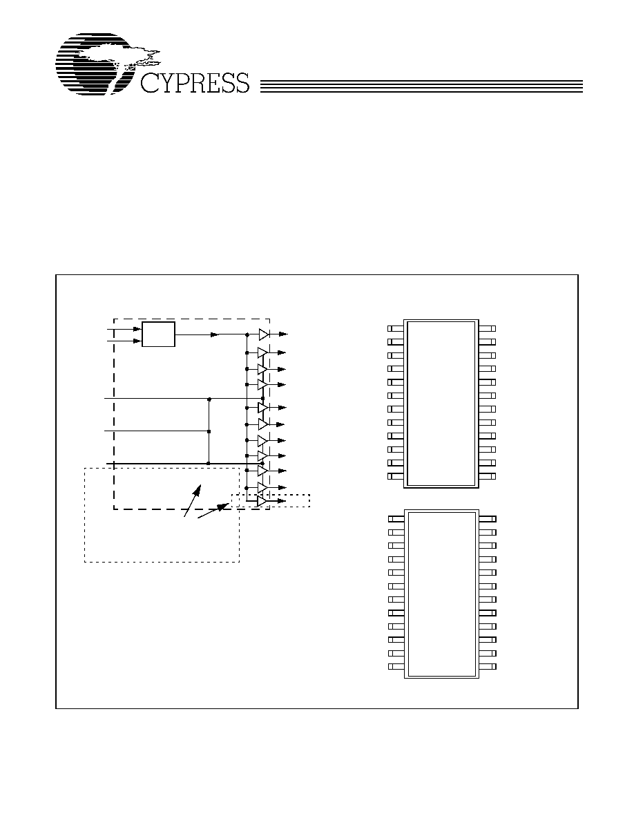
Block Diagram
Pin Configurations
CLK
AVDD
VDD
Q8
Q7
GND
GND
Q6
Q5
VDD
OE5:8
FBIN
24
23
22
21
20
19
18
17
16
15
14
13
AGND
VDD
Q0
Q1
Q2
GND
GND
Q3
Q4
VDD
OE0:4
FBOUT
1
2
3
4
5
6
7
8
9
10
11
12
:
4
3//
4
4
4
4
4
2(
4
4
)%287
4
4
2(
2(
&RQILJXUDWLRQ RI WKHVH EORFNV GHSHQGHQW XSRQ VSHFLILF RSWLRQ EHLQJ XVHG
)%,1
&/.
&/.
$9''
9''
4
4
*1'
*1'
4
4
4
9''
)%,1
$*1'
9''
4
4
4
*1'
*1'
4
4
9''
2(
)%287
:
W232
2
Overview
The W232 is a PLL-based clock driver designed for use in
systems requiring a large number of synchronous timing sig-
nals. The clock driver has output frequencies of up to 140 MHz
and output-to-output skews of less than 100 ps. The W232
provides minimum cycle-to-cycle and long-term jitter, which is
of significant importance to meet the tight input-to-input skew
budget in DIMM applications.
The W232 was specifically designed to accept SSFTG signals
currently being used in motherboard designs to reduce EMI.
Zero delay buffers which are not designed to pass this feature
through may cause skewing failures.
Output enable pins allow for shutdown of output when they are
not being used. This reduces EMI and power consumption.
Pin Definitions
Pin
Name
Pin No.
(-09)
Pin No.
(-10)
Pin
Type
Pin Description
CLK
24
24
I
Reference Input: Output signals Q0:9 will be synchronized to this signal.
FBIN
13
13
I
Feedback Input: This input must be fed by one of the outputs (typically
FBOUT) to ensure proper functionality. If the trace between FBIN and FBOUT
is equal in length to the traces between the outputs and the signal destina-
tions, then the signals received at the destinations will be synchronized to the
CLK signal input.
Q0:8
3, 4, 5, 8,
9, 16, 17,
20, 21
3, 4, 5, 8,
9, 15, 16,
17, 20, 21
O
Outputs: The frequency and phase of the signals provided by these pins will
be equal to the reference signal if properly laid out.
FBOUT
12
12
O
Feedback Output: Typically this is connected directly to the FBIN input with
a trace equal in length to the traces between outputs Q0:9 and the destination
points of these output signals.
AVDD
23
23
P
Analog Power Connection: Connect to 3.3V. Use ferrite beads to help re-
duce noise for optimal jitter performance.
AGND
1
1
G
Analog Ground Connection: Connect to common system ground plane.
VDD
2, 10, 15,
22
2, 10, 14
22
P
Power Connections: Connect to 3.3V. Use ferrite beads to help reduce
noise for optimal jitter performance.
GND
6, 7, 18,
19
6, 7, 18,
19
G
Ground Connections: Connect to common system ground plane.
OE0:4
11
--
I
Output Enable Input: Tie to V
DD
(HIGH, 1) for normal operation. When
brought to GND (LOW, 0) outputs Q0:4 are disabled to a LOW state.
OE
--
11
I
Output Enable Input: Tie to V
DD
(HIGH, 1) for normal operation. When
brought to GND (LOW, 0) outputs Q0:9 are disabled to a LOW state.
OE5:8
14
--
I
Output Enable Input: Tie to V
DD
(HIGH, 1) for normal operation. When
brought to GND (LOW, 0) outputs Q5:8 are disabled to a LOW state.
W232
3
Spread AwareTM
Many systems being designed now utilize a technology called
Spread Spectrum Frequency Timing Generation. Cypress has
been one of the pioneers of SSFTG development, and we de-
signed this product so as not to filter off the Spread Spectrum
feature of the Reference input, assuming it exists. When a zero
delay buffer is not designed to pass the SS feature through,
the result is a significant amount of tracking skew which may
cause problems in systems requiring synchronization.
For more details on Spread Spectrum timing technology,
please see the Cypress application note titled, "EMI Suppres-
sion Techniques with Spread Spectrum Frequency Timing
Generator (SSFTG) ICs."
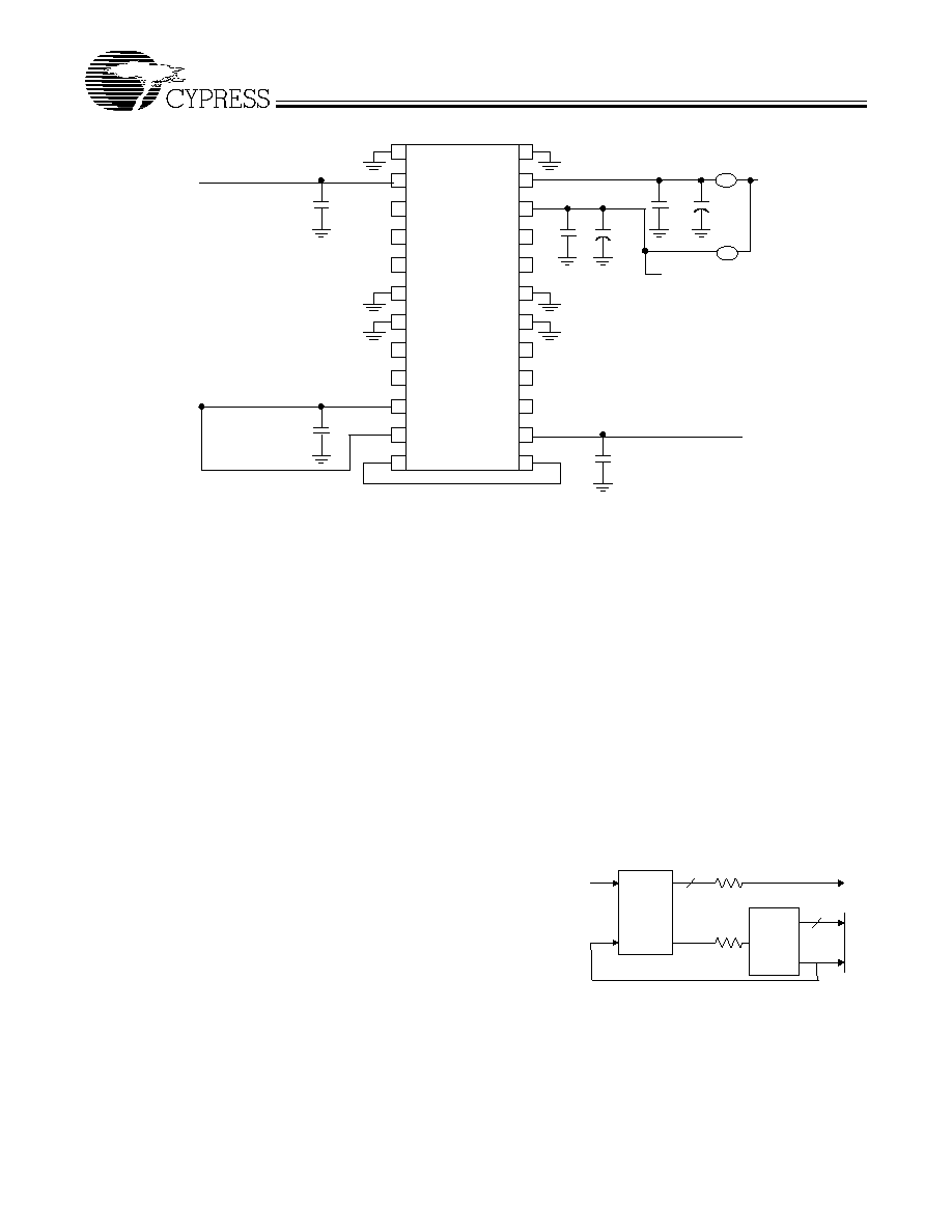
How to Implement Zero Delay
Typically, Zero Delay Buffers (ZDBs) are used because a de-
signer wants to provide multiple copies of a clock signal in
phase with each other. The whole concept behind ZDBs is that
the signals at the destination chips are all going HIGH at the
same time as the input to the ZDB. In order to achieve this,
layout must compensate for trace length between the ZDB and
the target devices. The method of compensation is described
below.
External feedback is the trait that allows for this compensation.
Since the PLL on the ZDB will cause the feedback signal to be
in phase with the reference signal. When laying out the board,
match the trace lengths between the output being used for
feed back and the FBIN input to the PLL.
If it is desirable to either add a little delay, or slightly precede
the input signal, this may also be affected by either making the
trace to the FBIN pin a little shorter or a little longer than the
traces to the devices being clocked.
Inserting Other Devices in Feedback Path
Another nice feature available due to the external feedback is
the ability to synchronize signals up to the signal coming from
some other device. This implementation can be applied to any
device (ASIC, multiple output clock buffer/driver, etc.) which is
put into the feedback path.
Referring to Figure 2, if the traces between the ASIC/buffer
and the destination of the clock signal(s) (A) are equal in length
to the trace between the buffer and the FBIN pin, the signals
at the destination(s) device will be driven HIGH at the same
time the Reference clock provided to the ZDB goes HIGH.
Synchronizing the other outputs of the ZDB to the outputs form
the ASIC/Buffer is more complex however, as any propagation
delay in the ASIC/Buffer must be accounted for.
*1'
*1'
*1'
*1'
$*1'
)%,1
9''
4
4
4
4
4
9''
$9''
*1'
)%287
2(
9''
4
4
4
4
4
9''
'
9''
0.1
µ
'
0.1
µ
'
0.1
µ
10
µ
'
10
µ
)%
)%
0.1
µ
0.1
µ
Figure 1. Schematic
:
5HIHUHQFH
6LJQDO
)HHGEDFN
,QSXW
$6,&
%XIIHU
=HUR
'HOD\
%XIIHU
$
Figure 2. 6 Output Buffer in the Feedback Path
W232
4
Absolute Maximum Ratings
Stresses greater than those listed in this table may cause per-
manent damage to the device. These represent a stress rating
only. Operation of the device at these or any other conditions
above those specified in the operating sections of this specifi-
cation is not implied. Maximum conditions for extended peri-
ods may affect reliability.
.
Parameter
Description
Rating
Unit
V
DD
, V
IN
Voltage on any Pin with Respect to GND
0.5 to +7.0
V
T
STG
Storage Temperature
65 to +150
°C
T
A
Operating Temperature
0 to +70
°C
T
B
Ambient Temperature under Bias
55 to +125
°C
P
D
Power Dissipation
0.5
W
DC Electrical Characteristics
: T
A
=0°C to 70°C, V
DD
= 3.3V ±10%
Parameter
Description
Test Condition
Min.
Typ.
Max.
Unit
I
DD
Supply Current
Unloaded, 100 MHz
200
mA
V
IL
Input Low Voltage
0.8
V
V
IH
Input High Voltage
2.0
V
V
OL
Output Low Voltage
I
OL
= 12 mA
0.8
V
V
OH
Output High Voltage
I
OH
= 12 mA
2.1
V
I
IL
Input Low Current
V
IN
= 0V
50
µ
A
I
IH
Input High Current
V
IN
= V
DD
50
µ
A
AC Electrical Characteristics:
T
A
= 0°C to +70°C, V
DD
= 3.3V ±10%
Parameter
Description
Test Condition
Min.
Typ.
Max.
Unit
f
OUT
Output Frequency
30-pF load
[4]
25
140
MHz
t
R
Output Rise Time
0.8V to 2.0V, 30-pF load
2.1
ns
t
F
Output Fall Time
2.0V to 0.8V, 30-pF load
2.5
ns
tI
CLKR
Input Clock Rise Time
[1]
4.5
ns
tI
CLKF
Input Clock Fall Time
[1]
4.5
ns
t
PEJ
CLK to FBIN Skew Variation
[2, 3]
Measured at V
DD
/2
350
0
350
ps
t
SK
Output to Output Skew
All outputs loaded equally
100
0
100
ps
t
D
Duty Cycle
30-pF load
43
50
58
%
t
LOCK
PLL Lock Time
Power supply stable
1.0
ms
t
JC
Jitter, Cycle-to-Cycle
[5]
150
ps
Notes:
1.
Longer input rise and fall time will degrade skew and jitter performance.
2.
Skew is measured at V
DD
/2 on rising edges.
3.
Duty cycle is measured at V
DD
/2.
4.
Production tests are run at 133 MHz.
5.
For frequencies below 40 MHz, Cycle-to-Cycle Jitter degrades to 175 ps.
Ordering Information
Ordering
Code
Option Number
Package Type
W232
-09, -10
24-pin TSSOP
Document #: 38-00827-C
W232
© Cypress Semiconductor Corporation, 2000. The information contained herein is subject to change without notice. Cypress Semiconductor Corporation assumes no responsibility for the use
of any circuitry other than circuitry embodied in a Cypress Semiconductor product. Nor does it convey or imply any license under patent or other rights. Cypress Semiconductor does not authorize
its products for use as critical components in life-support systems where a malfunction or failure may reasonably be expected to result in significant injury to the user. The inclusion of Cypress
Semiconductor products in life-support systems application implies that the manufacturer assumes all risk of such use and in doing so indemnifies Cypress Semiconductor against all charges.
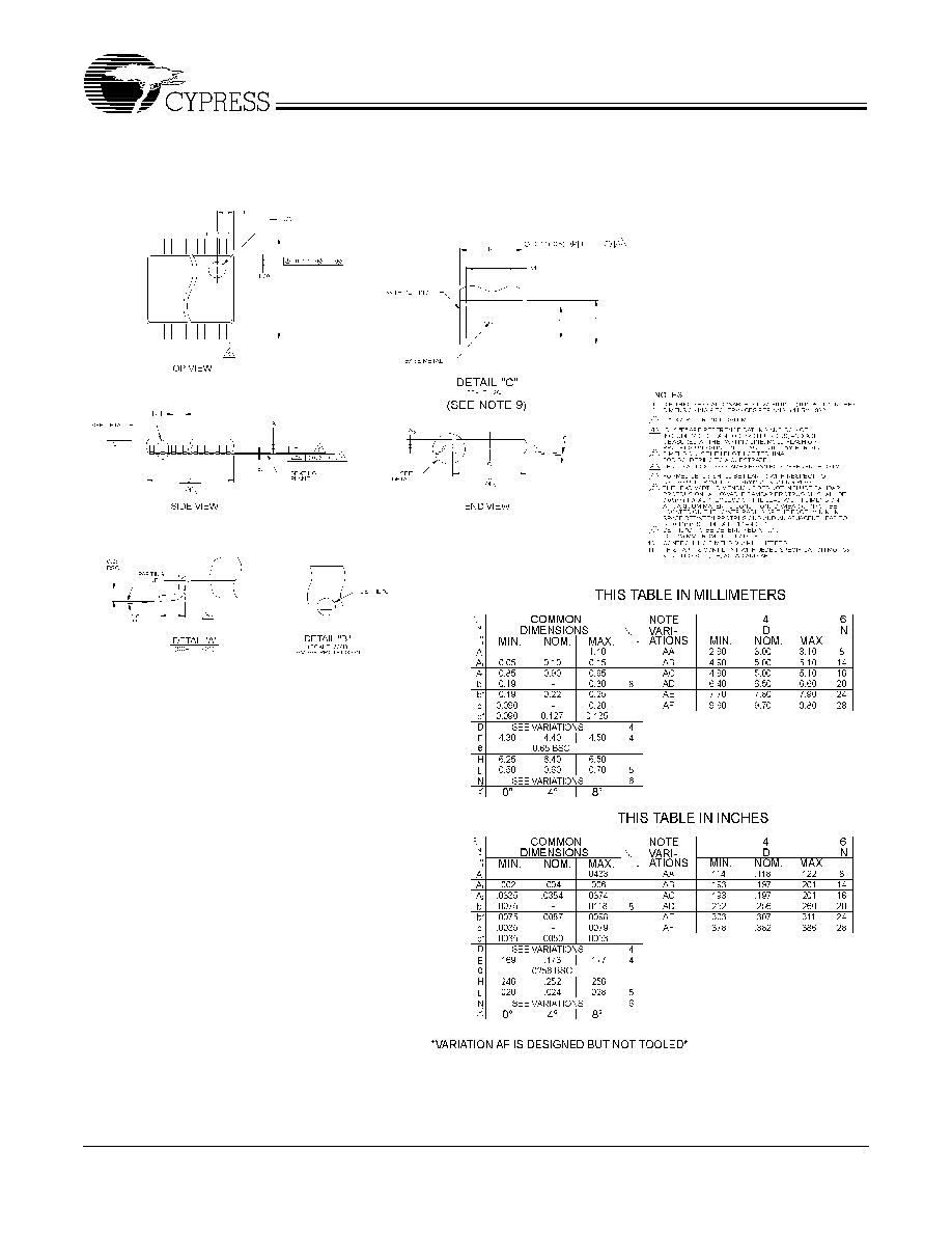
Package Diagram
24-Pin Thin Shrink Small Outline Package (TSSOP)