 | –≠–ª–µ–∫—Ç—Ä–æ–Ω–Ω—ã–π –∫–æ–º–ø–æ–Ω–µ–Ω—Ç: W305B | –°–∫–∞—á–∞—Ç—å:  PDF PDF  ZIP ZIP |
Frequency Controller with System Recovery
for Intel
Integrated Core Logic
W305B
Cypress Semiconductor Corporation
∑
3901 North First Street
∑
San Jose
,
CA 95134
∑
408-943-2600
Document #: 38-07262 Rev. *B
Revised September 1, 2004
Features
∑ Single chip FTG solution for Intel Solano/810E/810
∑ Programmable clock output frequency with less than
1 MHz increment
∑ Integrated fail-safe Watchdog timer for system
recovery
∑ Automatically switch to HW selected or SW
programmed clock frequency when Watchdog timer
time-out
∑ Capable of generating system RESET after a Watchdog
timer time-out occurs or a change in output frequency
via SMBus interface
∑ Support SMBus byte read/write and block read/write
operations to simplify system BIOS development
∑ Vendor ID and Revision ID support
∑ Programmable drive strength for SDRAM and PCI
output clocks
∑ Programmable output skew between CPU, AGP, PCI
and SDRAM
∑ Maximized EMI suppression using Cypress's Spread
Spectrum Technology
∑ Low jitter and tightly controlled clock skew
∑ Two copies of CPU clock
∑ Thirteen copies of SDRAM clock
∑ Eight copies of PCI clock
∑ One copy of synchronous APIC clock
∑ Three copies of 66-MHz outputs
∑ Three copies of 48-MHz outputs
∑ One copy of double strength 14.31818-MHz reference
clock
∑ One RESET output for system recovery
∑ SMBus interface for turning off unused clocks
Key Specifications
CPU, SDRAM Outputs Cycle-to-Cycle Jitter: ............. 250 ps
APIC, 48-MHz, 3V66, PCI Outputs
Cycle-to-Cycle Jitter:................................................... 500 ps
CPU, 3V66 Output Skew: ........................................... 175 ps
SDRAM, APIC, 48-MHz Output Skew: ....................... 250 ps
PCI Output Skew: ....................................................... 500 ps
CPU to SDRAM Skew (@ 133 MHz) ....................... ± 0.5 ns
CPU to SDRAM Skew (@ 100 MHz) ................. 4.5 to 5.5 ns
CPU to 3V66 Skew (@ 66 MHz)........................ 7.0 to 8.0 ns
3V66 to PCI Skew (3V66 lead) .......................... 1.5 to 3.5 ns
PCI to APIC Skew..................................................... ± 0.5 ns
1. Internal 100K pull-up and 100K pull-down resistors present on inputs marked with * and ^ respectively. Design should not rely solely on internal pull-up resistor
to set I/O pins HIGH or LOW.
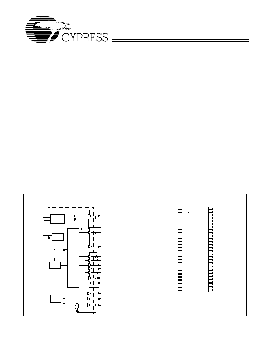
Block Diagram
Pin Configuration
[1]
VDDQ3
VDDQ2
PCI1/FS1
XTAL
PLL REF FREQ
PLL 1
X2
X1
REF2X/FS3
PCI3:7
48MHz/FS4
24_48MHz/SEL24_48MHz#
PLL2
OSC
VDDQ3
SMBus
SDATA
Logic
SCLK
3V66_0:2
CPU0:1
APIC
Divider,
Delay,
and
Phase
Control
Logic
3
VDDQ3
2
SDRAM0:12
13
RST#
PCI0/FS0
PCI2/FS2
/2
(FS0:4)
5
48MHz
GND
VDDQ3
REF2X/FS3^
X1
X2
VDDQ3
3V66_0
3V66_1
3V66_2
GND
PCI0/FS0^
PCI1/FS1^
PCI2/FS2^
GND
PCI3
PCI4
VDDQ3
PCI5
PCI6
PCI7
GND
48MHz
48MHz/FS4^
24_48MHz/SEL24_48MHz#*
W
305B
VDDQ2
APIC
GND
VDDQ2
CPU0
CPU1
GND
SDRAM0
SDRAM1
SDRAM2
VDDQ3
GND
SDRAM3
SDRAM4
SDRAM5
SDRAM6
VDDQ3
GND
SDRAM7
SDRAM8
SDRAM9
SDRAM10
VDDQ3
GND
56
55
54
53
52
51
50
49
48
47
46
45
44
43
42
41
40
39
38
37
36
35
34
33
1
2
3
4
5
6
7
8
9
10
11
12
13
14
15
16
17
18
19
20
21
22
23
24
25
26
27
28
32
31
30
29
VDDQ3
SDATA
GND
VDDQ3
SDRAM11
SDRAM12
RST#
SCLK

W305B
Document #: 38-07262 Rev. *B
Page 2 of 21
Pin Definitions
Pin Name
Pin No.
Pin
Type
Pin Description
REF2X/FS3
3
I/O
Reference Clock with 2x Drive/Frequency Select 3. 3.3V 14.318-MHz clock
output. This pin also serves as the select strap to determines device operating
frequency as described in Table 5.
X1
4
I
Crystal Input. This pin has dual functions. It can be used as an external
14.318-MHz crystal connection or as an external reference frequency input.
X2
5
O
Crystal Output. An input connection for an external 14.318-MHz crystal
connection. If using an external reference, this pin must be left unconnected.
PCI0/FS0
11
I/O
PCI Clock 0/Frequency Selection 0. 3.3V 33-MHz PCI clock outputs. This pin
also serves as the select strap to determine device operating frequency as
described in Table 5.
PCI1/FS1
12
I/O
PCI Clock 1/Frequency Selection 1. 3.3V 33-MHz PCI clock outputs. This pin
also serves as the select strap to determine device operating frequency as
described in Table 5.
PCI2/FS2
13
I/O
PCI Clock 2/Frequency Selection 2. 3.3V 33-MHz PCI clock outputs. This pin
also serves as the select strap to determine device operating frequency as
described in Table 5.
PCI3:7
15, 16, 18, 19, 20
O
PCI Clock 3 through 7. 3.3V 33-MHz PCI clock outputs. PCI0:7 can be individ-
ually turned off via SMBus interface.
3V66_0:2
7, 8, 9
O
66-MHz Clock Output. 3.3V output clocks. The operating frequency is
controlled by FS0:4 (see Table 5).
48MHz
22
O
48MHz. 3.3V 48-MHz non-spread spectrum output.
48MHz/FS4
23
I/O
48-MHz Output/Frequency Selection 4. 3.3V 48-MHz non-spread spectrum
output. This pin also serves as the select strap to determine device operating
frequency as described in Table 5.
24_48MHz/SEL24
_48MHz#
24
I/O
24- or 48-MHz Output/Select 24 or 48MHz. 3.3V 24 or 48-MHz non-spread
spectrum output. This pin also serves as the select strap to determine the output
frequency for 24_48MHz output.
RST#
30
O
(open-d
rain)
Reset#. Open-drain RESET# output.
CPU0:1
52, 51
O
CPU Clock Outputs. Clock outputs for the host bus interface. Output
frequencies depending on the configuration of FS0:4. Voltage swing is set by
VDDQ2.
SDRAM0:12,
49, 48, 47, 44,
43, 42, 41, 38,
37, 36, 35, 32, 31
O
SDRAM Clock Outputs. 3.3V outputs for SDRAM and chipset. The operating
frequency is controlled by FS0:4 (see Table 5).
APIC
55
O
Synchronous APIC Clock Outputs. Clock outputs running synchronous with
the PCI clock outputs. Voltage swing set by VDDQ2.
SDATA
26
I/O
Data pin for SMBus circuitry.
SCLK
29
I
Clock pin for SMBus circuitry.
VDDQ3
2, 6, 17, 25, 28,
34, 40, 46
P
3.3V Power Connection. Power supply for SDRAM output buffers, PCI output
buffers, reference output buffers and 48-MHz output buffers. Connect to 3.3V.
VDDQ2
53, 56
P
2.5V Power Connection. Power supply for APIC and CPU output buffers.
Connect to 2.5V.
GND
1, 10, 14, 21, 27,
33, 39, 45, 50, 54
G
Ground Connections. Connect all ground pins to the common system ground
plane.

W305B
Document #: 38-07262 Rev. *B
Page 3 of 21
Overview
The W305B is a highly integrated frequency timing generator,
supplying all the required clock sources for an Intel
Æ
archi-
tecture platform using graphics integrated core logic.
Functional Description
I/O Pin Operation
Upon power-up the power on strap option pins act as a logic
input. An external 10-k
strapping resistor should be used.
Figure 1 shows a suggested method for strapping resistor
connections.
After 2 ms, the pin becomes an output. Assuming the power
supply has stabilized by then, the specified output frequency
is delivered on the pins. If the power supply has not yet
reached full value, output frequency initially may be below
target but will increase to target once supply voltage has stabi-
lized. In either case, a short output clock cycle may be
produced from the CPU clock outputs when the outputs are
enabled.
Offsets Among Clock Signal Groups
Figure 2, Figure 3, and Figure 4 represent the phase
relationship among the different groups of clock outputs from
W305B under different frequency modes.
Power-on
Reset
Timer
Output Three-state
Data
Latch
Hold
Q
D
W305B
Clock Load
Output
Buffer
10 k
Output
Low
Output Strapping Resistor
Series Termination Resistor
Figure 1. Input Logic Selection Through Resistor Load Option
Figure 2. Group Offset Waveforms (66-MHz CPU Clock, 100-MHz SDRAM Clock)
CPU 66-MHz
SDRAM 100-MHz
3V66 66-MHz
PCI 33-MHz
REF 14.318-MHz
USB 48-MHz
APIC 16.6-MHz
0 ns
CPU 66 Period
SDRAM 100 Period
Hub-PCI
40 ns
30 ns
20 ns
10 ns

W305B
Document #: 38-07262 Rev. *B
Page 4 of 21
CPU 100-MHz
SDRAM 100-MHz
3V66 66-MHz
PCI 33-MHz
REF 14.318-MHz
USB 48-MHz
APIC16.6-MHz
0 ns
Figure 3. Group Offset Waveforms (100-MHz CPU Clock, 100-MHz SDRAM Clock)
40 ns
30 ns
20 ns
10 ns
SDRAM 100 Period
CPU 100 Period
Hub-PC
CPU 133-MHz
SDRAM 100-MHz
3V66 66-MHz
PCI 33-MHz
REF 14.318-MHz
USB 48-MHz
DOT 48-MHz
0 ns 10 ns 20 ns 30 ns 40 ns
Cycle Repeats
APIC 16.6-MHz
Figure 4. Group Offset Waveforms (133-MHz CPU/100-MHz SDRAM)

W305B
Document #: 38-07262 Rev. *B
Page 5 of 21
Serial Data Interface
The W305B features a two-pin, serial data interface that can
be used to configure internal register settings that control
particular device functions.
Data Protocol
The clock driver serial protocol supports byte/word write,
byte/word read, block write and block read operations from the
controller. For block write/read operation, the bytes must be
accessed in sequential order from lowest to highest byte with
the ability to stop after any complete byte has been trans-
ferred. For byte/word write and byte read operations, system
controller can access individual indexed byte. The offset of the
indexed byte is encoded in the command code.
The definition for the command code is given in Table 1.
CPU 133-MHz
SDRAM 133MHz
3V66 66-MHz
PCI 33-MHz
REF 14.318-MHz
USB 48-MHz
DOT 48-MHz
APIC 16.6-MHz
Cycle Repeat
0 ns 10 ns 20 ns 30 ns 40 ns
Figure 5. Group Offset Waveform (133-MHz CPU/133-MHz SDRAM)
Table 1. Command Code Definition
Bit
Descriptions
7
0 = Block read or block write operation
1 = Byte/Word read or byte/word write operation
6:0
Byte offset for byte/word read or write operation. For block read or write operations, these bits
need to be set at `0000000'.
Table 2. Block Read and Block Write Protocol
Block Write Protocol
Block Read Protocol
Bit
Description
Bit
Description
1
Start
1
Start
2:8
Slave address ≠ 7 bit
2:8
Slave address ≠ 7 bit
9
Write
9
Write
10
Acknowledge from slave
10
Acknowledge from slave
11:18
Command Code ≠ 8 bit
`00000000' stands for block operation
11:18
Command Code ≠ 8 bit
`00000000' stands for block operation
19
Acknowledge from slave
19
Acknowledge from slave
20:27
Byte Count ≠ 8 bits
20
Repeat start
28
Acknowledge from slave
21:27
Slave address ≠ 7 bits
29:36
Data byte 0 ≠ 8 bits
28
Read
37
Acknowledge from slave
29
Acknowledge from slave
38:45
Data byte 1 ≠ 8 bits
30:37
Byte count from slave ≠ 8 bits
46
Acknowledge from slave
38
Acknowledge
...
Data Byte N/Slave Acknowledge...
39:46
Data byte from slave ≠ 8 bits