 | –≠–ª–µ–∫—Ç—Ä–æ–Ω–Ω—ã–π –∫–æ–º–ø–æ–Ω–µ–Ω—Ç: W312-02HT | –°–∫–∞—á–∞—Ç—å:  PDF PDF  ZIP ZIP |

FTG for VIATM K7 Series Chipset with Programmable Output Frequency
W312-02
Cypress Semiconductor Corporation
∑
3901 North First Street
∑
San Jose
∑
CA 95134
∑
408-943-2600
Document #: 38-07259 Rev. *B
Revised December 19, 2002
Features
∑ Single chip FTG solution for VIATM K7 Series chipsets
∑ Programmable clock output frequency with less than
1 MHz increment
∑ Integrated fail-safe Watchdog timer for system recov-
ery
∑ Automatically switch to HW selected or SW
programmed clock frequency when watchdog timer
time-out
∑ Capable of generate system RESET after a watchdog
timer time-out occurs or a change in output frequency
via SMBus interface
∑ Support SMBus byte read/write and block read/ write
operations to simplify system BIOS development
∑ Vendor ID and Revision ID support
∑ Programmable drive strength for PCI output clocks
∑ Programmable output skew between CPU, AGP and PCI
∑ Maximized EMI suppression using Cypress's Spread
Spectrum technology
∑ Low jitter and tightly controlled clock skew
∑ Two pairs of differential CPU clocks
∑ Eleven copies of PCI clocks
∑ Three copies of 66-MHz outputs
∑ Two copies of 48-MHz outputs
∑ Three copies of 14.31818-MHz reference clocks
∑ One RESET output for system recovery
∑ Power management control support
Key Specifications
CPU Outputs Cycle-to-cycle Jitter: ............................. 250 ps
48-MHz, 3V66, PCI Outputs
Cycle-to-cycle Jitter: .................................................... 500 ps
CPU, 3V66 Output Skew: ............................................ 200 ps
48-MHz Output Skew: ................................................. 250 ps
PCI Output Skew: ........................................................ 500 ps
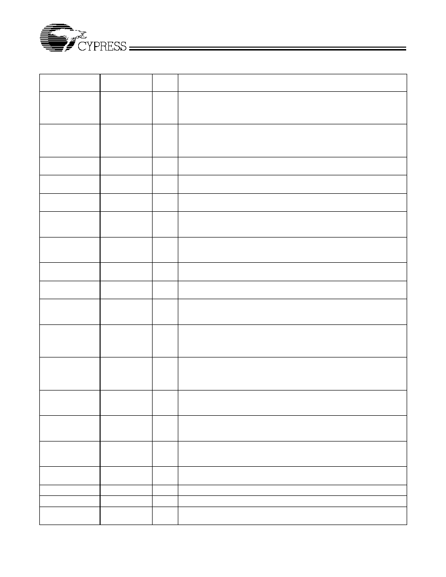
Block Diagram
Pin Configuration
Note:
1.
Internal 100K pull-up resistors present on inputs marked with *. De-
sign should not rely solely on internal pull-up resistor to set I/O pins
HIGH.
[1]
VDD_REF
VDD_CPU
PCI1:8
XTAL
PLL REF FREQ
PLL 1
X2
X1
REF2
24_48MHz/FS4*
PLL2
OSC
VDD_48MHz
SMBus
SDATA
Logic
SCLK
AGP0:2
CPUT0,CPUC0
CPUT_CS,CPUC_CS
Divider,
Delay,
and
Phase
Control
Logic
3
VDD_PCI
2
RST#
PCI0/SEL24_48#*
PCI9_E
/2
(FS0:4)
5
48MHz/FS3*
VDD_REF
GND_REF
X1
X2
VDD_48MHz
*FS2/48MHz
*FS3/24_48MHz
GND_48MHz
*FS4/PCI_F
*SEL24_48#/PCI0
PCI1
GND_PCI
PCI2
PCI3
VDD_PCI
PCI4
PCI5
PCI6
GND_PCI
PCI7
PCI8
PCI9_E
VDD_PCI
RST#
W3
12-02
REF0/FS0*
REF1/FS1*
REF2
REF_STOP#*
AGP_STOP#*
GND_CPU
CPUT0
CPUC0
VDD_CPU
CPUT_CS
CPUC_CS
GND_CPU
CPU_STOP#*
PCI_STOP#*
PD#*
VDD_CORE
GND_CORE
SDATA
SCLK
GND_AGP
AGP2
AGP1
AGP0
VDD_AGP
48
47
46
45
44
43
42
41
40
39
38
37
36
35
34
33
32
31
30
29
28
27
26
25
1
2
3
4
5
6
7
8
9
10
11
12
13
14
15
16
17
18
19
20
21
22
23
24
REF1/FS1*
REF0/FS0*
VDD_AGP
SEL24_48#*
PD#
CPU_STOP#
PCI_STOP#
AGP_STOP#
REF_STOP#
W312-02
Document #: 38-07259 Rev. *B
Page 2 of 21
I
Pin Definitions
Pin Name
Pin No.
Pin
Type
Pin Description
REF0/FS0
48
I/O
Reference Clock Output 0/Frequency Select 0: 3.3V 14.318-MHz clock out-
put. REF0 will be disabled when REF_STOP# is active. This pin also serves
as the select strap to determines device operating frequency as described in
Table 4.
REF1/FS1
47
I/O
Reference Clock Output 0/Frequency Select 1: 3.3V 14.318-MHz clock out-
put. REF1 will be disabled when REF_STOP# is active. This pin also serves
as the select strap to determines device operating frequency as described in
Table 4.
REF2
46
I/O
Reference Clock Output 2: 3.3V 14.318-MHz clock output. REF2 will be dis-
abled when REF_STOP# is active.
X1
3
I
Crystal Input: This pin has dual functions. It can be used as an external
14.318-MHz crystal connection or as an external reference frequency input.
X2
4
I
Crystal Output: An input connection for an external 14.318-MHz crystal con-
nection. If using an external reference, this pin must be left unconnected.
PCI_F/FS4
9
I
Free-Running PCI Clock/Frequency Select 4: 3.3V 33-MHz free running PCI
clock output. This pin also serves as the select strap to determines device
operating frequency as described in Table 4.
PCI_0/SEL24_48#
10
I/O
PCI Clock 0/Select 24 or 48 MHz: 3.3V 33-MHz PCI clock outputs. This output
will be disabled when PCI_STOP# is active. This pin also serves as the select
strap to determine device operating frequency of 24_48MHz output.
PCI1:8
11, 13, 14, 16,
17, 18, 20, 21
O
PCI Clock 1 through 8: 3.3V 33-MHz PCI clock outputs. PCI1:8 will be dis-
abled when PCI_STOP# is active.
PCI9_E
22
O
Early PCI Clock 9: 3.3V 33-MHz PCI clock outputs. PCI9_E will be disabled
when PCI_STOP# is active.
AGP0:2
26, 27, 28
O
AGP Clock 0 through 2: 3.3V 66-MHz clock outputs. The operating frequency
is controlled by FS0:4 (see Table 4). AGP0:2 will be disabled when
AGP_STOP# is active.
48MHz/FS2
6
I/O
48-MHz Output/Frequency Selection 3: 3.3V 48-MHz non-spread spectrum
output. 48MHz will be disabled when REF_STOP# is active. This pin also
serves as the select strap to determine device operating frequency as de-
scribed in Table 4.
24_48MHz/FS3
7
I/O
24 or 48-MHz Output/Select 24 or 48 MHz: 3.3V 24 or 48-MHz non-spread
spectrum output. 24_48MHz will be disabled when REF_STOP# is active. This
pin also serves as the select strap to determine device operating frequency as
described in Table 4.
RST#
24
O
(open-
drain)
Reset#: Open-drain RESET# output.
CPUT0, CPUC0
42, 41
O
(open-
drain)
CPU Clock Output 0: CPUT0 and CPUC0 are the differential CPU clock out-
puts for the K7 processor. They are open-drain outputs.
CPUT_CS,
CPUC_CS
39, 38
O
CPU Clock Output for Chipset: CPUT_CS and CPUC_CS are the differential
CPU clock outputs for the chipset. They are push-pull outputs. These outputs
will be disabled when CPU_STOP# is active.
CPU_STOP#
36
I
CPU STOP Input: This input will disable CPUT_CS and CPUC_CS when it is
active.
PCI_STOP#
35
I
PCI STOP Input: This input will disable PCI0:8 and PCI9_E when it is active.
AGP_STOP#
44
I
AGP STOP Input: This input will disable AGP0:2 when it is active.
REF_STOP#
45
I
REF STOP Input: This input will disable REF0:2, 24_48MHz and 48 MHz
outputs when it is active.

W312-02
Document #: 38-07259 Rev. *B
Page 3 of 21
PD#
34
I
Power-Down Input: This input will trigger the clock generator into Power
Down mode when it is active.
SDATA
31
I/O
Data pin for SMBus circuitry.
SCLK
30
I
Clock pin for SMBus circuitry.
VDD_CPU
40
P
2.5V Power Connection: Power supply for CPU output buffers. Connect to
2.5V.
VDDQ_AGP
25
P
3.3V Power Connection: Power supply for AGP output buffers. Connect to
3.3V.
VDDQ_PCI
15, 23
P
3.3V Power Connection: Power supply for PCI output buffers. Connect to
3.3V.
VDDQ_48MHz
5
P
3.3V Power Connection: Power supply for 48 MHz output buffers. Connect
to 3.3V.
VDD_REF
1
P
3.3V Power Connection: Power supply for reference output buffers. Connect
to 3.3V.
VDD_Core
33
P
3.3V Power Connection: Power supply for PLL core. Connect to 3.3V.
GND_REF,
GND_48MHz,
GND_PCI,
GND_AGP,
GND_Core,
GND_CPU
2, 8, 29, 32, 37,
43
G
Ground Connections: Connect all ground pins to the common system ground
plane.
Pin Definitions
(continued)
Pin Name
Pin No.
Pin
Type
Pin Description

W312-02
Document #: 38-07259 Rev. *B
Page 4 of 21
Serial Data Interface
The W312-02 features a two-pin, serial data interface that can
be used to configure internal register settings that control par-
ticular device functions.
Data Protocol
The clock driver serial protocol supports byte/word write,
byte/word read, block write and block read operations from the
controller. For block write/read operation, the bytes must be
accessed in sequential order from lowest to highest byte with
the ability to stop after any complete byte has been trans-
ferred. For byte/word write and byte read operations, system
controller can access individual indexed byte. The offset of the
indexed byte is encoded in the command code.
The definition for the command code is defined in Table 1.
Bit
Descriptions
7
0 = Block read or block write operation
1 = Byte/Word read or byte/word write operation
6:0
Byte offset for byte/word read or write operation. For block read or write operations, these bits
need to be set at `0000000'.
Table 1. Block Read and Block Write Protocol
Block Write Protocol
Block Read Protocol
Bit
Description
Bit
Description
1
Start
1
Start
2:8
Slave address ≠ 7 bits
2:8
Slave address ≠ 7 bits
9
Write
9
Write
10
Acknowledge from slave
10
Acknowledge from slave
11:18
Command Code ≠ 8 bits
`00000000' stands for block operation
11:18
Command Code ≠ 8 bits
`00000000' stands for block operation
19
Acknowledge from slave
19
Acknowledge from slave
20:27
Byte Count ≠ 8 bits
20
Repeat start
28
Acknowledge from slave
21:27
Slave address ≠ 7 bits
29:36
Data byte 0 ≠ 8 bits
28
Read
37
Acknowledge from slave
29
Acknowledge from slave
38:45
Data byte 1 ≠ 8 bits
30:37
Byte count from slave ≠ 8 bits
46
Acknowledge from slave
38
Acknowledge
...
Data Byte N/Slave Acknowledge...
39:46
Data byte from slave ≠ 8 bits
...
Data Byte N ≠ 8 bits
47
Acknowledge
...
Acknowledge from slave
48:55
Data byte from slave ≠ 8 bits
...
Stop
56
Acknowledge
...
Data bytes from slave/Acknowledge
...
Data byte N from slave ≠ 8 bits
...
Not Acknowledge
...
Stop
W312-02
Document #: 38-07259 Rev. *B
Page 5 of 21
Table 2. Word Read and Word Write Protocol
Word Write Protocol
Word Read Protocol
Bit
Description
Bit
Description
1
Start
1
Start
2:8
Slave address ≠ 7 bits
2:8
Slave address ≠ 7 bits
9
Write
9
Write
10
Acknowledge from slave
10
Acknowledge from slave
11:18
Command Code ≠ 8 bits
`1xxxxxxx' stands for byte or word operation
bit[6:0] of the command code represents the off-
set of the byte to be accessed
11:18
Command Code ≠ 8 bits
`1xxxxxxx' stands for byte or word operation
bit[6:0] of the command code represents the off-
set of the byte to be accessed
19
Acknowledge from slave
19
Acknowledge from slave
20:27
Data byte low ≠ 8 bits
20
Repeat start
28
Acknowledge from slave
21:27
Slave address ≠ 7 bits
29:36
Data byte high ≠- 8 bits
28
Read
37
Acknowledge from slave
29
Acknowledge from slave
38
Stop
30:37
Data byte low from slave ≠ 8 bits
38
Acknowledge
39:46
Data byte high from slave ≠ 8 bits
47
NOT acknowledge
48
Stop
Table 3. Byte Read and Byte Write Protocol
Byte Write Protocol
Byte Read Protocol
Bit
Description
Bit
Description
1
Start
1
Start
2:8
Slave address ≠ 7 bits
2:8
Slave address ≠ 7 bits
9
Write
9
Write
10
Acknowledge from slave
10
Acknowledge from slave
11:18
Command Code ≠ 8 bits
`1xxxxxxx' stands for byte operation
bit[6:0] of the command code represents the off-
set of the byte to be accessed
11:18
Command Code ≠ 8 bits
`1xxxxxxx' stands for byte operation
bit[6:0] of the command code represents the off-
set of the byte to be accessed
19
Acknowledge from slave
19
Acknowledge from slave
20:27
Data byte ≠ 8 bits
20
Repeat start
28
Acknowledge from slave
21:27
Slave address ≠ 7 bits
29
Stop
28
Read
29
Acknowledge from slave
30:37
Data byte from slave ≠ 8 bits
38
Not Acknowledge
39
Stop