/home/web/doc/html/cypress/205515
Spread Spectrum BX System Frequency Generator
W48C101-01
Cypress Semiconductor Corporation
·
3901 North First Street
·
San Jose
·
CA 95134
·
408-943-2600
Document #: 38-07192 Rev. *A
Revised December 22, 2002
01-01
Features
· Maximized EMI suppression using Cypress's Spread
Spectrum technology
· Four copies of CPU output
· Eight copies of PCI output (Synchronous w/CPU
output)
· Two copies of 14.318-MHz IOAPIC output
· Two copies of 48-MHz USB output
· Three buffered copies of 14.318-MHz reference input
· Input is a 14.318-MHz XTAL or reference signal
· Selectable 100-MHz or 66-MHz CPU outputs
· Power management control input pins
· Test mode and output three-state capability
Key Specifications
Supply Voltages: ....................................... V
DDQ3
= 3.3V±5%
V
DDQ2
= 2.5V±5% or 3.3V±5%
CPU0:3 Jitter (Cycle to Cycle): ................................... 200 ps
CPU0:3 Clock Skew: ................................................... 175 ps
PCI_F, PCI1:7 Clock Skew: .........................................500 ps
CPU to PCI Clock Skew: .............. 1.5 to 4.0 ns (CPU Leads)
Logic inputs have 250-k
pull-up resistors except
SEL100/66#.
Table 1. Pin Selectable Frequency
SEL
100/66#
SEL1
SEL0
CPU
(MHz)
PCI
(MHz)
SPREAD#=0
0
0
0
HI-Z
HI-Z
Don't Care
0
0
1
66.6
33.3
±0.9% Center
0
1
0
66.6
33.3
1% Down
0
1
1
66.6
33.3
0.5% Down
1
0
0
X1/2
X1/6
Don't Care
1
0
1
100
33.3
±0.9% Center
1
1
0
100
33.3
1% Down
1
1
1
100
33.3
0.5% Down
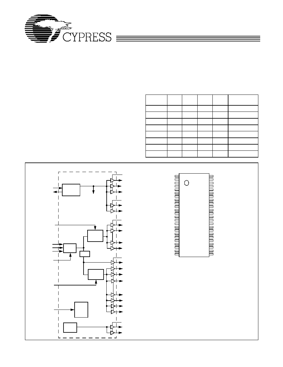
Pin Configuration
Block Diagram
REF0
REF1
GND
X1
X2
GND
PCI_F
PCI1
VDDQ3
PCI2
PCI3
GND
PCI4
PCI5
VDDQ3
PCI6
PCI7
GND
VDDQ3
GND
VDDQ3
48MHz
48MHz
GND
VDDQ3
REF2
VDDQ2
APIC0
APIC1
GND
NC
VDDQ2
CPU0
CPU1
GND
VDDQ2
CPU2
CPU3
GND
VDDQ3
GND
PCI_STOP#
CPU_STOP#
PWR_DWN#
SPREAD#
SEL0
SEL1
SEL100/66#
48
47
46
45
44
43
42
41
40
39
38
37
36
35
34
33
32
31
30
29
28
27
26
25
1
2
3
4
5
6
7
8
9
10
11
12
13
14
15
16
17
18
19
20
21
22
23
24
VDDQ3
REF0
VDDQ2
APIC0
CPU0
CPU1
CPU2
CPU3
PCI_F
XTAL
PLL Ref Freq
PLL 1
SEL100/66#
X2
X1
REF1
VDDQ3
Stop
Clock
Control
Stop
Clock
Control
PCI1
PWR_DWN#
Power
Down
Control
PCI2
PCI3
PCI4
PCI5
48MHz
48MHz
PLL2
÷2/÷3
OSC
REF2
VDDQ2
PCI_STOP#
CPU_STOP#
PCI6
PCI7
VDDQ3
APIC1
SEL0
SEL1
SPREAD#
W48C101-01
Document #: 38-07192 Rev. *A
Page 2 of 9
Pin Definitions
Pin Name
Pin
No.
Pin
Type
Pin Description
CPU0:3
40, 39, 36,
35
O
CPU Clock Outputs 0 through 3: These four CPU clock outputs are controlled by
the CPU_STOP# control pin. Output voltage swing is controlled by voltage applied
to VDDQ2.
PCI1:7
8, 10, 11, 13,
14, 16, 17
O
PCI Bus Clock Outputs 1 through 7: These seven PCI clock outputs are con-
trolled by the PCI_STOP# control pin. Output voltage swing is controlled by voltage
applied to VDDQ3.
PCI_F
7
O
Fixed PCI Clock Output: Unlike PCI1:7 outputs, this output is not controlled by the
PCI_STOP# control pin. Output voltage swing is controlled by voltage applied to
VDDQ3.
CPU_STOP#
30
I
CPU_STOP# Input: When brought LOW, clock outputs CPU0:3 are stopped LOW
after completing a full clock cycle (23 CPU clock latency). When brought HIGH,
clock outputs CPU0:3 start beginning with a full clock cycle (23 CPU clock latency).
PCI_STOP#
31
I
PCI_STOP# Input: The PCI_STOP# input enables the PCI 1:7 outputs when HIGH
and causes them to remain at logic 0 when LOW. The PCI_STOP signal is latched
on the rising edge of PCI_F. Its effects take place on the next PCI_F clock cycle.
SPREAD#
28
I
SPREAD# Input: When brought LOW this pin activates Spread Spectrum clocking.
APIC0:1
45, 44
O
I/O APIC Clock Outputs: Provides 14.318-MHz fixed frequency. The output volt-
age swing is controlled by VDDQ2.
48MHz
22, 23
O
48-MHz Outputs: Fixed clock outputs at 48 MHz. Output voltage swing is controlled
by voltage applied to VDDQ3.
REF0:2
1, 2, 47
O
Fixed 14.318-MHz Outputs 0 through 2: Used for various system applications.
Output voltage swing is controlled by voltage applied to VDDQ3.
SEL100/66#
SEL1:0
25, 26, 27
I
Frequency Selection Input: Selects power-up default CPU clock frequency as
shown in Table 1 on page 1.
X1
4
I
Crystal Connection or External Reference Frequency Input: Connect to either
a 14.318-MHz crystal or reference signal.
X2
5
I
Crystal Connection: An input connection for an external 14.318-MHz crystal. If
using an external reference, this pin must be left unconnected.
PWR_DWN#
29
I
Power Down Control: When this input is LOW, device goes into a low-power
condition. All outputs are held LOW while in power-down. CPU and PCI clock out-
puts are stopped LOW after completing a full clock cycle (23 CPU clock cycle
latency). When brought HIGH, CPU, SDRAM and PCI outputs start with a full clock
cycle at full operating frequency (3 ms maximum latency).
VDDQ3
9, 15, 19, 21,
33, 48
P
Power Connection: Connect to 3.3V supply.
VDDQ2
37,41,46
P
Power Connection: Power supply for CPU0:3 and APIC0:1 output buffers. Con-
nect to 2.5V supply or 3.3V supply.
GND
3, 6, 12, 18,
20, 24, 32,
34, 38, 43
G
Ground Connection: Connect all ground pins to the common system ground
plane.
NC
42
-
No Connect: Do not connect.
W48C101-01
Document #: 38-07192 Rev. *A
Page 3 of 9
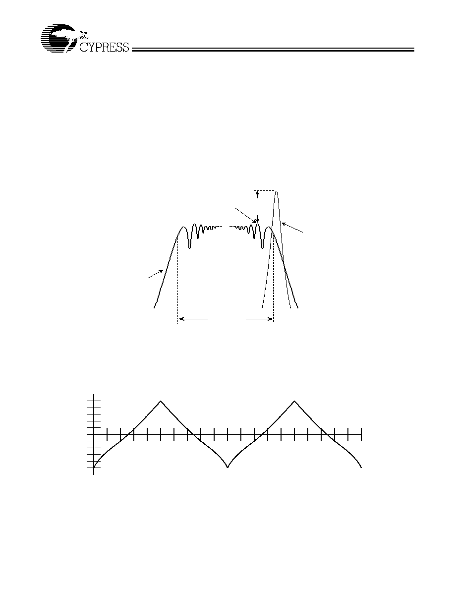
Spread Spectrum Clocking
The device generates a clock that is frequency modulated in
order to increase the bandwidth that it occupies. By increasing
the bandwidth of the fundamental and its harmonics, the am-
plitudes of the radiated electromagnetic emissions are re-
duced. This effect is depicted in Figure 1.
As shown in Figure 1, a harmonic of a modulated clock has a
much lower amplitude than that of an unmodulated signal. The
reduction in amplitude is dependent on the harmonic number
and the frequency deviation or spread. The equation for the
reduction is:
dB = 6.5 + 9*log
10
(P) + 9*log
10
(F)
Where P is the percentage of deviation and F is the frequency
in MHz where the reduction is measured.
The output clock is modulated with a waveform depicted in
Figure 2. This waveform, as discussed in "Spread Spectrum
Clock Generation for the Reduction of Radiated Emissions" by
Bush, Fessler, and Hardin produces the maximum reduction
in the amplitude of radiated electromagnetic emissions. The
deviation selected for this chip is 0.5%, 1.0%, or ±0.9% of
the selected frequency. Figure 2 details the Cypress spreading
pattern. Cypress does offer options with more spread and
greater EMI reduction. Contact your local Sales representative
for details on these devices.
Spread Spectrum clocking is activated or deactivated by se-
lecting the appropriate values for SPREAD#.
Figure 1. Clock Harmonic with and without SSCG Modulation Frequency Domain Representation
SSC
non-
SSC
Highest
of f
nom
f
nom
MAX (+0.5%)
MIN (0.5%)
10%
20%
30%
40%
50%
60%
70%
80%
90%
1
00%
10%
20%
30%
40%
50%
60%
70%
80%
90%
1
00%
FREQUENCY
Figure 2. Typical Modulation Profile
W48C101-01
Document #: 38-07192 Rev. *A
Page 4 of 9
Absolute Maximum Ratings
[1]
Stresses greater than those listed in this table may cause per-
manent damage to the device. These represent a stress rating
only. Operation of the device at these or any other conditions
above those specified in the operating sections of this specifi-
cation is not implied. Maximum conditions for extended peri-
ods may affect reliability.
Parameter
Description
Rating
Unit
V
DD
, V
IN
Voltage on any pin with respect to GND
0.5 to +7.0
V
T
STG
Storage Temperature
65 to +150
°C
T
A
Operating Temperature
0 to +70
°C
T
B
Ambient Temperature under Bias
55 to +125
°C
ESD
PROT
Input ESD Protection
2 (min.)
kV
DC Electrical Characteristics:
T
A
= 0°C to +70°C, V
DDQ3
= 3.3V±5%, V
DDQ2
= 2.5V±5%
Parameter
Description
Test Condition
Min.
Typ.
Max.
Unit
Supply Current
I
DDQ3
3.3V Supply Current
CPU0:3 = 100 MHz
Outputs Loaded
[2]
120
mA
I
DDQ2
2.5V Supply Current
CPU0:3 = 100 MHz
Outputs Loaded
[2]
65
mA
Logic Inputs
V
IL
Input Low Voltage
GND 0.3
0.8
V
V
IH
Input High Voltage
2.0
V
DD
+ 0.3
V
I
IL
Input Low Current
[3]
25
µA
I
IH
Input High Current
[3]
10
µA
I
IL
Input Low Current (SEL100/66#)
5
µA
I
IH
Input High Current (SEL100/66#)
5
µA
Clock Outputs
V
OL
Output Low Voltage
I
OL
= 1 mA
50
mV
V
OH
Output High Voltage
I
OH
= 1 mA
3.1
V
V
OH
Output High Voltage
CPU0:3, APIC0:1
I
OH
= 1 mA
2.2
V
I
OL
Output Low Current
CPU0:3
V
OL
= 1.25V
45
65
100
mA
PCI_F, PCI1:7
V
OL
= 1.5V
70
100
145
mA
APIC0:1
V
OL
= 1.25V
60
90
140
mA
REF0:2
V
OL
= 1.5V
45
65
100
mA
48MHz
V
OL
= 1.5V
45
65
100
mA
I
OH
Output High Current
CPU0:3
V
OL
= 1.25V
45
65
100
mA
PCI_F, PCI1:7
V
OL
= 1.5V
65
95
135
mA
APIC0:1
V
OL
= 1.25V
55
80
115
mA
REF0:2
V
OL
= 1.5V
45
65
100
mA
48MHz
V
OL
= 1.5V
45
65
100
mA
Notes:
1.
Multiple Supplies: The voltage on any input or I/O pin cannot exceed the power pin during power-up. Power supply sequencing is NOT required.
2.
All clock outputs loaded with 6" 60
transmission lines with 20-pF capacitors.
3.
W48C101-01 logic inputs have internal pull-up devices, except SEL100/66# (pull-ups not full CMOS level).
W48C101-01
Document #: 38-07192 Rev. *A
Page 5 of 9
AC Electrical Characteristics
T
A
= 0°C to +70°C, V
DDQ3
= 3.3V±5%,V
DDQ2
= 2.5V± 5%, f
XTL
= 14.31818 MHz
AC clock parameters are tested and guaranteed over stated operating conditions using the stated lump capacitive load at the
clock output; Spread Spectrum clocking is disabled.
Crystal Oscillator
V
TH
X1 Input Threshold Voltage
[4]
1.65
V
C
LOAD
Load Capacitance, as seen by External Crystal
[5]
14
pF
C
IN,X1
X1 Input Capacitance
[6]
Pin X2 unconnected
28
pF
Pin Capacitance/Inductance
C
IN
Input Pin Capacitance
Except X1 and X2
5
pF
C
OUT
Output Pin Capacitance
6
pF
L
IN
Input Pin Inductance
7
nH
DC Electrical Characteristics:
T
A
= 0°C to +70°C, V
DDQ3
= 3.3V±5%, V
DDQ2
= 2.5V±5% (continued)
Parameter
Description
Test Condition
Min.
Typ.
Max.
Unit
CPU Clock Outputs, CPU0:3 (Lump Capacitance Test Load = 20 pF)
Parameter
Description
Test Condition/Comments
CPU = 66.6 MHz
CPU = 100 MHz
Unit
Min.
Typ.
Max.
Min.
Typ.
Max.
t
P
Period
Measured on rising edge at 1.25V
15
15.5
10
10.5
ns
t
H
High Time
Duration of clock cycle above 2.0V
5.2
3.0
ns
t
L
Low Time
Duration of clock cycle below 0.4V
5.0
2.8
ns
t
R
Output Rise Edge Rate Measured from 0.4V to 2.0V
1
4
1
4
V/ns
t
F
Output Fall Edge Rate
Measured from 2.0V to 0.4V
1
4
1
4
V/ns
t
D
Duty Cycle
Measured on rising and falling edge at
1.25V
45
55
45
55
%
t
JC
Jitter, Cycle-to-Cycle
Measured on rising edge at 1.25V. Max-
imum difference of cycle time between
two adjacent cycles.
200
200
ps
t
SK
Output Skew
Measured on rising edge at 1.25V
175
175
ps
f
ST
Frequency Stabiliza-
tion from Power-up
(cold start)
Assumes full supply voltage reached
within 1 ms from power-up. Short cycles
exist prior to frequency stabilization.
3
3
ms
Z
o
AC Output Impedance
Average value during switching transi-
tion. Used for determining series termi-
nation value.
20
20
Notes:
4.
X1 input threshold voltage (typical) is V
DD
/2.
5.
The W48C101-01 contains an internal crystal load capacitor between pin X1 and ground and another between pin X2 and ground. Total load placed on crystal
is 14 pF; this includes typical stray capacitance of short PCB traces to crystal.
6.
X1 input capacitance is applicable when driving X1 with an external clock source (X2 is left unconnected).