PRELIMINARY
100-MHz Mobile Motherboard System Clock
W48C111-17
Cypress Semiconductor Corporation
∑
3901 North First Street
∑
San Jose
∑
CA 95134
∑
408-943-2600
November 2, 1999, rev. **
Features
∑ Maximized EMI suppression using Cypress's Spread
Spectrum technology
∑ Power-on default to spread mode
∑ Two copies of CPU output
∑ Six copies of PCI output (synchronous w/CPU outputs)
∑ One copy of 48-MHz USB output
∑ One Buffered copy of 14.318-MHz input reference signal
∑ Supports 100-MHz or 66-MHz CPU operation
∑ Power management control input pins
∑ Low Frequency Test Mode
∑ Available in 28-pin SSOP (209 mil)
Key Specifications
Supply Voltages: ....................................... V
DDQ3
= 3.3V±5%
V
DDQ2
= 2.5V±5%
CPU0:1 Skew: ............................................................ 175 ps
CPU0:1 Cycle-to-Cycle Jitter: ..................................... 200 ps
PCI_F, PCI1:5 Skew: ...................................................500 ps
PCI_F, PCI1:5 Cycle-to-Cycle Jitter: ...........................250 ps
CPU to PCI Skew: ........................ 1.5 to 4.0 ns (CPU Leads)
Output Duty Cycle: .................................................... 45/55%
PCI_F, PCI Edge Rate: .............................................. >1 V/ns
CPU_STOP#, PWR_DWN#, PCI_STOP#: 250-k
pull-up
resistor
Table 1. Pin Selectable Frequency
SEL100/66#
CPU(0:1)
PCI
Spread%
0
66.6 MHz
33.3
≠0.5%
1
100 MHz
33.3
≠0.5%
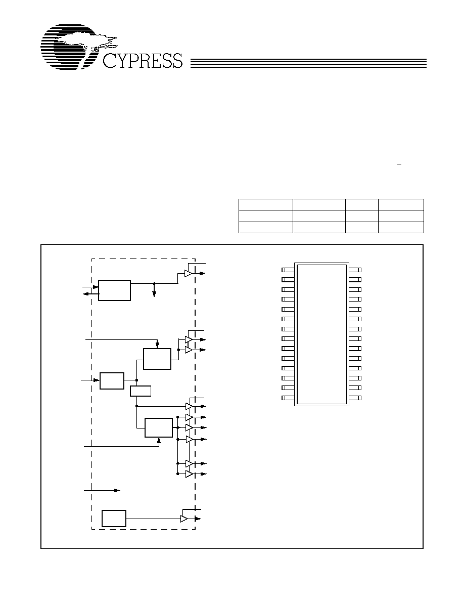
Pin Configuration
Block Diagram
GND
VDDQ3
REF
VDDQ2
CPU0
CPU1
GND
VDDQ3
GND
PCI_STOP#
CPU_STOP#
PWR_DWN#
48MHz
SEL100/66#
28
27
26
25
24
23
22
21
20
19
18
17
16
15
X1
X2
GND
PCI_F
PCI1
VDDQ3
PCI2
PCI3
VDDQ3
PCI4
PCI5
GND
VDDQ3
GND
1
2
3
4
5
6
7
8
9
10
11
12
13
14
VDDQ3
REF
CPU0
CPU1
PCI_F
XTAL
PLL Ref Freq
PLL 1
SEL100/66#
X2
X1
VDDQ3
Stop
Signal
Control
Stop
Signal
Control
PCI1
PWR_DWN#
Power
Down
Control
PCI2
PCI3
PCI4
PCI5
˜2/˜3
OSC
VDDQ2
PCI_STOP#
CPU_STOP#
PLL 2
48MHz
VDDQ3
W48C111-17
PRELIMINARY
2
Pin Definitions
Pin Name
Pin
No.
Pin
Type
Pin Description
CPU0:1
24, 23
O
CPU Clock Outputs 0 and 1: These two CPU clock outputs are controlled by the
CPU_STOP# control pin. Output voltage swing is controlled by voltage applied to
VDDQ2. Frequency of signals is set by SEL100/66# input.
PCI1:5
5, 7, 8, 10,
11
O
PCI Bus Clock Outputs 1 through 5: These five PCI clock outputs are controlled
by the PCI_STOP# control pin. Output voltage swing is controlled by voltage applied
to VDDQ3.
PCI_F
4
O
Fixed PCI Clock Output: Unlike PCI1:5 outputs, this output is not controlled by the
PCI_STOP# control pin; it cannot be forced LOW by PCI_STOP#. Output voltage
swing is controlled by voltage applied to VDDQ3.
48MHz
16
O
48-MHz Output: Fixed clock output at 48 MHz. Output voltage swing is controlled by
voltage applied to VDDQ3.
CPU_STOP#
18
I
CPU_STOP# Input: When brought LOW, clock outputs CPU0:1 are stopped LOW
after completing a full clock cycle (2≠3 CPU clock latency). When brought HIGH,
clock outputs CPU0:1 start with a full clock cycle (2≠3 CPU clock latency).
PCI_STOP#
19
I
PCI_STOP# Input: The PCI_STOP# input enables the PCI1:5 outputs when HIGH
and causes them to remain at logic 0 when LOW. The PCI_STOP signal is latched
on the rising edge of PCI_F. Its effect takes place on the next PCI_F clock cycle.
REF
26
O
Fixed 14.318-MHz Output: Used for various system applications. Output voltage
swing is controlled by voltage applied to VDDQ3.
SEL100/66# 15
I
Frequency Selection Inputs: Select power-up default CPU clock frequency as
shown in Table 1 on page 1.
X1
1
I
Crystal Connection or External Reference Frequency Input: This pin can either
be used as a connection to a crystal or to a reference signal.
X2
2
I
Crystal Connection: An input connection for an external 14.318-MHz crystal. If
using an external reference, this pin must be left unconnected.
PWR_DWN#
17
I
Power-Down Control: When this input is LOW, device goes into a low-power stand-
by condition. All outputs are held LOW. CPU and PCI clock outputs are stopped LOW
after completing a full clock cycle (2≠3 CPU clock cycle latency). When brought
HIGH, CPU and PCI outputs start with a full clock cycle at full operating frequency
(3 ms maximum latency).
VDDQ3
6, 9, 13, 21,
27
P
Power Connection: Connected to 3.3V supply.
VDDQ2
25
P
Power Connection: Power supply for CPU0:1 output buffer. Connected to 2.5V.
GND
3, 12, 14, 20,
22, 28
G
Ground Connection: Connect all ground pins to the common system ground plane.

W48C111-17
PRELIMINARY
3
Spread Spectrum Feature
The device generates a clock that is frequency modulated in
order to increase the bandwidth that it occupies. By increasing
the bandwidth of the fundamental and its harmonics, the am-
plitudes of the radiated electromagnetic emissions are re-
duced. This effect is depicted in Figure 1.
As shown in Figure 1, a harmonic of a modulated clock has a
much lower amplitude than that of an unmodulated signal. The
reduction in amplitude is dependent on the harmonic number
and the frequency deviation or spread. The equation for the
reduction is:
dB = 6.5 + 9*log
10
(P) + 9*log
10
(F)
Where P is the percentage of deviation and F is the frequency
in MHz where the reduction is measured.
The output clock is modulated with a waveform depicted in
Figure 2. This waveform, as discussed in "Spread Spectrum
Clock Generation for the Reduction of Radiated Emissions" by
Bush, Fessler, and Hardin produces the maximum reduction
in the amplitude of radiated electromagnetic emissions. The
deviation selected for this chip is ≠0.5% of the center frequen-
cy. Figure 2 details the Cypress spreading pattern. Cypress
does offer options with more spread and greater EMI reduc-
tion. Contact your local Sales representative for details on
these devices.
Spread
Spectrum
Enabled
EM I R eduction
S pread
S pectrum
N on-
Figure 1. Typical Clock and SSFTG Comparison
MAX (+0.5%)
MIN (≠0.5%)
10%
20%
30%
40%
50%
60%
70%
80%
90%
100%
10%
20%
30%
40%
50%
60%
70%
80%
90%
100%
FREQUENCY
Figure 2. Typical Modulation Profile
W48C111-17
PRELIMINARY
4
Absolute Maximum Ratings
Stresses greater than those listed in this table may cause per-
manent damage to the device. These represent a stress rating
only. Operation of the device at these or any other conditions
above those specified in the operating sections of this specifi-
cation is not implied. Maximum conditions for extended peri-
ods may affect reliability.
Parameter
Description
Rating
Unit
V
DD
, V
IN
Voltage on any pin with respect to GND
≠0.5 to +7.0
V
T
STG
Storage Temperature
≠65 to +150
∞C
T
A
Operating Temperature
0 to +70
∞C
T
B
Ambient Temperature under Bias
≠55 to +125
∞C
ESD
PROT
Input ESD Protection
2 (min.)
kV
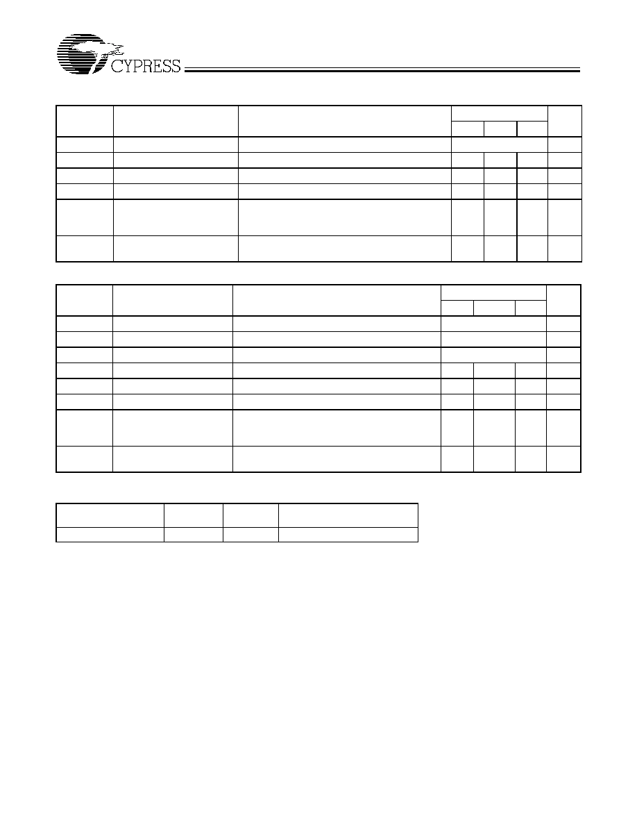
DC Electrical Characteristics:
T
A
= 0∞C to +70∞C, V
DDQ3
= 3.3V±5%, V
DDQ2
= 2.5V±5%, CPU0:1 = 66.6/100 MHz
Parameter
Description
Test Condition
Min.
Typ.
Max.
Unit
Supply Current
I
DD
3.3V Supply Current
Outputs Loaded
[1]
75
mA
I
DD
2.5
2.5V Supply Current
Outputs Loaded
[1]
50
mA
Logic Inputs
V
IL
Input Low Voltage
GND ≠ 0.3
0.8
V
V
IH
Input High Voltage
2.0
V
DD
+ 0.3
V
I
IL
Input Low Current
[2]
≠25
µA
I
IH
Input High Current
[2]
10
µA
I
IL
Input Low Current (SEL100/66#)
≠5
µA
I
IH
Input High Current (SEL100/66#)
5
µA
Clock Outputs
V
OL
Output Low Voltage
I
OL
= 1 mA
50
mV
V
OH
Output High Voltage
I
OH
= ≠1 mA
3.1
V
V
OH
Output High Voltage
CPU0:1
I
OH
= ≠1 mA
2.2
V
I
OL
Output Low Current
CPU0:1
V
OL
= 1.25V
55
115
190
mA
PCI1:5, _F
V
OL
= 1.5V
20.5
53
139
mA
REF
V
OL
= 1.5V
25
37
76
mA
I
OH
Output High Current
CPU0:1
V
OL
= 1.25V
50
110
195
mA
PCI1:5, _F
V
OL
= 1.5V
31
55
189
mA
REFX
V
OL
= 1.5V
27
44
94
mA
Crystal Oscillator
V
TH
X1 Input Threshold Voltage
[3]
V
DDQ3
= 3.3V
1.65
V
C
LOAD
Load Capacitance, as seen by External Crystal
[4]
14
pF
C
IN,X1
X1 Input Capacitance
[5]
Pin X2 unconnected
28
pF
Pin Capacitance/Inductance
C
IN
Input Pin Capacitance
Except X1 and X2
5
pF
C
OUT
Output Pin Capacitance
6
pF
L
IN
Input Pin Inductance
7
nH
Notes:
1.
All clock outputs loaded with 6" 60
transmission lines with 20-pF capacitors.
2.
CPU_STOP#, PCI_STOP#, and PWRDWN# logic inputs have internal pull-up resistors.
3.
X1 input threshold voltage (typical) is V
DD
/2.
4.
The W48C111-17 contains an internal crystal load capacitor between pin X1 and ground and another between pin X2 and ground. Total load placed on crystal
is 14 pF; this includes typical stray capacitance of short PCB traces to crystal.
5.
X1 input capacitance is applicable when driving X1 with an external clock source (X2 is left unconnected).
W48C111-17
PRELIMINARY
5
AC Electrical Characteristics
T
A
= 0∞C to +70∞C, V
DDQ3
= 3.3V±5%,V
DDQ2
= 2.5V± 5%, f
XTL
= 14.31818 MHz
AC clock parameters are tested and guaranteed over stated operating conditions using the stated lump capacitive load at the
clock output.
CPU Clock Outputs, CPU0:1 (Lump Capacitance Test Load = 20 pF)
Parameter
Description
Test Condition/Comments
CPU = 66.6 MHz
CPU = 100 MHz
Unit
Min.
Typ. Max.
Min.
Typ.
Max.
t
P
Period
Measured on rising edge at 1.25V
15
15.5
10
10.5
ns
t
H
High Time
Duration of clock cycle above 2.0V
5.2
3.0
ns
t
L
Low Time
Duration of clock cycle below 0.4V
5.0
2.8
ns
t
R
Output Rise Edge Rate Measured from 0.4V to 2.0V
1
4
1
4
V/ns
t
F
Output Fall Edge Time
Measured from 2.0V to 0.4V
1
4
1
4
V/ns
t
D
Duty Cycle
Measured on rising and falling edge at
1.25V
45
55
45
55
%
t
JC
Jitter, Cycle-to-Cycle
Measured on rising edge at 1.25V. Max-
imum difference of cycle time between
two adjacent cycles.
200
250
ps
t
SK
Output Skew
Measured on rising edge at 1.25V
175
175
ps
f
ST
Frequency Stabiliza-
tion from Power-up
(cold start)
Assumes full supply voltage reached
within 1 ms from power-up. Short cycles
exist prior to frequency stabilization.
3
3
ms
Z
o
AC Output Impedance
Average value during switching transi-
tion. Used for determining series termi-
nation value.
13.5
13.5
PCI Clock Outputs, PCI1:5 and PCI_F (Lump Capacitance Test Load = 30 pF
Parameter
Description
Test Condition/Comments
CPU = 66.6/100 MHz
Unit
Min.
Typ.
Max.
t
P
Period
Measured on rising edge at 1.5V
30
ns
t
H
High Time
Duration of clock cycle above 2.4V
12
ns
t
L
Low Time
Duration of clock cycle below 0.4V
12
ns
t
R
Output Rise Edge Rate
Measured from 0.4V to 2.4V
1
4
V/ns
t
F
Output Fall Edge Rate
Measured from 2.4V to 0.4V
1
4
V/ns
t
D
Duty Cycle
Measured on rising and falling edge at 1.5V
45
55
%
t
JC
Jitter, Cycle-to-Cycle
Measured on rising edge at 1.5V. Maximum
difference of cycle time between two adjacent cycles.
250
ps
t
SK
Output Skew
Measured on rising edge at 1.5V
500
ps
t
O
CPU to PCI Clock Skew
Covers all CPU/PCI outputs. Measured on rising
edge at 1.5V. CPU leads PCI output.
1.5
4
ns
f
ST
Frequency Stabilization
from Power-up (cold
start)
Assumes full supply voltage reached within 1 ms
from power-up. Short cycles exist prior to frequency
stabilization.
3
ms
Z
o
AC Output Impedance
Average value during switching transition. Used for
determining series termination value.
30
W48C111-17
PRELIMINARY
6
Document #:38-00843
REF Clock Output (Lump Capacitance Test Load = 20 pF)
Parameter
Description
Test Condition/Comments
CPU = 66.6/100 MHz
Unit
Min.
Typ.
Max.
f
Frequency, Actual
Frequency generated by crystal oscillator
14.318
MHz
t
R
Output Rise Edge Rate
Measured from 0.4V to 2.4V
0.5
2
V/ns
t
F
Output Fall Edge Rate
Measured from 2.4V to 0.4V
0.5
2
V/ns
t
D
Duty Cycle
Measured on rising and falling edge at 1.5V
45
55
%
f
ST
Frequency Stabilization from
Power-up (cold start)
Assumes full supply voltage reached within 1 ms
from power-up. Short cycles exist prior to
frequency stabilization.
3
ms
Z
o
AC Output Impedance
Average value during switching transition. Used for
determining series termination value.
40
48-MHz Clock Output (Lump Capacitance Test Load = 20 pF)
Parameter
Description
Test Condition/Comments
CPU = 66.6/100 MHz
Unit
Min.
Typ.
Max.
f
Frequency, Actual
Determined by PLL divider ratio (see m/n below)
48.008
MHz
f
D
Deviation from 48 MHz
(48.008 ≠ 48)/48
+167
ppm
m/n
PLL Ratio
(14.31818 MHz x 57/17 = 48.008 MHz)
57/17
t
R
Output Rise Edge Rate
Measured from 0.4V to 2.4V
0.5
2
V/ns
t
F
Output Fall Edge Rate
Measured from 2.4V to 0.4V
0.5
2
V/ns
t
D
Duty Cycle
Measured on rising and falling edge at 1.5V
45
55
%
f
ST
Frequency Stabilization
from Power-up (cold start)
Assumes full supply voltage reached within 1 ms
from power-up. Short cycles exist prior to fre-
quency stabilization.
3
ms
Z
o
AC Output Impedance
Average value during switching transition. Used
for determining series termination value.
40
Ordering Information
Ordering Code
Freq. Mask
Code
Package
Name
Package Type
W48C111
-17
H
28-pin SSOP (209 mils)
W48C111-17
PRELIMINARY
© Cypress Semiconductor Corporation, 1999. The information contained herein is subject to change without notice. Cypress Semiconductor Corporation assumes no responsibility for the use
of any circuitry other than circuitry embodied in a Cypress Semiconductor product. Nor does it convey or imply any license under patent or other rights. Cypress Semiconductor does not authorize
its products for use as critical components in life-support systems where a malfunction or failure may reasonably be expected to result in significant injury to the user. The inclusion of Cypress
Semiconductor products in life-support systems application implies that the manufacturer assumes all risk of such use and in doing so indemnifies Cypress Semiconductor against all charges.
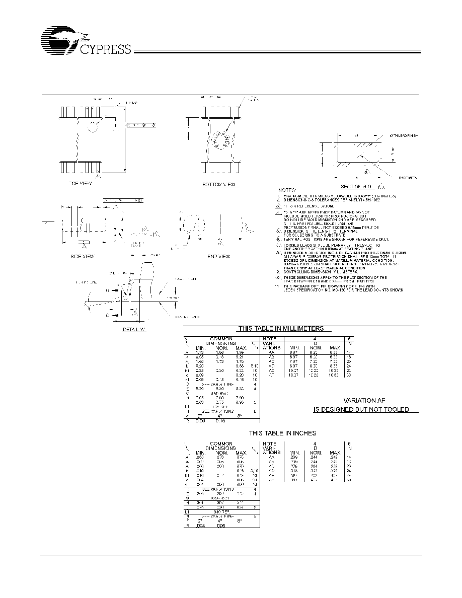
Package Diagram
28-Pin Small Shrink Outline Package (SSOP, 209 mils)