 | –≠–ª–µ–∫—Ç—Ä–æ–Ω–Ω—ã–π –∫–æ–º–ø–æ–Ω–µ–Ω—Ç: BAT54SS3 | –°–∫–∞—á–∞—Ç—å:  PDF PDF  ZIP ZIP |
CYStech Electronics Corp.
Spec. No. : C302S3-H
Issued Date : 2004.04.13
Revised Date :
Page No. : 1/4
BAT54S3/BAT54AS3/BAT54CS3/BAT54SS3
CYStek Product Specification
Small Signal Schottky (double) diodes
BAT54S3/BAT54AS3
BAT54CS3/BAT54SS3
Description
Planar silicon Schottky barrier diodes encapsulated in a SOT-323 very small plastic SMD package.
Single diodes and double diodes with different pinning are available.
Features
∑
Guard ring protected
∑
Low forward voltage drop
∑
Very small plastic SMD package
Applications
∑
Ultra high-speed switching
∑
Voltage clamping
∑
Protection circuits
∑
Blocking diodes
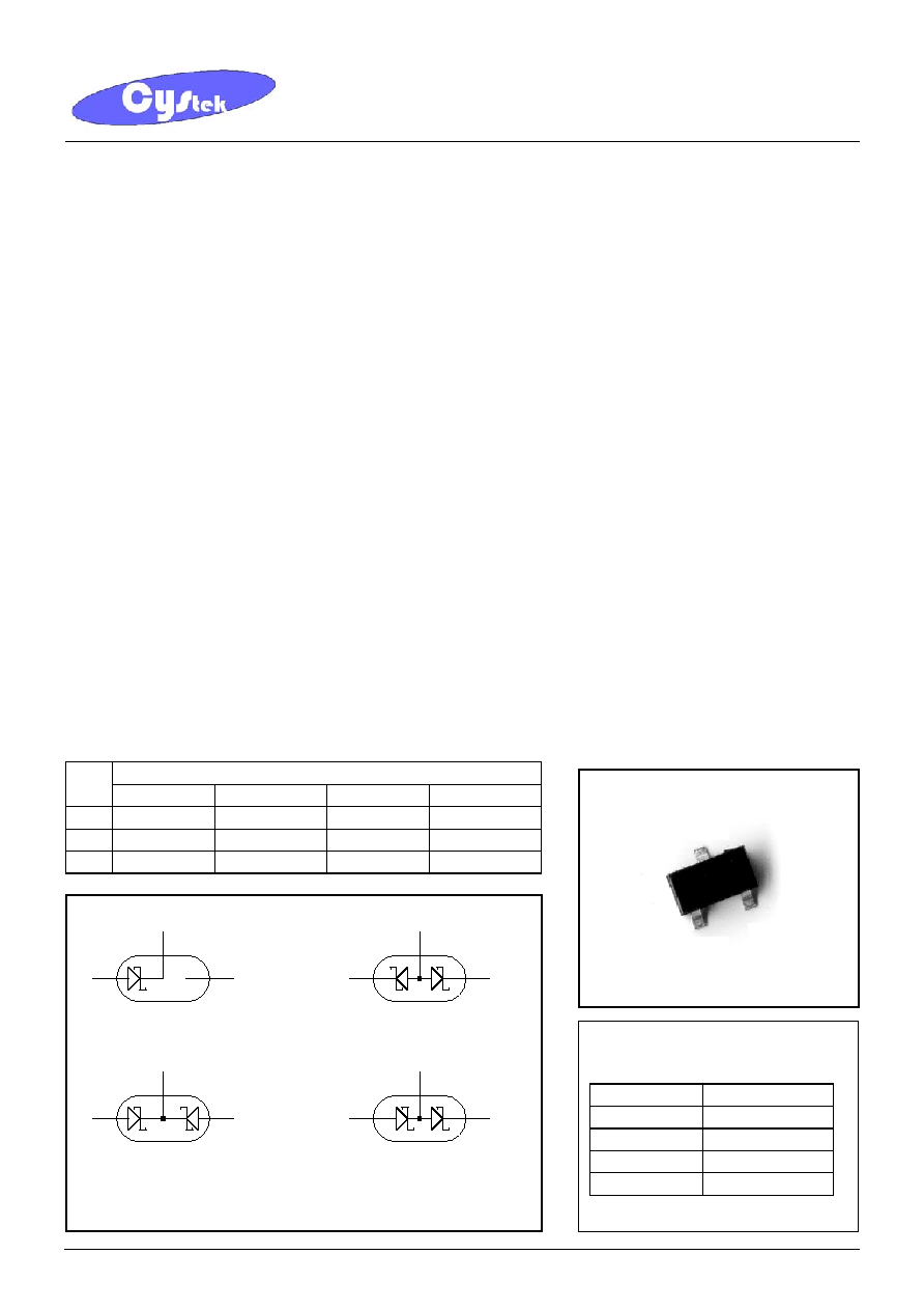
Pinning Outline
Description
Pin
BAT54 BAT54A BAT54C BAT54S
1
A K1 A1 A1
2
NC K2 A2 K2
3 K A1,A2 K1,K2 K1,A1
2
3
1
N.C.
1
2
3
1
2
3
3
2
1
SOT-323
1
2
3
(1) BAT54
(3)BAT54C
(2)BAT54A
(4)BAT54S
Diode configuration and symbol
Marking:
Type Marking
Code
BAT54 S3
L4
BAT54AS3 42
BAT54CS3 43
BAT54SS3 44

CYStech Electronics Corp.
Spec. No. : C302S3-H
Issued Date : 2004.04.13
Revised Date :
Page No. : 2/4
BAT54S3/BAT54AS3/BAT54CS3/BAT54SS3
CYStek Product Specification
Absolute Maximum Ratings
Symbol Parameter
Conditions
Min Max Unit
Per diode
V
R
continuous reverse voltage
-
30
V
I
F
continuous forward current
-
200
mA
I
FRM
repetitive peak forward current
tp1s, 0.5 -
300
mA
I
FSM
non-repetitive peak forward current
tp<10ms
-
600
mA
Ptot
total power dissipation (per package)
Tamb25
- 200
mW
Tstg storage
temperature
-65
+150
Tj junction
temperature
-
125
Tamb
operating ambient temperature
-65
+125
Characteristics
(Ta=25
∞
C, unless otherwise specified)
Parameter Symbol Condition
Min.
Max.
Unit
Reverse Breakdown Voltage
V
BR
I
R
=100µA 30
-
V
V
F
(1) I
F
=0.1mA -
240
mV
V
F
(2) I
F
=1mA -
320
mV
V
F
(3) I
F
=10mA -
400
mV
V
F
(4) I
F
=30mA -
500
mV
Forward Voltage (Note 1)
V
F
(5) I
F
=100mA -
800
mV
Reverse Leakage Current (Note 2)
I
R
V
R
=25V
-
2
µA
Diode Capacitance
C
D
V
R
=1V, f=1MHz
-
10
pF
Reverse Recovery Time
trr
when switched from I
F
= 10mA
to I
R
=10mA; R
L
=100
;
measured at I
R
=1mA
- 5 ns
Notes
:
1.pulse test, tp=380µs, duty cycle<2%.
2.pulse test, tp=300µs, duty cycle<2%.
Thermal Characteristics
Symbol Parameter
Conditions
Value Unit
R
th j-a
thermal resistance from junction to ambient
note 1
625
K/W
Note 1 : Refer to SOT-323 standard mounting conditions.

CYStech Electronics Corp.
Spec. No. : C302S3-H
Issued Date : 2004.04.13
Revised Date :
Page No. : 3/4
BAT54S3/BAT54AS3/BAT54CS3/BAT54SS3
CYStek Product Specification
Characteristic Curves
Forward Current & Forward Voltage
0
50
100
150
200
250
0
200
400
600
800
1000
Forward Voltage-V
F
(mV)
F
o
r
w
ar
d C
u
r
r
en
t
-
I
F
(mA
)
Diode Capacitance & Reverse-Biased Voltage
1
10
100
0.1
1
10
100
Reverse Biased Voltage-V
R
(V)
D
i
ode C
apac
it
anc
e-
C
d
(
p
F
)

CYStech Electronics Corp.
Spec. No. : C302S3-H
Issued Date : 2004.04.13
Revised Date :
Page No. : 4/4
BAT54S3/BAT54AS3/BAT54CS3/BAT54SS3
CYStek Product Specification
SOT-323 Dimension
∑
BAT54 S3 : Single Diode (Marking Code L4)
∑
BAT54AS3 : Common Anode. (Marking Code 42)
∑
BAT54CS3 : Common Cathode. (Marking Code 43)
∑
BAT54SS3 : Series Connected. (Marking Code 44)
*: Typical
Inches Millimeters
Inches Millimeters
DIM
Min. Max. Min. Max.
DIM
Min. Max. Min. Max.
A
0.0315
0.0433
0.80
1.10
e1
0.0256 - 0.65 -
A1 0.0000 0.0039 0.00 0.10 He 0.0787 0.0886 2.00 2.25
bp 0.0118 0.0157 0.30 0.40 Lp 0.0059
0.0177 0.15 0.45
C 0.0039
0.0098 0.10 0.25 Q 0.0051 0.0091 0.13 0.23
D 0.0709
0.0866 1.80 2.20 v 0.0079 -
0.2
-
E 0.0453
0.0531 1.15 1.35 w 0.0079 -
0.2
-
e 0.0512 -
1.3
-
- -
10
∞
0
∞
Notes:
1.Controlling dimension: millimeters.
2.Maximum lead thickness includes lead finish thickness, and minimum lead thickness is the minimum thickness of base material.
3.If there is any question with packing specification or packing method, please contact your local CYStek sales office.
Material:
∑
Lead: 42 Alloy; solder plating
∑
Mold Compound: Epoxy resin family, flammability solid burning class: UL94V-0
Important Notice:
∑
All rights are reserved. Reproduction in whole or in part is prohibited without the prior written approval of CYStek.
∑
CYStek reserves the right to make changes to its products without notice.
∑
CYStek semiconductor products are not warranted to be suitable for use in Life-Support Applications, or systems.
∑
CYStek assumes no liability for any consequence of customer product design, infringement of patents, or application assistance.
Marking:
L4_
Diagram:
3-Lead SOT-323 Plastic
Surface Mounted Package.
CYStek Package Code: S3
XX
He
E
A
A1
Q
Lp
e1
e
bp
1
2
3
D
W
B
v
A
Z
detail Z
A
C
0
1
2
scale
mm