 | –≠–ª–µ–∫—Ç—Ä–æ–Ω–Ω—ã–π –∫–æ–º–ø–æ–Ω–µ–Ω—Ç: BTNA13A3 | –°–∫–∞—á–∞—Ç—å:  PDF PDF  ZIP ZIP |
CYStech Electronics Corp.
Spec. No. : C215A3
Issued Date : 2003.03.27
Revised Date :
Page No. : 1/4
BTNA13A3
CYStek Product Specification
Gentral Purpose NPN Epitaxial Planar Transistor
BTNA13A3
Description
∑
The BTNA14A3 is a darlington amplifier transistor
∑
Complementary to BTPA63A3
.
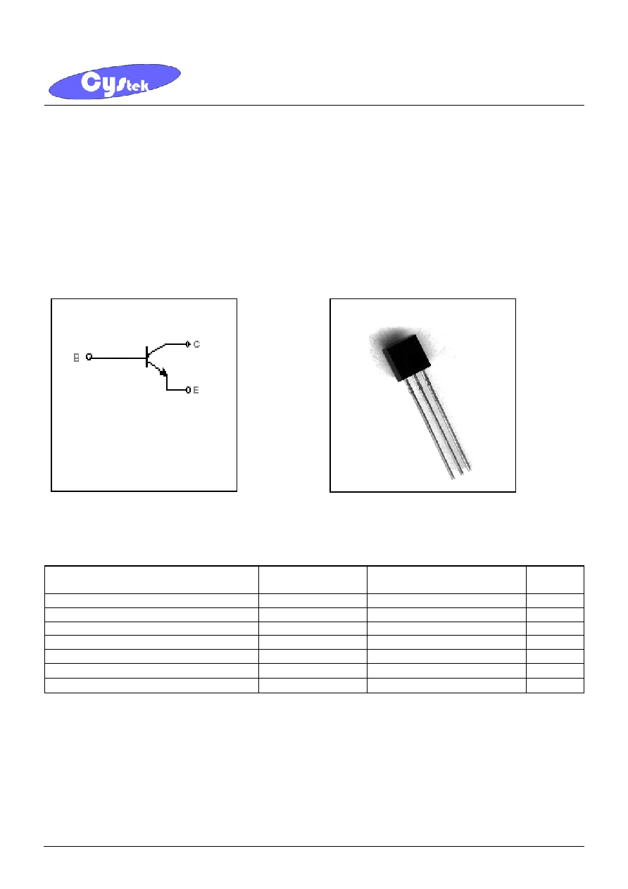
Equivalent Circuit
Absolute Maximum Ratings
(Ta=25
∞
C)
Parameter Symbol
Limits
Unit
Collector-Base Voltage
VCBO
30
V
Collector-Emitter Voltage
VCES
30
V
Emitter-Base Voltage
VEBO
10
V
Collector Current
IC
0.5
A
Power Dissipation
Pd
625
mW
Junction Temperature
Tj
150
∞
C
Storage Temperature
Tstg
-55~+150
∞
C
BTNA13A3
TO-92
BBase
CCollector
EEmitter

CYStech Electronics Corp.
Spec. No. : C215A3
Issued Date : 2003.03.27
Revised Date :
Page No. : 2/4
BTNA13A3
CYStek Product Specification
Characteristics
(Ta=25
∞
C)
Symbol Min.
Typ.
Max.
Unit
Test
Conditions
BVCES 30 -
-
V IC=100uA
ICBO - - 100
nA
VCE=30V
IEBO - - 100
nA
VEB=10V
*VCE(sat) -
- 1.5 V IC=100mA,
IB=0.1mA
*VBE(on) -
- 2.0 V VCE=5V,
IC=100mA
*hFE1 5K -
-
VCE=5V,
IC=10mA
*hFE2 10K -
-
VCE=5V,
IC=100mA
fT
125
-
-
MHz
VCE=5V, IC=10mA, f=100MHz
*Pulse Test: Pulse Width
380us, Duty Cycle
2%
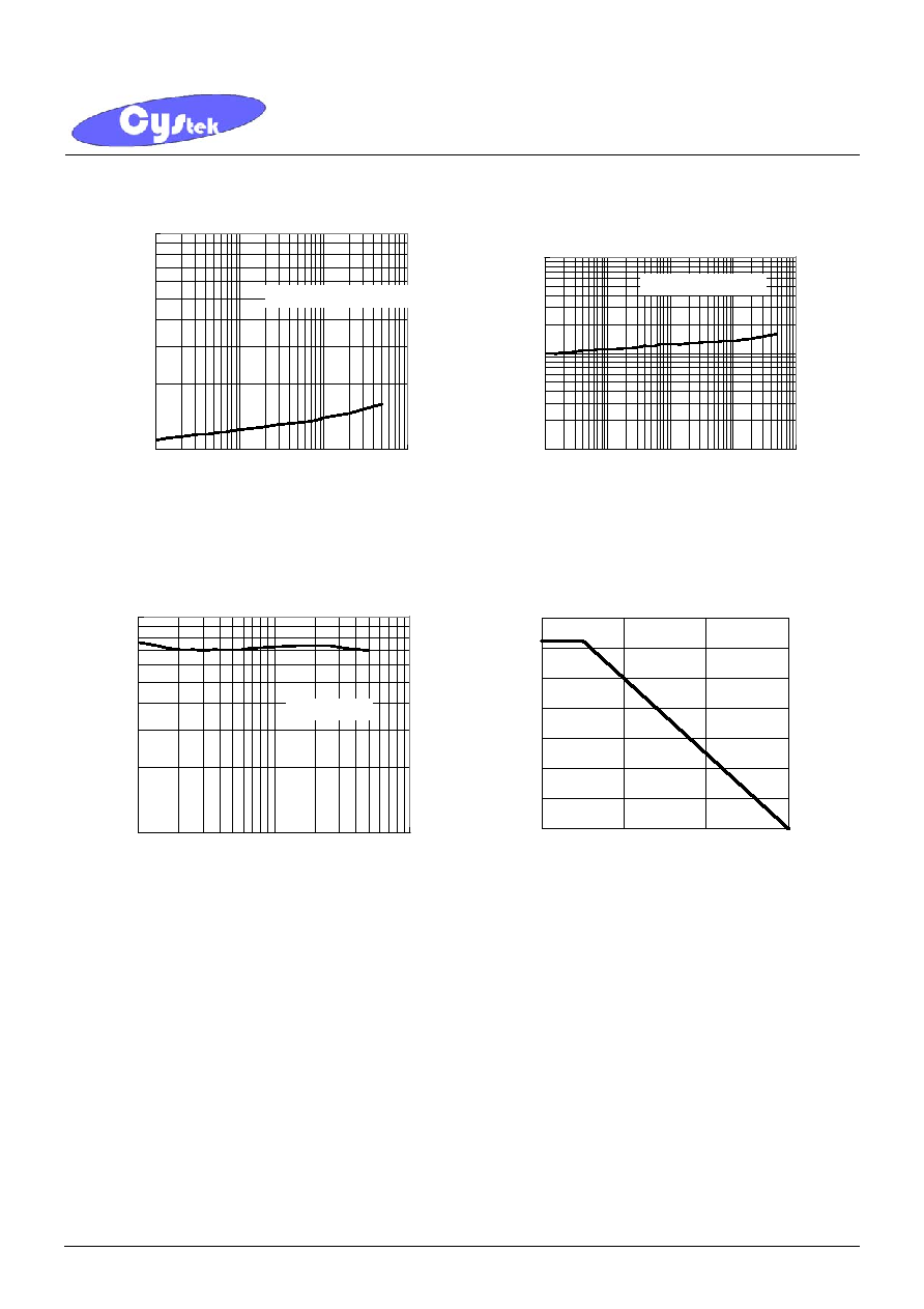
Characteristic Curves
Current Gain vs Collector Current
1000
10000
100000
1
10
100
1000
Collector Current---IC(mA)
Current Gain---
HFE
HFE@VCE=5V
Saturation Voltage vs Collector Current
100
1000
10000
1
10
100
1000
Collector Current ---IC(mA)
Saturation Voltage---(mV)
VCE(SAT)@IC=1000IB
CYStech Electronics Corp.
Spec. No. : C215A3
Issued Date : 2003.03.27
Revised Date :
Page No. : 3/4
BTNA13A3
CYStek Product Specification
Saturation Voltage vs Collector Current
1000
10000
1
10
100
1000
Collector Current ---IC(mA)
Saturation Voltage---(mV)
VBE(SAT)@IC=1000IB
ON Voltage vs Collector Current
100
1000
10000
0.1
1
10
100
1000
Collector Current ---IC(mA)
ON Voltage --- (mV)
VBE(ON)@VCE=5V
Cutoff Frequency vs Collector Current
0.1
1
1
10
100
Collector Current---IC(mA)
Cutoff Frequency---FT(GHZ)
FT@VCE=5V
Power Derating Curve
0
100
200
300
400
500
600
700
0
50
100
150
Ambient Temperature---Ta( )
Power Dissipation--- PD(mW)

cys
tek
CYStech Electronics Corp.
Spec. No. : C214A3
Issued Date : 2003.03.27
Revised Date :
Page No. : 4/4
BTNA14A3
CYStek Product Specification
TO-92 Dimension
*: Typical
Inches Millimeters
Inches Millimeters
DIM
Min. Max. Min. Max.
DIM
Min. Max. Min. Max.
A 0.1704
0.1902 4.33 4.83 G 0.0142 0.0220 0.36 0.56
B 0.1704
0.1902 4.33 4.83 H
-
*
0.1000 -
*
2.54
C 0.5000 - 12.70 -
I
-
*
0.0500 -
*
1.27
D 0.0142
0.0220 0.36 0.56
1
-
*
5
∞
-
*
5
∞
E -
*
0.0500 -
*
1.27
2
-
*
2
∞
-
*
2
∞
F 0.1323
0.1480 3.36 3.76
3
-
*
2
∞
-
*
2
∞
Notes:
1.Controlling dimension: millimeters.
2.Maximum lead thickness includes lead finish thickness, and minimum lead thickness is the minimum thickness of base material.
3.If there is any question with packing specification or packing method, please contact your local CYStek sales office.
Material:
∑
Lead: 42 Alloy ; solder plating
∑
Mold Compound: Epoxy resin family, flammability solid burning class: UL94V-0
Important Notice:
∑
All rights are reserved. Reproduction in whole or in part is prohibited without the prior written approval of CYStek.
∑
CYStek reserves the right to make changes to its products without notice.
∑
CYStek semiconductor products are not warranted to be suitable for use in Life-Support Applications, or systems.
∑
CYStek assumes no liability for any consequence of customer product design, infringement of patents, or application assistance.
A13
Marking:
3
1
A
D
B
C
I
1
E
F
2
3
G
H
2
Style: Pin 1.Emitter 2.Base 3.Collector
3-Lead TO-92 Plastic Package
CYStek Package Code: A3