 | –≠–ª–µ–∫—Ç—Ä–æ–Ω–Ω—ã–π –∫–æ–º–ø–æ–Ω–µ–Ω—Ç: BTNA44A3 | –°–∫–∞—á–∞—Ç—å:  PDF PDF  ZIP ZIP |

CYStech Electronics Corp.
Spec. No. : C211A3
Issued Date : 2003.03.026
Revised Date :2005.03.21
Page No. : 1/5
BTNA44A3
CYStek Product Specification
High Voltage NPN Epitaxial Planar Transistor
BTNA44A3
Features
∑
High breakdown voltage. (BV
CEO
=400V)
∑
Low saturation voltage, typically V
CE
(sat) =60mV at I
C
/I
B=
10mA/1mA.
∑
Complementary to BTPA94A3
Symbol Outline
Absolute Maximum Ratings
(Ta=25
∞
C)
Parameter Symbol
Limit
Unit
Collector-Base Voltage
V
CBO
400
V
Collector-Emitter Voltage
V
CEO
400
V
Emitter-Base Voltage
V
EBO
6
V
Collector Current
I
C
300
mA
Power Dissipation (T
A
=25 )
P
D
0.625
W
Junction Temperature
Tj
150
∞
C
Storage Temperature
Tstg
-55~+150
∞
C
Note : *1. Single Pulse Pw 380
µs,Duty 2%.
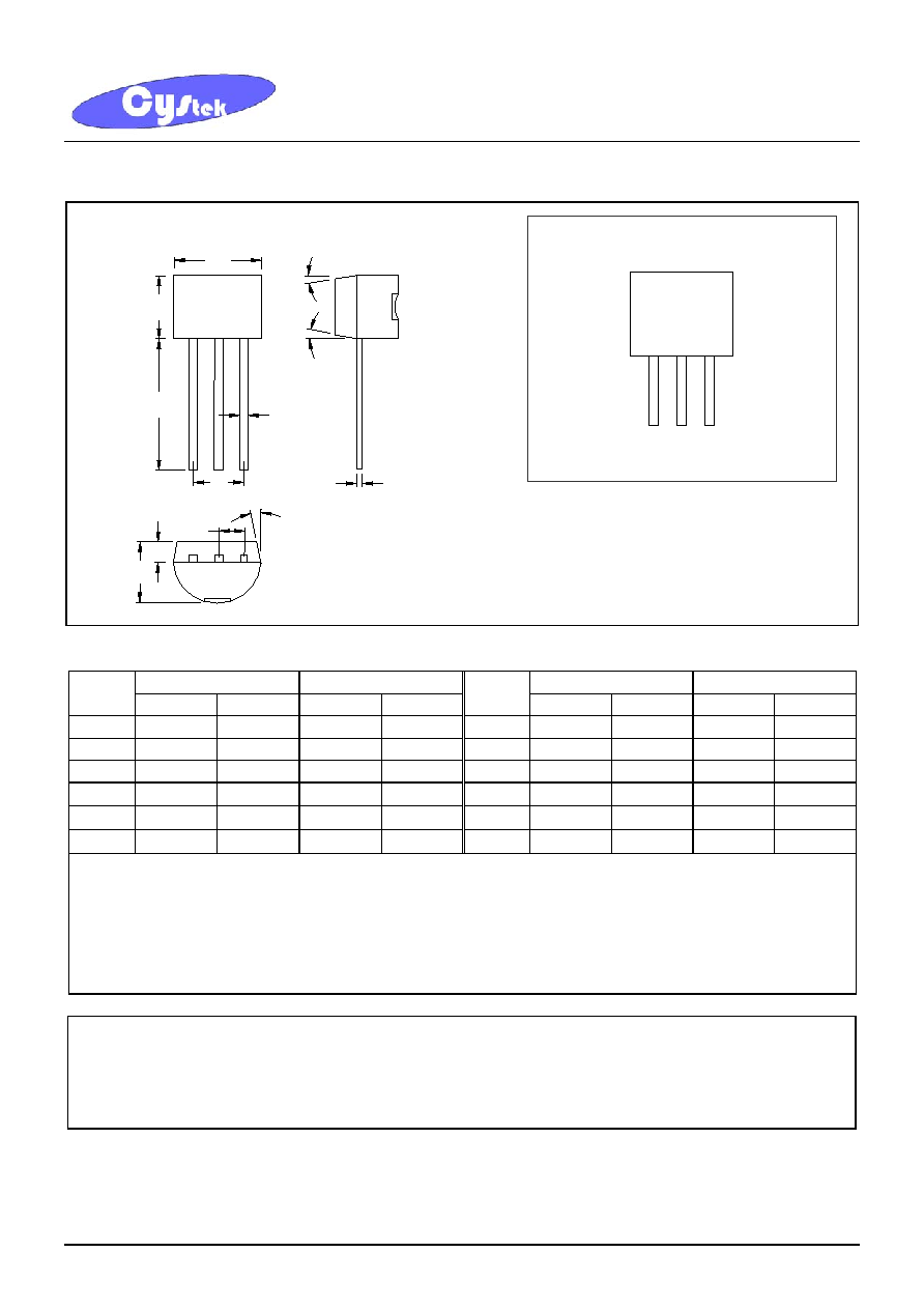
TO-92
BTNA44A3
BBase
CCollector
EEmitter
E B C

CYStech Electronics Corp.
Spec. No. : C211A3
Issued Date : 2003.03.026
Revised Date :2005.03.21
Page No. : 2/5
BTNA44A3
CYStek Product Specification
Characteristics
(Ta=25
∞
C)
Symbol Min. Typ. Max. Unit
Test
Conditions
BV
CBO
400 - - V
I
C
=100µA, I
E
=0
BV
CEO
400 - - V
I
C
=1mA, I
B
=0
BV
EBO
6 - - V
I
E
=10µA, I
C
=0
I
CBO
- -
0.1
µA
V
CB
=400V, I
E
=0
I
EBO
- -
0.1
µA
V
EB
=4V, I
C
=0
I
CES
- -
0.5 µA
V
CE
=400V, V
BE
=0
V
CE(sat)
1
-
0.06
0.35
V
I
C
=1mA, I
B
=0.1mA
V
CE(sat)
2 - 0.06
0.35 V
I
C
=10mA, I
B
=1mA
*V
CE(sat)
3 - 0.1 0.75 V
I
C
=50mA, I
B
=5mA
V
BE(sat)
- 0.68
0.75
V
I
C
=10mA, I
B
=1mA
h
FE
1 40 - - -
V
CE
=10V, I
C
=1mA
h
FE
2 52 - 270 -
V
CE
=10V, I
C
=10mA
*h
FE
3 45 - - -
V
CE
=10V, I
C
=50mA
*h
FE
4 40 - - -
V
CE
=10V, I
C
=100mA
f
T
50
- -
MHz
V
CE
=20V, I
E
=10mA, f=100MHz
Cob - 4 -
pF
V
CB
=20V, f=1MHz
*Pulse Test : Pulse Width
380µs, Duty Cycle
2%
Classification Of h
FE
2
Rank K P
Q
Range 52~120 82~180
120~270

CYStech Electronics Corp.
Spec. No. : C211A3
Issued Date : 2003.03.026
Revised Date :2005.03.21
Page No. : 3/5
BTNA44A3
CYStek Product Specification
Characteristic Curves
Current Gain vs Collector Current
10
100
1000
1
10
100
1000
Collector Current ---IC(mA)
Current Gain---
HFE
VCE=10V
VCE=5V
Saturation Voltage vs Collector Current
10
100
1000
10000
1
10
100
1000
Collector Current ---IC(mA)
Saturation Voltage-(mV)
VCESAT
IC=10IB
IC=20IB
IC=30IB
Saturation Voltage vs Collector Current
100
1000
10000
1
10
100
1000
Collector Current--- IC(mA)
Saturation Voltage-(mV)
VBESAT@IC=10IB
Power Derating Curve
0
100
200
300
400
500
600
700
0
50
100
150
200
Ambient Temperature---TA()
Powe
r Dissipa
tion---PD(mW)

CYStech Electronics Corp.
Spec. No. : C211A3
Issued Date : 2003.03.026
Revised Date :2005.03.21
Page No. : 4/5
BTNA44A3
CYStek Product Specification
TO-92 Taping Outline
Millimeters
DIM Item
Min. Max.
A Component
body
height
4.33
4.83
D Tape
Feed
Diameter
3.80
4.20
D1 Lead
Diameter
0.36
0.53
D2 Component
Body
Diameter
4.33
4.83
F1,F2 Component
Lead
Pitch
2.40
2.90
F1,F2 F1-F2
-
±
0.3
H
Height Of Seating Plane
15.50
16.50
H1
Feed Hole Location
8.50
9.50
H2
Front To Rear Deflection
-
1
H2A
Deflection Left Or Right
-
1
H3 Component
Height
-
27
H4
Feed Hole To Bottom Of Component
-
21
L
Lead Length After Component Removal
-
11
L1
Lead Wire Enclosure
2.50
-
P
Feed Hole Pitch
12.50
12.90
P1
Center Of Seating Plane Location
5.95
6.75
P2
4 Feed Hole Pitch
50.30
51.30
T
Over All Tape Thickness
-
0.55
T1
Total Taped Package Thickness
-
1.42
T2
Carrier Tape Thickness
0.36
0.68
W Tape
Width
17.50
19.00
W1 Adhesive
Tape
Width
5.00
7.00
-
20 pcs Pitch
253
255
H2A
H2A
H2
H2
D2
A
H
W
W1
H3
H4
H1
L1
L
P2
P
P1
F1F2
D1
D
T2
T
T1
CYStech Electronics Corp.
Spec. No. : C211A3
Issued Date : 2003.03.026
Revised Date :2005.03.21
Page No. : 5/5
BTNA44A3
CYStek Product Specification
TO-92 Dimension
*: Typical
Inches Millimeters
Inches Millimeters
DIM
Min. Max. Min. Max.
DIM
Min. Max. Min. Max.
A 0.1704
0.1902 4.33 4.83 G 0.0142
0.0220 0.36 0.56
B 0.1704
0.1902 4.33 4.83 H
-
*
0.1000 -
*
2.54
C 0.5000 - 12.70 -
I
-
*
0.0500 -
*
1.27
D 0.0142
0.0220 0.36 0.56
1
-
*
5
∞
-
*
5
∞
E -
*
0.0500 -
*
1.27
2
-
*
2
∞
-
*
2
∞
F 0.1323
0.1480 3.36 3.76
3
-
*
2
∞
-
*
2
∞
Notes:
1.Controlling dimension: millimeters.
2.Maximum lead thickness includes lead finish thickness, and minimum lead thickness is the minimum thickness of base material.
3.If there is any question with packing specification or packing method, please contact your local CYStek sales office.
Material:
∑
Lead: 42 Alloy ; solder plating
∑
Mold Compound: Epoxy resin family, flammability solid burning class: UL94V-0
Important Notice:
∑
All rights are reserved. Reproduction in whole or in part is prohibited without the prior written approval of CYStek.
∑
CYStek reserves the right to make changes to its products without notice.
∑
CYStek semiconductor products are not warranted to be suitable for use in Life-Support Applications, or systems.
∑
CYStek assumes no liability for any consequence of customer product design, infringement of patents, or application assistance.
3
1
A
D
B
C
I
1
E
F
2
3
G
H
2
Marking:
NA44
1
3
2
Style: Pin 1.Emitter 2.Base 3.Collector
3-Lead TO-92 Plastic Package
CYStek Package Code: A3