 | –≠–ª–µ–∫—Ç—Ä–æ–Ω–Ω—ã–π –∫–æ–º–ø–æ–Ω–µ–Ω—Ç: CMBD914N3 | –°–∫–∞—á–∞—Ç—å:  PDF PDF  ZIP ZIP |
CYStech Electronics Corp.
Spec. No. : C303N3
Issued Date : 2003.04.12
Revised Date
Page No. : 1/4
CMBD914N3
CYStek Product Specification
High ≠speed switching diode
CMBD914N3
Description
The CMBD914N3 is a high-speed switching diode fabricated in planar technology, and encapsulated in
the small SOT-23 plastic SMD package.
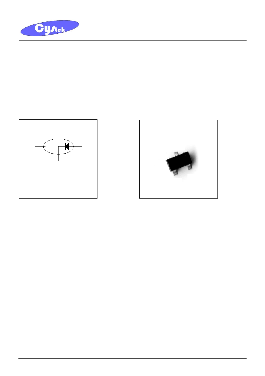
Equivalent Circuit
Features
∑
Small plastic SMD package
∑
High switching speed: max. 4ns
∑
Continuous reverse voltage: max. 70V
∑
Repetitive peak reverse voltage: max. 85V
∑
Repetitive peak forward current: max. 500mA.
Applications
∑
High-speed switching in thick and thin-film circuits.
SOT-23
CMBD914N3
1Anode
2Not Connected
3Cathode
Anode
NC
Cathode
1
2
3

CYStech Electronics Corp.
Spec. No. : C303N3
Issued Date : 2003.04.12
Revised Date
Page No. : 2/4
CMBD914N3
CYStek Product Specification
Absolute Maximum Ratings
@TA=25
Parameters Symbol
Min
Max
Unit
Repetitive peak reverse voltage
V
RRM
- 85
V
Continuous reverse voltage
V
R
- 70
V
Continuous forward current
I
F
-
200
mA
Repetitive peak forward current
I
FRM
500
mA
Non-repetitive peak forward current
@square wave, Tj=125 prior to surge t=1µs
t=1ms
t=1s
I
FSM
-
-
-
4
1
0.5
A
A
A
Total power dissipation(
Note 1
) Ptot
250
mW
Junction Temperature
T
j
-
150
∞
C
Storage Temperature
T
stg
-65
+150
∞
C
Note 1: Device mounted on an FR-4 PCB.
Electrical Characteristics
@ Tj=25 unless otherwise specified
Parameters Symbol Conditions Min
Typ.
Max
Unit
Forward voltage
V
F
I
F
=1mA
I
F
=10mA
I
F
=50mA
I
F
=150mA
- -
715
855
1
1.25
mV
mV
V
V
Reverse current
I
R
V
R
=25V
V
R
=75V
V
R
=25V,Tj=150
V
R
=75V,Tj=150
- -
30
1
30
50
nA
µA
µA
µA
Diode capacitance
Cd
V
R
=0V, f=1MHz
-
-
1.5
pF
Reverse recovery time
trr
when switched from I
F
=10mA to
I
R
=10mA,R
L
=100, measured
at I
R
=1mA
- - 4 ns
Forward recovery voltage
Vfr
when switched from I
F
=10mA
tr=20ns
- -
1.75
V
Thermal Characteristics
Symbol Parameter Conditions
Value
Unit
Rth,j-tp
thermal resistance from junction to tie-point
360
/W
Rth, j-a
thermal resistance from junction to ambient
Note 1
500
/W
Note 1: Device mounted on an FR-4 PCB.

CYStech Electronics Corp.
Spec. No. : C303N3
Issued Date : 2003.04.12
Revised Date
Page No. : 3/4
CMBD914N3
CYStek Product Specification
Characteristic Curves
Forward Biased Voltage & Forward Current
0
150
300
450
0
500
1000
1500
2000
Forward Biased Voltage-VF(mV)
Cu
rr
e
n
t
-I
F
(m
A
)
Capacitance & Reverse-Biased Voltage
0.1
1
0.1
1
10
100
Reverse Biased Voltage-V
R
(V)
Ca
p
a
c
i
t
a
n
c
e
-
Cd
(
p
F
)
Capacitance & Reverse-Biased Voltage
0.1
1
0.1
1
10
100
Reverse Biased Voltage-V
R
(V)
Ca
p
a
c
i
t
a
n
c
e
-
Cd
(
p
F
)
Power Derating
0
50
100
150
200
250
300
0
20
40
60
80
100
120
140
160
Ta(
o
C ), Ambient Temperature
P
D
(m
W
)
, P
o
w
e
r D
i
s
s
i
p
a
ti
o
n
CYStech Electronics Corp.
Spec. No. : C303N3
Issued Date : 2003.04.12
Revised Date
Page No. : 4/4
CMBD914N3
CYStek Product Specification
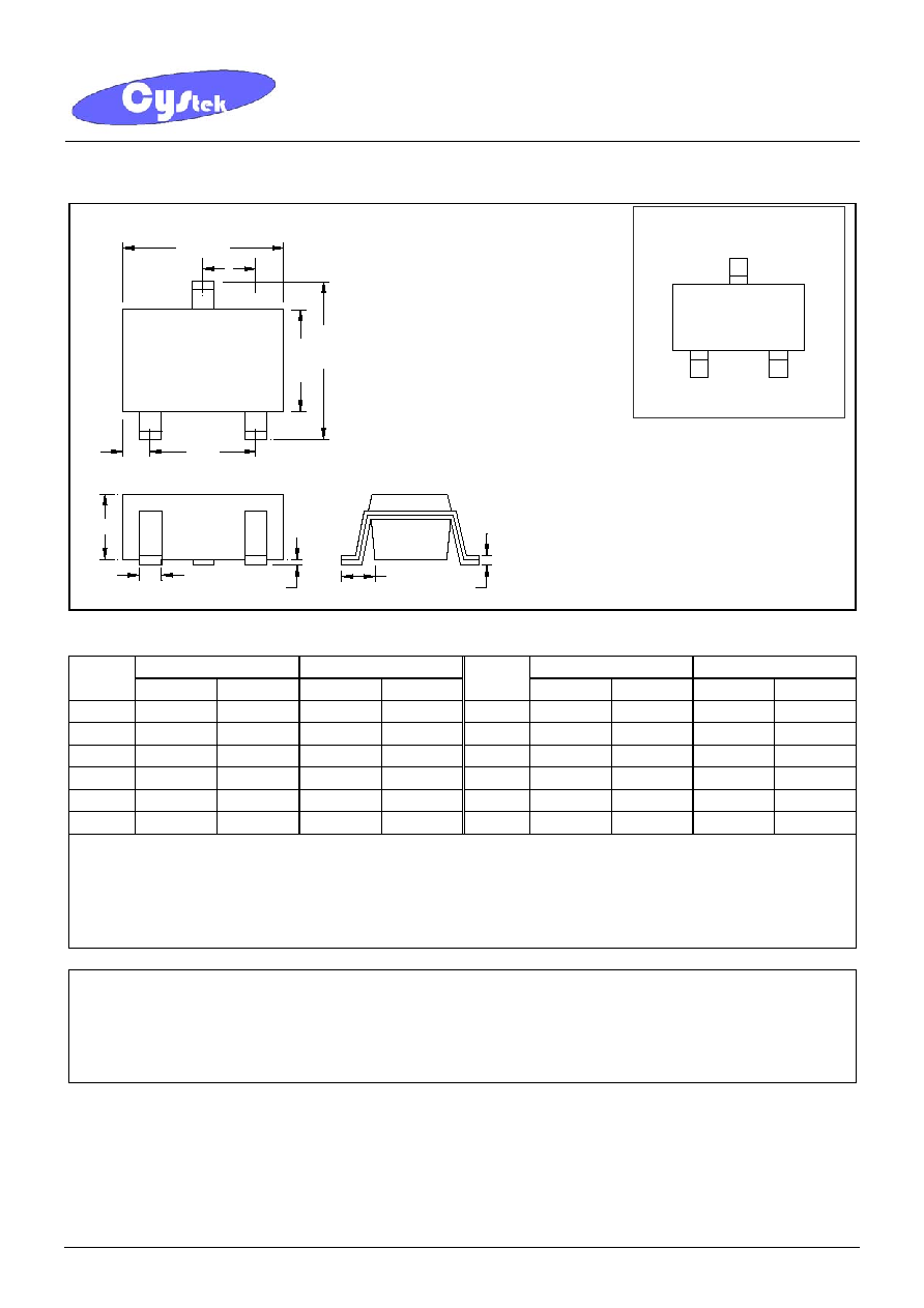
SOT-23 Dimension
*: Typical
Inches Millimeters
Inches Millimeters
DIM
Min. Max. Min. Max.
DIM
Min. Max. Min. Max.
A 0.1102
0.1204 2.80 3.04 J 0.0034
0.0070
0.085 0.177
B 0.0472
0.0630 1.20 1.60 K 0.0128 0.0266 0.32 0.67
C 0.0335
0.0512 0.89 1.30 L 0.0335 0.0453 0.85 1.15
D 0.0118
0.0197 0.30 0.50 S 0.0830
0.1083 2.10 2.75
G 0.0669
0.0910 1.70 2.30 V 0.0098 0.0256 0.25 0.65
H
0.0005
0.0040
0.013
0.10
Notes:
1.Controlling dimension: millimeters.
2.Maximum lead thickness includes lead finish thickness, and minimum lead thickness is the minimum thickness of base material.
3.If there is any question with packing specification or packing method, please contact your local CYStek sales office.
Material:
∑
Lead: 42 Alloy ; solder plating
∑
Mold Compound: Epoxy resin family, flammability solid burning class: UL94V-0
Important Notice:
∑
All rights are reserved. Reproduction in whole or in part is prohibited without the prior written approval of CYStek.
∑
CYStek reserves the right to make changes to its products without notice.
∑
CYStek semiconductor products are not warranted to be suitable for use in Life-Support Applications, or systems.
∑
CYStek assumes no liability for any consequence of customer product design, infringement of patents, or application assistance.
H
J
K
D
A
L
G
V
C
B
3
2
1
S
Style:Pin.1. Anode 2. Not Connected
3.Cathode
Marking:
TE
3-Lead SOT-23 Plastic
Surface Mounted Package
CYStek Package Code: N3
5H