
SBR520 THRU SBR5100
CURRENT 5.0Amperes
VOLTAGE 20 to 100 Volts
Maximum Ratings and Electrical Characteristics
Notes:
(1) Pulse test: 300S pulse width, 1% duty cycle
(2) Thermal resistance from junction to case
(Ratings at 25 ambient temperature unless otherwise specified, single phase, half wave, resistive or inductive
load. For capacitive load, derate by 20%)
Features
Mechanical Data
∑ Plastic Package has Underwriters Laboratory
Flammability Classification 94V-0
∑ Metal silicon junction, majority carrier conduction
∑ Guard ring for overvoltage protection
∑ Low power loss, high efficiency
∑ High current capability, Low forward voltage drop
∑ Single rectifier construction
∑ High surge capability
∑ For use in low voltage, high frequency inverters,
free wheeling, and polarity protection applications
∑ High temperature soldering guaranteed:
250/10 seconds, 0.25" (6.35mm) from case
∑ Case : JEDEC ITO-220A molded plastic body
∑ Terminals : Lead solderable per
MIL-STD-750, Method 2026
∑ Polarity : As marked
∑ Mounting Position : Any
∑ Weight : 0.08 ounce, 2.24 grams
Symbols
SBR
520
SBR
540
Units
Maximum repetitive peak reverse voltage
V
RRM
20
30
40
Volts
Maximum RMS voltage
V
RMS
0.55
0.70
Maximum DC blocking voltage
V
DC
Volts
Maximum average forward rectified current
(see Fig. 1)
I(
AV
)
5.0
Peak forward surge current 8.3ms single half
sine-wave superimposed on rated load
(JEDEC method)
100.0
Amps
Maximum instantaneous forward voltage
at 5.0A (Note 1)
V
F
1.0
Volts
T
A
=25
15
Maximum instantaneous reverse
current at rated DC blocking
voltage (Note1)
T
A
=125
mA
Typical thermal resistance (Note 2)
/W
Operating junction temperature range
-65 to +125
I
R
I
FSM
T
J
Volts
SBR
530
14
21
28
20
30
40
Repetitive peak forward current(square wavr,
20KHZ) at Tc=105
Storage temperature range
T
STG
-65 to +150
-65 to +150
0.85
SBR
560
SBR
590
60
80
90
SBR
580
42
56
63
60
80
90
SBR
5100
100
70
100
R
JC
5.0
50
10.0
Amps
Amps
I
FRM
Dimensions in inches and (millimeters)
ITO-220A
5.08
1
3
M
i
n
3
.
7
0
.
2
0.7 0.2
1.3 0.2
2
.
7
0
.
2
1
5
0
.
3
10 0.5
3.2
6
.
4
0
.
1
2.7
4.5 0.2
0.5
2.4
+
+
PIN 1
PIN 1
PIN 2
PIN 2
CASE
CASE
CasePositive
Case Negative
Suffix"R"
+
+
+
+
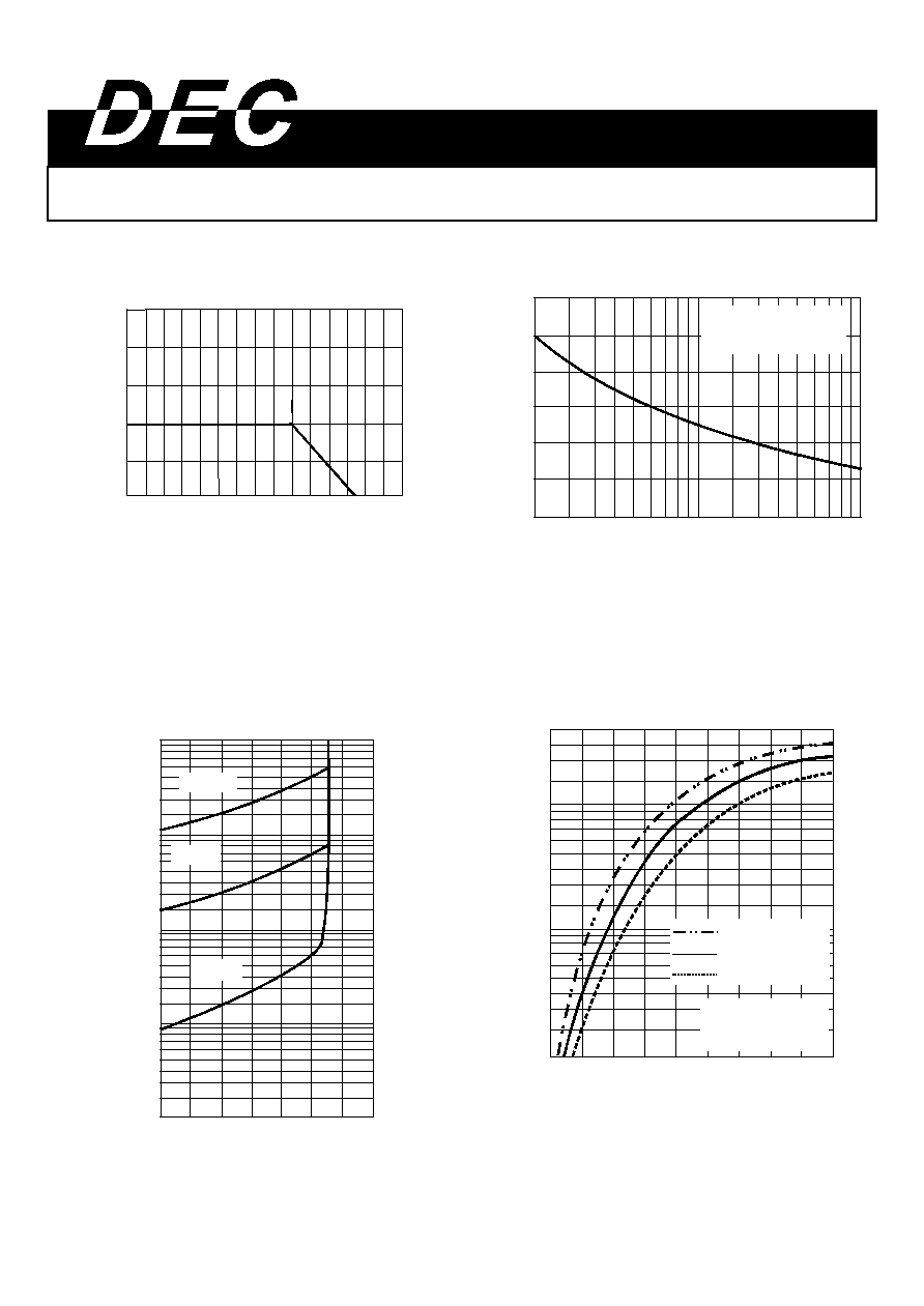
RATINGS AND CHARACTERISTIC CURVES SBR520-SBR5100
FIG. 1 - FORWARD CURRENT DERATING CURVE
12.5
10
7.5
5
2.5
0
A
V
E
R
A
G
E
F
O
R
W
A
R
D
C
H
R
R
E
N
T
.
A
M
P
E
R
E
S
0 50 100 150
CASE TEMPERATURE, !!!!
FIG. 3 - TYPICAL REVERSE
CHARACTERISTICS
100
10
1.0
0.1
0.01
I
N
S
T
A
N
T
A
N
E
O
U
S
R
E
V
E
R
S
E
C
U
R
R
E
N
T
,
M
I
L
L
I
A
M
P
E
R
E
S
0 20 40 60 80 100 120 140
PERAENT OR RATED VOLTAGE PEAK
REVERSE VOLTAGE
FIG. 2 - MAXIMUM NON-REPETITIVE
SURGE CURRENT
150
125
100
75
50
25
0
P
E
A
K
F
O
R
W
A
R
D
S
U
R
G
E
C
U
R
R
E
N
T
,
A
M
P
E
R
E
S
1 2 5 10 20 50 100
NUMBER OF CYCLES AT 60H
Z
T
J
=100
T
J
=75
T
J
=25
FIG. 4 - TYPICAL INSTANTANEOUS
FORWARD CHARACTERISTICS
50
10
1.0
0.1
I
N
S
T
A
N
T
A
N
E
O
U
S
F
O
R
W
A
R
D
C
U
R
R
E
N
T
A
M
P
E
R
E
S
0.2 0.3 0.4 0.5 0.6 0.7 0.8 0.9 1.0
INSTANTANEOUS FORWARD VOLTAGE,
VOLTS
T
J
=25
PULSE WIDTH=300us
2% DUTY CYCLE
T
L
=75
o
C
8.3ms SINGLE HALF SINE-WAVE
JEDEC METHOD
SBR520~540
SBR560~580
SBR590~5100