
SMAJ5.0 THRU SMAJ188CA
Features
Mechanical Data
∑ Plastic package has Underwriters Laboratory
flammability classification 94V-0
∑ Optimized for LAN protection applications
∑ Ideal for ESD protection of data lines in accordance with
IEC 1000-4-2 (IEC801-2)
∑ Ideal for EFT protection of data lines in accordance with
IEC 1000-4-4 (IEC801-4)
∑ Low profile package with built-in strain relief for surface
mounted applications
∑ Glass passivated junction
∑ Low incremental surge resistance, excellent clamping
capability
∑ 400W peak pulse power capability with a 10/1000S
waveform, repetition rate(duty cycle) : 0.01% (300W above 78V)
∑ Very fast response time
∑ High temperature soldering guaranteed : 250/10 seconds
at terminals
Devices For Bidirectional Applications
Maximum Ratings And Electrical Characteristics
∑ For bi-directional devices, use suffix C or CA (e.g. SMAJ10C, SMAJ10CA).
Electrical characteristics apply in both directions.
∑ Case : JEDEC DO-214AC(SMA) molded plastic
over passivated chip
∑ Terminals : Solder plated , solderable per
MIL-STD-750, method 2026
∑ Polarity : For uni-directional types the band denotes
the cathode, which is positive with respect to the
anode under normal TVS operation
∑ Mounting Position : Any
∑ Weight : 0.002 ounce, 0.064 gram
Peak pulse power dissipation with a 10/1000S waveform (Note 1,2. Fig. 1)
Peak pulse current with a waveform (Note 1)
Typical thermal resistance, junction to lead
Typical thermal resistance, junction to ambient (Note 3)
Peak forward surge current, 8.3mm single half sine-wave unidirectional only (Note 2)
Operating junction and storage temperature range
P
PPM
400
Watts
Symbols
Values
Units
30
I
PPM
See next table
Amps
40
I
FSM
T
J
,T
STG
120
-55 to +150
/W
/W
Amps
(Ratings at 25 ambient temperature unless otherwise specified)
Notes:
(1) Non repetitive current pulse, per Fig.3 and derated above T
A
=25 per Fig.2 Rating is 300W above 78V
(2) Mounted on 0.2◊0.2"(5.0◊5.0mm) copper pads to each terminal
(3) Mounted on minimum recommended pad layout
POWER 400Watts
VOLTAGE 5.0 to 188 Volts
Dimensions in inches and (millimeters)
0.058(1.47)
0.052(1.32)
0.110(2.79)
0.100(2.54)
0.012(0.31)
0.006(0.15)
0.177(4.50)
0.157(3.99)
0.090(2.29)
0.078(1.98)
0.060(1.52)
0.030(0.76)
0.005(0.127)
MAX.
0.208(5.28)
0.194(4.93)
DO-214AC (SMA)
R
JA
R
JL

ELECTRICAL CHARACTERISTIC
Ratings at 25 ambient temperature unless otherwise specified. VF=3.5V at IF=25A (uni-directional only)
Device
Breakdown Voltage
Maximum
Maximum
Maximum
Device Type
Marking
V
(BR)
at I
T
(1)
Test
Stand-off
Reverse Leakage Peak Pulse Surge
Clamping
Code
(V)
Current
Voltage
at V
WM
Current I
PPM
Voltage at I
PPM
UNI
BI
Max
Min
I
T
(mA)
V
WM
(V)
I
D
(
A
)
(3)
(A)
(2)
V
C
(V)
S MAJ 5.0
(C )
AD
WD
6.40
7.82
7.07
10
5.0
800
41.7
9.6
S MAJ 5.0
(C )
A
(5)
AE
WE
6.40
10
5.0
800
43.5
9.2
S MAJ 6.0
(C )
AF
WF
6.67
8.15
7.37
10
6.0
800
35.1
11.4
S MAJ 6.0
(C )
A
AG
WG
6.67
10
6.0
800
38.8
10.3
S MAJ 6.5
(C )
AH
WH
7.22
7.22
8.82
10
6.5
500
32.5
12.3
S MAJ 6.5
(C )
A
AK
WK
7.98
10
6.5
500
35.7
11.2
S MAJ 7.0
(C )
AL
WL
7.78
9.51
8.60
10
7.0
200
30.1
13.3
S MAJ 7.0
(C )
A
AM
WM
7.78
10
7.0
200
33.3
12.0
S MAJ 7.5
(C )
AN
WN
8.33
10.2
9.21
1.0
7.5
100
28.0
14.3
S MAJ 7.5
(C )
A
AP
WP
8.33
1.0
7.5
100
31.0
12.9
S MAJ 8.0
(C )
AQ
WQ
8.89
10.9
9.83
1.0
8.0
50
26.7
15.0
S MAJ 8.0
(C )
A
AR
WR
8.89
1.0
8.0
50
29.4
13.6
S MAJ 8.5
(C )
AS
WS
9.44
11.5
10.4
1.0
8.5
10
25.2
15.9
S MAJ 8.5
(C )
A
AT
WT
9.44
1.0
8.5
10
27.8
14.4
S MAJ 9.0
(C )
AU
WU
10.0
12.2
11.1
1.0
9.0
5.0
23.7
16.9
S MAJ 9.0
(C )
A
AV
WV
10.0
1.0
9.0
5.0
26.0
15.4
S MAJ 10
(C )
AW
WW
11.1
13.6
12.3
1.0
10
1.0
21.3
18.8
S MAJ 10
(C )
A
AX
WX
11.1
1.0
10
1.0
23.5
17.0
S MAJ 11
(C )
AY
WY
12.2
14.9
13.5
1.0
11
1.0
19.9
20.1
S MAJ 11
(C )
A
AZ
WZ
12.2
1.0
11
1.0
22.0
18.2
S MAJ 12
(C )
B D
XD
13.3
16.3
14.7
1.0
12
1.0
18.2
22.0
S MAJ 12
(C )
A
B E
XE
13.3
1.0
12
1.0
20.1
19.9
S MAJ 13
(C )
B F
XF
14.4
17.6
15.9
1.0
13
1.0
16.8
23.8
S MAJ 13
(C )
A
B G
XG
14.4
1.0
13
1.0
18.6
21.5
S MAJ 14
(C )
B H
XH
15.6
19.1
17.2
1.0
14
1.0
15.5
25.8
S MAJ 14
(C )
A
B K
XK
15.6
1.0
14
1.0
17.2
23.2
S MAJ 15
(C )
B L
XL
16.7
20.4
18.5
1.0
15
1.0
14.9
26.9
S MAJ 15
(C )
A
B M
XM
16.7
1.0
15
1.0
16.4
24.4
S MAJ 16
(C )
B N
XN
17.8
21.8
19.7
1.0
16
1.0
13.9
28.8
S MAJ 16
(C )
A
B P
XP
17.8
1.0
16
1.0
15.4
26.0
S MAJ 17
(C )
B Q
XQ
18.9
23.1
20.9
1.0
17
1.0
13.1
30.5
S MAJ 17
(C )
A
B R
XR
18.9
1.0
17
1.0
14.5
27.6
S MAJ 18
(C )
B S
XS
20.0
24.4
22.1
1.0
18
1.0
12.4
32.2
S MAJ 18
(C )
A
B T
XT
20.0
1.0
18
1.0
13.7
29.2
S MAJ 20
(C )
B U
XU
22.2
27.1
24.5
1.0
20
1.0
11.2
35.8
S MAJ 20
(C )
A
B V
XV
22.2
1.0
20
1.0
12.3
32.4
S MAJ 22
(C )
B W
XW
24.4
29.8
26.9
1.0
22
1.0
10.2
39.4
S MAJ 22
(C )
A
B X
XX
24.4
1.0
22
1.0
11.3
35.5
S MAJ 24
(C )
B Y
XY
26.7
32.6
29.5
1.0
24
1.0
9.3
43.0
S MAJ 24
(C )
A
B Z
XZ
26.7
1.0
24
1.0
10.3
38.9
S MAJ 26
(C )
C D
Y D
28.9
35.3
31.9
1.0
26
1.0
8.6
46.6
S MAJ 26
(C )
A
C E
Y E
28.9
1.0
26
1.0
9.5
42.1
S MAJ 28
(C )
C F
Y F
31.1
38.0
34.4
1.0
28
1.0
8.0
50.0
S MAJ 28
(C )
A
C G
Y G
31.1
1.0
28
1.0
8.8
45.4
S MAJ 30
(C )
C H
Y H
33.3
40.7
36.8
1.0
30
1.0
7.5
53.5
S MAJ 30
(C )
A
C K
Y K
33.3
1.0
30
1.0
8.3
48.4
Notes : (1) P ulse test: t
p
=50ms
(2) S urge current waveform per F ig. 3 and derate per F ig. 2
(3) For bi-directional types having V
WM
of 10 V olts and less, the I
D
limit is doubled
(4) All terms and symbols are consistent with ANS I/IE E E C 62.35
(5) For the bidirectional S MAJ 5.0C A, the maximum V
(B R )
is 7.25V.

ELECTRICAL CHARACTERISTIC
Ratings at 25 ambient temperature unless otherwise specified. VF=3.5V at IF=25A (uni-directional only)
Device
Breakdown Voltage
Maximum
Maximum
Maximum
Device Type
Marking
V
(BR)
at I
T
(1)
Test
Stand-off
Reverse Leakage Peak Pulse Surge
Clamping
Code
(V)
Current
Voltage
at V
WM
Current I
PPM
Voltage at I
PPM
UNI
BI
Max
Min
I
T
(mA)
V
WM
(V)
I
D
(
A)
(3)
(A)
(2)
V
C
(V)
S MAJ 33
(C )
C L
Y L
36.7
44.9
40.6
1.0
33
1.0
6.8
59.0
S MAJ 33
(C )
A
C M
Y M
36.7
1.0
33
1.0
7.5
53.3
S MAJ 36
(C )
C N
Y N
40.0
48.9
1.0
36
1.0
6.2
64.3
S MAJ 36
(C )
A
C P
Y P
40.0
1.0
36
1.0
6.9
58.1
S MAJ 40
(C )
C Q
Y Q
44.4
54.3
44.2
1.0
40
1.0
5.6
71.4
S MAJ 40
(C )
A
C R
Y R
44.4
1.0
40
1.0
6.2
64.5
S MAJ 43
(C )
C S
Y S
47.8
58.4
49.1
1.0
43
1.0
5.2
76.7
S MAJ 43
(C )
A
C T
Y T
47.8
1.0
43
1.0
5.8
69.4
S MAJ 45
(C )
C U
Y U
50.0
61.1
52.8
1.0
45
1.0
5.0
80.3
S MAJ 45
(C )
A
C V
Y V
50.0
1.0
45
1.0
5.5
72.7
S MAJ 48
(C )
C W
Y W
53.3
65.1
55.3
1.0
48
1.0
4.7
85.5
S MAJ 48
(C )
A
C X
Y X
53.3
1.0
48
1.0
5.2
77.4
S MAJ 51
(C )
C Y
Y Y
56.7
69.3
58.9
1.0
51
1.0
4.4
91.1
S MAJ 51
(C )
A
C Z
Y Z
56.7
1.0
51
1.0
4.9
82.4
S MAJ 54
(C )
R D
ZD
60.0
73.3
62.7
1.0
54
1.0
4.2
96.3
S MAJ 54
(C )
A
R E
ZE
60.0
1.0
54
1.0
4.6
87.1
S MAJ 58
(C )
R F
ZF
64.4
78.7
66.3
1.0
58
1.0
3.9
103
S MAJ 58
(C )
A
R G
ZG
64.4
1.0
58
1.0
4.3
93.6
S MAJ 60
(C )
R H
ZH
66.7
81.5
71.2
1.0
60
1.0
3.7
107
S MAJ 60
(C )
A
R K
ZK
66.7
1.0
60
1.0
4.1
96.8
S MAJ 64
(C )
R L
ZL
71.1
86.9
73.7
1.0
64
1.0
3.5
114
S MAJ 64
(C )
A
R M
ZM
71.1
1.0
64
1.0
3.9
103
S MAJ 70
(C )
R N
ZN
77.8
95.1
86.0
92.1
95.8
78.6
1.0
70
1.0
3.2
125
S MAJ 70
(C )
A
R P
ZP
77.8
1.0
70
1.0
3.5
113
S MAJ 75
(C )
R Q
ZQ
83.3
102
1.0
75
1.0
3.0
134
S MAJ 75
(C )
A
R R
ZR
83.3
1.0
75
1.0
3.3
121
S MAJ 78
(C )
R S
ZS
86.7
106
1.0
78
1.0
2.9
139
S MAJ 78
(C )
A
R T
ZT
86.7
1.0
78
1.0
3.2
126
S MAJ 85
(C )
R U
ZU
94.4
115
104
1.0
85
1.0
2.0
151
S MAJ 85
(C )
A
R V
ZV
94.4
1.0
85
1.0
2.2
137
S MAJ 90
(C )
R W
ZW
100
122
111
1.0
90
1.0
1.9
160
S MAJ 90
(C )
A
R X
ZX
100
1.0
90
1.0
2.1
146
S MAJ 100
(C )
R Y
ZY
111
136
123
1.0
100
1.0
1.7
179
S MAJ 100
(C )
A
R Z
ZZ
111
1.0
100
1.0
1.9
162
S MAJ 110
(C )
V D
V D
122
149
135
1.0
110
1.0
1.5
196
S MAJ 110
(C )
A
S E
V E
122
1.0
110
1.0
1.7
177
S MAJ 120
(C )
S F
V F
133
163
147
1.0
120
1.0
1.4
214
S MAJ 120
(C )
A
VG
VG
133
1.0
120
1.0
1.6
193
S MAJ 130
(C )
S H
V H
144
176
159
1.0
130
1.0
1.3
231
S MAJ 130
(C )
A
V K
V K
144
1.0
130
1.0
1.4
209
S MAJ 150
(C )
S L
V L
167
204
185
1.0
150
1.0
1.1
268
S MAJ 150
(C )
A
V M
V M
167
1.0
150
1.0
1.2
243
S MAJ 160
(C )
S N
V N
178
218
197
1.0
160
1.0
1.0
287
S MAJ 160
(C )
A
S P
V P
178
1.0
160
1.0
1.2
259
S MAJ 170
(C )
S Q
V Q
189
231
209
1.0
170
1.0
0.99
304
S MAJ 170
(C )
A
S R
V R
189
1.0
170
1.0
1.09
275
S MAJ 188
(C )
S T
V T
209
255
1.0
188
1.0
0.9
344
S MAJ 188
(C )
A
S S
V S
209
231
1.0
188
1.0
0.91
328
Notes : (1) P ulse test: t
p
=50ms
(2) S urge current waveform per F ig. 3 and derate per F ig. 2
(3) For bi-directional types having V
WM
of 10 V olts and less, the I
D
limit is doubled
(4) All terms and symbols are consistent with ANS I/IE E E C 62.35
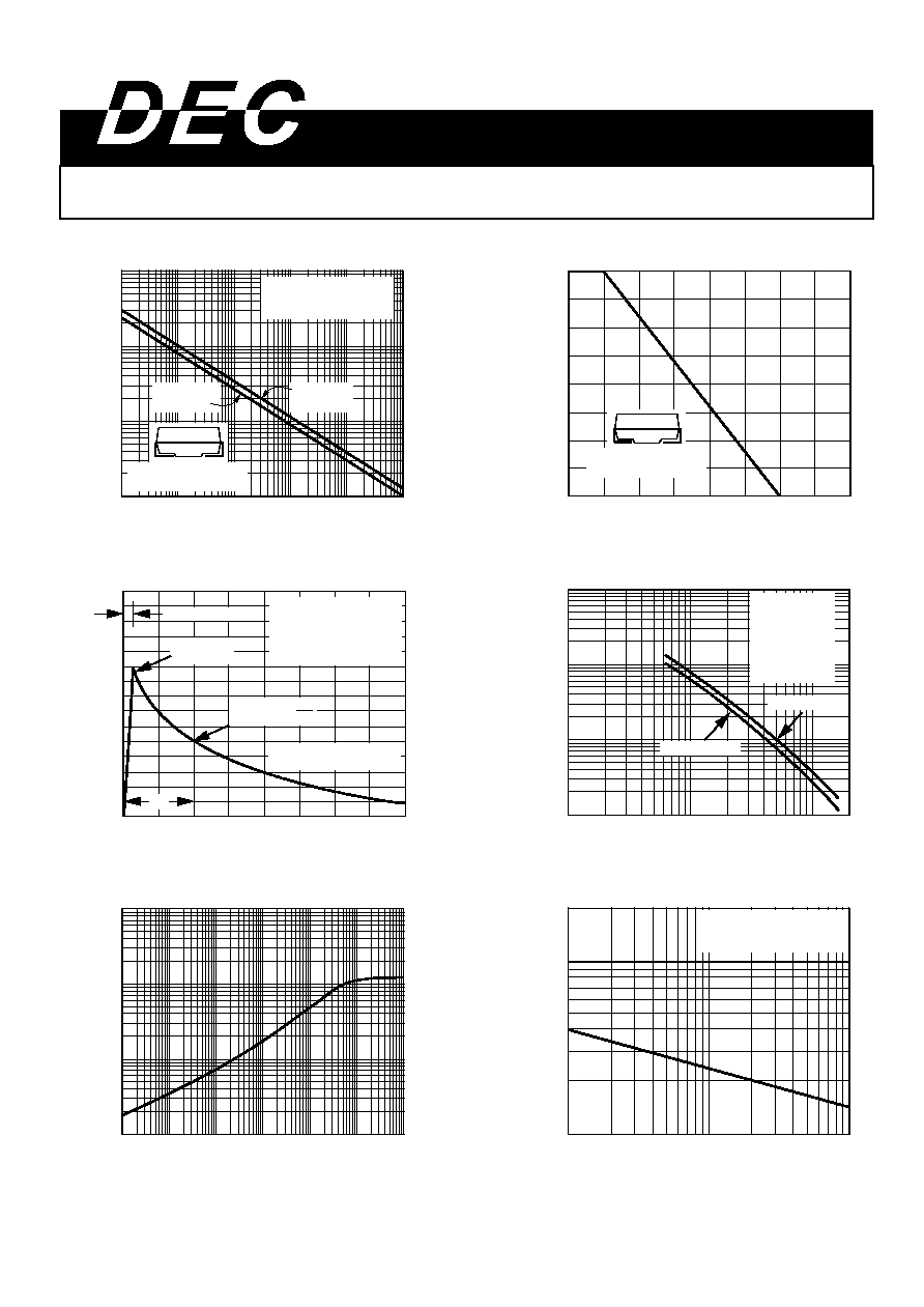
RATINGS AND CHARACTERISTIC CURVES SMAJ5.0 THRU SMAJ188CA
0
25
50
75
100
0
75
25
50
100
125
150
175
200
P
e
a
k
P
u
l
s
e
P
o
w
e
r
(
P
P
P
)
o
r
C
u
r
r
e
n
t
(
I
P
P
M
)
D
e
r
a
t
i
n
g
i
n
P
e
r
c
e
n
t
a
g
e
,
%
T
A
, Ambient Temperature ( C )
1
5
10
50
100
t
p
, P ulse Duration (sec)
Fig. 2 – P uls e Derating C urve
P
P
P
M
,
P
e
a
k
P
u
l
s
e
P
o
w
e
r
(
k
W
)
Fig. 1 –
P eak P uls e P ower R ating C ur ve
0.1
1
10
100
0.1
s
1.0
s
1 0
s
t
d
, P ulse Width (sec.)
100
s
1.0ms
10ms
0.2 x 0.2" (5.0 x 5.0mm)
C opper P ad Areas
0.2 x 0.2" (5.0 x 5.0mm)
C opper P ad Areas
T
r
a
n
s
i
e
n
t
T
h
e
r
m
a
l
I
m
p
e
d
a
n
c
e
(
o
C
/
W
)
F ig. 5 – T ypical Trans ient T hermal
Impedance
Non-repetitive P ulse
Waveform shown in F ig. 3
T
A
= 25
o
C
F ig. 6 - Maximum Non-R epetitive F orwar d
S urge C urrent Uni-Directional Onl y
I
F
S
M
,
P
e
a
k
F
o
r
w
a
r
d
S
u
r
g
e
C
u
r
r
e
n
t
(
A
)
Number of C ycles at 60 Hz
C
J
,
J
u
n
c
t
i
o
n
C
a
p
a
c
i
t
a
n
c
e
(
p
F
)
10
100
1,000
10,000
10
1
100
200
V
WM
, R everse S tand-off Voltage (V )
T
J
= 25
o
C
f = 1.0MHz
V sig = 50mV p-p
Measured at
S tand-Off
Voltage, V
WM
Uni-Directional
B i-Directional
10
50
100
200
T
J
= T
J
max.
8.3ms S ingle Half S ine-Wave
(J E DE C Method)
Fig. 4 – Typical J unction C apacitance
1
10
100
1000
0.001
0.01
0.1
1
10
100
1000
0
50
100
150
I
P
P
M
,
P
e
a
k
P
u
l
s
e
C
u
r
r
e
n
t
,
%
I
R
S
M
Fig. 3 – P uls e Waveform
T
J
= 25
o
C
P ulse Width (td)
is defined as the point
where the peak current
decays to 50% of I
P P M
tr = 10
S
P eak Value
I
P P M
Half Value IP P
I
P P M
2
td
10/1000
S W aveform
as defined by R .E .A.
0
1.0
2.0
3.0
4.0
t , Time (ms)
S MAJ 5.0 --
S MAJ 78
S MAJ 85 --
S MAJ 188