 | –≠–ª–µ–∫—Ç—Ä–æ–Ω–Ω—ã–π –∫–æ–º–ø–æ–Ω–µ–Ω—Ç: DS1045-4 | –°–∫–∞—á–∞—Ç—å:  PDF PDF  ZIP ZIP |

1 of 6
071700
FEATURES
All-silicon time delay
Two programmable outputs from a single
input produce output-to-output delays
between 9 and 84 ns depending on device
type
Programmable via four input pins
Programmable increments of 3 to 5 ns with a
minimum of 9 ns and a maximum of 84 ns
Output pulse is a reproduction of input pulse
after
Delay with both leading and trailing edge
accuracy
Standard 16-pin DIP or surface mount 16-pin
SOIC
Auto-insertable
Low-power CMOS design is TTL-compatible
PIN ASSIGNMENT
PIN DESCRIPTION
IN -
Delay
Line
Input
OUTA, OUTB
- Delay Line Outputs
A0-A3
- Parallel Program Inputs
for OUT1
B0-B3
- Parallel Program Inputs
for OUT2
EA
,
EB
- Enable A and B Inputs
V
CC
- +5V Input
GND -
Ground
DESCRIPTION
The DS1045 is a programmable silicon delay line having one input and two 4-bit programmable delay
outputs. Each 4-bit programmable output offers the user 16 possible delay values to select from, starting
with a minimum inherent DS1045 delay of 9 ns and a maximum achievable delay in the standard DS1045
family of 84 ns. The standard DS1045 product line provides the user with three devices having uniform
delay increments of 3, 4, and 5 ns, depending on the device. Table 1 presents standard device family and
delay capability. Additionally, custom delay increments are available for special order through Dallas
Semiconductor.
The DS1045 is TTL and CMOS-compatible and capable of driving ten 74LS-type loads. The output
produced by the DS1045 is both rising and falling edge precise. The DS1045 programmable silicon
delay line has been designed as a reliable, economic alternative to hybrid programmable delay lines. It is
offered in a standard 16-pin auto-insertable DIP and a space-saving surface mount 16-pin SOIC package.
DS1045
4-Bit Dual Programmable Delay Line
www.dalsemi.com
IN
V
CC
EA
A0
A1
A2
A3
GND
V
CC
EB
OUTB
B0
B1
B2
B3
OUTA
16
15
14
13
12
11
10
9
1
2
3
4
5
6
7
8
IN
V
CC
16
1
V
CC
EA
A0
A1
A2
A3
GND
EB
OUTB
B0
B1
B2
B3
OUTA
2
3
4
5
6
7
8
15
14
13
12
11
10
9
DS1045 16-Pin DIP
See Mech. Drawings
Section
DS1045S 16-Pin SOIC (300-mil)
See Mech. Drawings
Section
DS1045
2 of 6
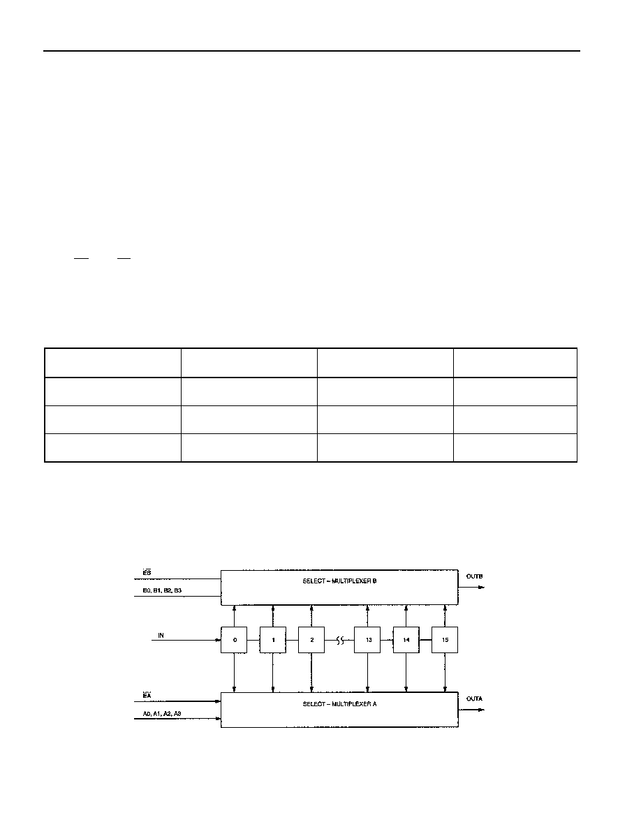
PARALLEL PROGRAMMING
Parallel programming of the DS1045 is accomplished via the set of parallel inputs A0-A3 and B0-B3 as
shown in Figure 1. Parallel input A0-A3 and B0-B3 accept TTL levels and are used to set the delay
values of outputs OUTA and OUTB, respectively. Sixteen possible delay values between the minimum
9 ns delay and the maxi-mum delay of the DS1045-x device version can be selected using the parallel
programming inputs A0-A3 or B0-B3 (see Table 2, "Delay vs. Programmed Input"). For example, the
DS1045-3 outputs OUTA or OUTB and can be programmed to produce 16 possible delays between the
9 ns (minimum) and the 54 ns (maximum) in 3 ns increment levels.
For applications that do not require frequent reprogramming, the parallel inputs can be set using fixed
logic levels, as would be produced by jumpers, DIP switches, or TTL levels as produced by computer
systems. Maximum flexibility in parallel programming can be achieved when inputs are set by computer-
generated data. By using the enable input pins for each respective programmed output and observing the
input setup (t
DSE
) and hold time (t
DHE
) requirements, data can be latched on an 8-bit bus. If the enable
pins,
EA
and
EB
, are not used to latch data, they should be set to a logic level 1. After each change in
the programmed delay value, a settling time (t
EDV
) or (t
PDV
) is required before the delayed output signal is
reliably produced. Since the DS1045 is a CMOS design, undefined input pins should be connected to
well defined logic levels and not left floating.
PART NUMBER TABLE Table 1
PART NUMBER
STEP ZERO DELAY
MAX DELAY TIME
MAX DELAY
TOLERANCE
DS1045-3
9
±
=1 ns
54 ns
±
2.5 ns
DS1045-4
9
±
=1 ns
69 ns
±
3.3 ns
DS1045-5
9
±
=1 ns
84 ns
±
4.1 ns
NOTE:
Additional delay step times are available from Dallas Semiconductor by special order. Consult factory
for availability.
BLOCK DIAGRAM Figure 1

DS1045
3 of 6
DELAY VS. PROGRAMMED VALUE Table 2
PART NUMBER
OUTPUT DELAY VALUE
DS1045-3
9 12 15 18 21 24 27 30 33 36 39 42 45 48 51 54
DS1045-4
9 13 17 21 25 29 33 37 41 45 49 53 57 61 65 69
DS1045-5
9 14 19 24 29 34 39 44 49 54 59 64 69 74 79 84
PROGRAM VALUES FOR EACH DELAY VALUE
A0 OR B0
0
1
0
1
0
1
0
1
0
1
0
1
0
1
0
1
A1 OR B1
0
0
1
1
0
0
1
1
0
0
1
1
0
0
1
1
A2 OR B2
0
0
0
0
1
1
1
1
0
0
0
0
1
1
1
1
A3 OR B3
0
0
0
0
0
0
0
0
1
1
1
1
1
1
1
1
DS1045 TEST CIRCUIT Figure 2
TEST SETUP DESCRIPTION
Figure 2 illustrates the hardware configuration used for measuring the timing parameters of the DS1045.
The input waveform is produced by a precision pulse generator under software control. Time delays are
measured by a time interval counter (20 ps resolution) connected to the output. The DS1045 parallel
inputs are controlled by an interface to a central computer. All measurements are fully automated with
each instrument controlled by the computer over an IEEE 488 bus.

DS1045
4 of 6
ABSOLUTE MAXIMUM RATINGS*
Voltage on Any Pin Relative to Ground
-1.0V to +7.0V
Operating Temperature
0
∞
C to 70
∞
C
Storage Temperature
-55
∞
C to +125
∞
C
Soldering Temperature
See J-STD-020A specification
Short Circuit Output Current
50 mA for 1 second
* This is a stress rating only and functional operation of the device at these or any other conditions above
those indicated in the operation sections of this specification is not implied. Exposure to absolute
maximum rating conditions for extended periods of time may affect reliability.
RECOMMENDED DC OPERATING CONDITIONS
(0
∞
C to 70
∞
C)
PARAMETER
SYMBOL
TEST CONDITION
MIN
TYP
MAX
UNITS NOTES
Supply Voltage
V
CC
4.75
5.0
5.25
V
1
Input Logic 1
V
IH
2.2
V
CC
+0.5
V
1
Input Logic 0
V
IL
-0.5
0.8
µ
A
1
Input Leakage
I
I
0
V
I
V
CC
-1.0
+1.0
µ
A
Active Current
I
CC
V
CC
=5.25V
PERIOD=1
µ
s
35.0
mA
Logic 1 Output
Current
I
OH
V
CC
= 4.75V V
OH
=
4.0V
-1.0
mA
Logic 0 Output
Current
I
OL
V
CC
= 4.75V V
OL
=
0.5V
8
mA
DC ELECTRICAL CHARACTERISTICS
(0∞C to 70∞C; V
CC
5V + 5%)
PARAMETER
SYMBOL
MIN
TYP
MAX
UNITS
NOTES
Period
t
PERIOD
4 x t
WI
ns
Pulse Width
t
WI
100% of output delay size
Input to Output Delay
t
PLH
, t
PHL
Table 1
2
Parallel Input Change to
Delay Invalid
t
PDX
ns
Parallel Input Valid to Delay
Valid
t
PDX
10
ns
Enable Width
t
EW
15
ns
Data Setup to Enable
t
DSE
10
ns
Data Hold from Enable
t
DHE
ns
Enable to Delay Invalid
t
EDX
5
ns
Enable to Delay Valid
t
EDV
15
ns
CAPACITANCE
(T
A
= 25∞C)
PARAMETER
SYMBOL
MIN
TYP
MAX
UNITS
NOTES
Input Capacitance
C
IN
10
pF

DS1045
5 of 6
TEST CONDITIONS
T
A
=25
∞
C
±
=3
∞
C
V
CC
= 5.0V
±
=0.1V
Input Pulse = 3.0V high to 0.0V low
±
=0.1V
Input Source Impedance = 50
maximum
Rise and fall times = 3.0 ns max. between 0.6V and 2.4V
Pulse Width = 250 ns
Period = 500 ns
Output Load = 74F04
Measurement Point = 1.5V on inputs and outputs
Output Load Capacitance = 15 pF
NOTE:
Above conditions are for test only and do not restrict the operation of the device under other data sheet
conditions.
TIMING DIAGRAM: NON-LATCHED PARALLEL MODE, EA , EB = V
IH
TIMING DIAGRAM: LATCHED PARALLEL MODE

DS1045
6 of 6
TIMING DIAGRAM: DS1045 INPUTS TO OUTPUTS
TERMINOLOGY
PERIOD
: The time elapsed between the leading edge of the first pulse and the leading edge of the
following pulse.
t
WI
(Pulse Width): The elapsed time on the pulse between the 1.5V point on the leading edge and the 1.5V
point on the trailing edge, or the 1.5V point on the trailing edge and the 1.5V on the leading edge.
t
RISE
(Input Rise Time): The elapsed time between the 20% and the 80% point on the leading edge of the
input pulse.
t
FALL
(Input Fall Time): The elapsed time between the 80% and the 20% point on the trailing edge of the
input pulse.
t
PLH
(Time Delay, Rising): The elapsed time between the 1.5V point on the leading edge of the input
pulse and the 1.5V point on the leading edge of the output pulse.
t
PHL
(Time Delay, Falling): The elapsed time between the 1.5V point on the trailing edge of the input
pulse and the 1.5V point on the trailing edge of the output pulse.
NOTES:
1.
All voltages are referenced to ground.
2.
@ V
CC
= 5V and 25∞C. Delay accurate on both rising and falling edges within tolerances given in
Table 1.