1 of 20
010202
FEATURES
ß Processor-controlled or stand-alone solid-
state oscillator
ß Frequency changes on the fly
ß Dual, low-jitter, synchronous fixed-
frequency outputs
ß 2-wire serial interface
ß Frequency outputs 4.87kHz to 66.666MHz
±1.25% variation over temperature and
voltage
ß ±0.5% initial tolerance
ß Nonvolatile frequency settings
ß Single 2.7V to 3.6V supply
ß No external components
ß Power-down mode
ß Synchronous output gating
STANDARD FREQUENCY OPTION
Note: x denotes package option
DS1077Lx-40
40.000MHz to 4.87kHz
DS1077Lx-50
50.000MHz to 6.09kHz
DS1077Lx-60
60.000MHz to 7.32kHz
DS1077Lx-66
66.666MHz to 8.13kHz
Contact the factory for the availability of
additional frequencies.
PIN ASSIGNMENTS
OUT1
OUT0
1
2
3
4
GND
SCL
CTRL0
CTRL1
SDA
8
7
6
5
V
CC
PIN DESCRIPTIONS
OUT1
- Main Oscillator Output
OUT0
- Reference Output
V
CC
- Power-Supply Voltage
GND
- Ground
CTRL1
- Control Pin for OUT1
CTRL0
- Control Pin for OUT0
SDA
- 2-Wire Serial Data
Input/Output
SCL
- 2-Wire Serial Clock
ORDERING INFORMATION
Note: XXX denotes frequency option
DS1077LZ-XXX 8-pin 150mil SO
DS1077LU-XXX* 8-pin 118mil µSOP
DESCRIPTION
The DS1077L is a dual-output, programmable, fixed-frequency oscillator requiring no external
components for operation. The DS1077L can be used as a processor-controlled frequency synthesizer or
as a stand-alone oscillator. The two synchronous output operating frequencies are user-adjustable in
submultiples of the master frequency through the use of two on-chip programmable prescalers and
dividers. The specific output frequencies chosen are stored in nonvolatile (EEPROM) memory. The
DS1077L defaults to these values upon power-up.
The DS1077L features a 2-wire serial interface that allows in-circuit on-the-fly programming of the
programmable prescalers (P0 & P1) and divider (N) with the desired values being stored in nonvolatile
(EEPROM) memory. Design changes can be accommodated in-circuit, on-the-fly by simply programming
different values into the device (or reprogramming previously programmed devices). Alternatively, for
fixed-frequency applications previously programmed devices can be used and no connection to the serial
interface is required. Preprogrammed devices can be ordered in customer-requested frequencies.
The DS1077L is available in SO or µSOP packages, allowing the generation of a clock signal easily,
economically, and using minimal board area. Chip-scale packaging is also available on request.
*Future product. Contact factory for availability.
DS1077L
3V EconOscillator/Divider
www.maxim-ic.com
150mil SO
118mil µSOP*

DS1077L
2 of 20
BLOCK DIAGRAM DS1077L Figure 1
PROGRAMMABLE
"N" DIVIDER
CONTROL
LOGIC
(TABLE 1)
CONTROL
LOGIC
2-WIRE
INTERFACE
DIV1
0M1
0M0
1M1
1M0
EN0
SEL0
PDN0
PDN1
CONTROL
REGISTERS
SCL
SDA
INTERNAL
OSCILLATOR
P0 PRESCALER
(M DIVIDER)
P1 PRESCALER
(M DIVIDER)
0M0
0M1
1M0
1M1
MUX
PDN 0
EN0
SEL0
Power-Down
OUT0
CTRL0
Enable
Select
OUT1
DIV1
CTRL1
PDN1
(TABLE 2)
MCLK
Power-Down
Enable

DS1077L
3 of 20
OVERVIEW
A block diagram of the DS1077L is shown in Figure 1. The DS1077L consists of four major components:
1) internal master oscillator, 2) prescalers, 3) programmable divider, and 4) control registers.
The internal oscillator is factory trimmed to provide a master frequency (master clk) that can be routed
directly to the outputs (OUT0 & OUT1) or through separate prescalers (P0 & P1). OUT1 can also be
routed through an additional divider (N).
The prescaler (P0) divides the master clock by 1, 2, 4, or 8 to be routed directly to the OUT0 pin.
The prescaler (P1) divides the master clock by 1, 2, 4, or 8 that can be routed to the OUT1 pin or to the
divider (N) input, which is then routed to the OUT1 pin.
The programmable divider (N) divides the prescaler output (P1) by any number selected between 2 and
1025 to provide the main output (OUT1) or it can be bypassed altogether by use of the DIV1 register bit.
The value of N is stored in the N register.
The control registers are user-programmable through a 2-wire serial interface to determine operating
frequency (values of P0, P1, and N) and modes of operation. The register values are stored in EEPROM
and, therefore, only need to be programmed to alter frequencies and operating modes.
PIN DESCRIPTIONS
OUTPUT 1 (OUT1) ≠ This pin is the main oscillator output; its frequency is determined by the control
register settings for the prescaler P1 (mode bits 1M1 and 1M0) and divider N (DIV WORD).
OUTPUT 0 (OUT0) ≠ A reference output, OUT0, is taken from the output of the reference-select MUX.
Its frequency is determined by the control register settings for CTRL0 and values of prescaler P0 (mode
bits 0M1 and 0M0). (See Table 1.)
CONTROL PIN 0 (CTRL0) ≠ A multifunctional input pin that can be selected as a MUX select, output
enable, and/or a power-down. The user-programmable control register values EN0, SEL0, and PDN0
determine its function. (See Table 1.)
DS1077L
4 of 20
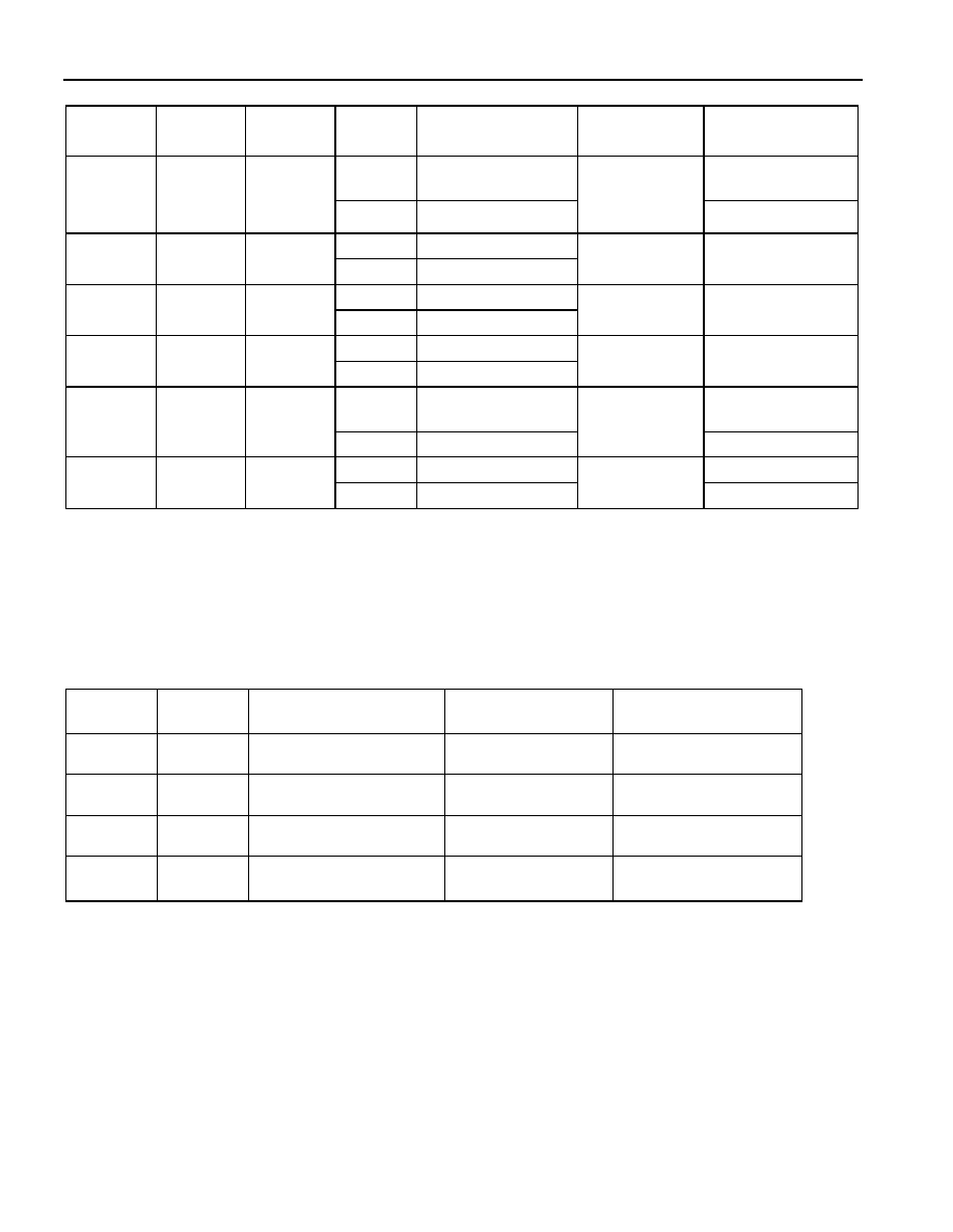
TABLE 1
EN0
(BIT)
SEL0
(BIT)
PDN0
(BIT)
CTRL0
(PIN)
OUT0
(PIN)
CTRL0
FUNCTION
DEVICE
MODE
1
Hi-Z
(OUT1 and OUT2)
Power-Down
0
0
0
0
Hi-Z
Power-Down*
Active
1
Master Clk/M
0
1
0
0
Master Clk
MUX Select
Active
1
Hi-Z
1
0
0
0
Master Clk
Output Enable
Active
1
Hi-Z
1
1
0
0
Master Clk/M
Output Enable
Active**
1
Hi-Z
(OUT1 and OUT2)
Power-Down
X
0
1
0
Master Clk
Power-Down
Active
1
Hi-Z
Power-Down
X
1
1
0
Master Clk/M
Power-Down
Active
*This mode is for applications where OUT0 is not used, but CTRL0 is used as a device shutdown.
**Default Condition
CONTROL PIN 1 (CTRL1) ≠ A multifunctional input pin that can be selected as an output enable
and/or a power-down. Its function is determined by the user-programmable control register value of
PDN1. (See Table 2.)
TABLE 2
PDN1
(BIT)
CTRL1
(PIN)
CTRL1
FUNCTION
OUT 1
DEVICE MODE
0
0
Output Enable
Out Clk
Active*
0
1
Output Enable
Hi-Z
Active*
1
0
Power-Down
Out Clk
Active
1
1
Power-Down
Hi-Z
(OUT1 and OUT2)
Power-Down
*Default Condition
NOTE:
Both CTRL0 and CTRL1 can be configured as power-downs, they are internally "OR" connected so that
either of the control pins may be used to provide a power-down function for the whole device, subject to
appropriate settings of the PDN0 and PDN1 register bits. (See Table 3.)

DS1077L
5 of 20
TABLE 3
PDN0
(BIT)
PDN1
(BIT)
SHUTDOWN CONTROL
0
0
None*
0
1
CTRL1
1
0
CTRL0
1
1
CTRL0 or CTRL1
*CTRL0 performs a power-down if SEL0 and EN0 are both 0. (See Table 1.)
Serial Data Input/Output (SDA) ≠ Input/output pin for the 2-wire serial interface used for data transfer.
Serial Clock Input (SCL) ≠ Input pin for the 2-wire serial interface used to synchronize data movement
on the serial interface.
REGISTER FUNCTIONS
The user-programmable registers can be programmed by the user to determine the mode of operation
(MUX), operating frequency (DIV) and bus settings (BUS). Details of how these registers are
programmed can be found in a later section; in this section the functions of the registers are described.
The register setting are nonvolatile, the values are stored automatically or as required in EEPROM when
the registers are programmed via the SDA and SCL pins.
MUX WORD
MSB
LSB
MSB
LSB
Name
*
PDN1
PDN0
SEL0
EN0
0M1
0M0
1M1
1M0
DIV1
-
-
-
-
-
-
Default setting
0
0
0
1
1
0
0
0
0
0
x
x
x
x
x
x
first data byte
second data byte
*This bit must be set to zero.
DIV1 (bit)
This bit allows the output of the prescaler P1 to be routed directly to the OUT1 pin (DIV1 = 1). The N
divider is bypassed so the programmed value of N is ignored. If DIV1 = 0 (default) the N divider
functions normally.
0M1, 0M0, 1M1, 1M0 (bits)
These bits set the prescalers P0 and P1, to divide by 1, 2, 4, or 8. (See Table 4.)
TABLE 4
0M1
0M0
PRESCALER
P0 DIVISOR
"M"
1M1
1M0
PRESCALER
P1 DIVISOR
"M"
0
0
1*
0
0
1*
0
1
2
0
1
2
1
0
4
1
0
4
1
1
8
1
1
8
*Default Condition