
General Description
The DS12R885 is a functional drop-in replacement for
the DS12885 real-time clock (RTC). The device pro-
vides an RTC/calendar, one time-of-day alarm, three
maskable interrupts with a common interrupt output, a
programmable square wave, and 114 bytes of battery-
backed static RAM. The date at the end of the month is
automatically adjusted for months with fewer than 31
days, including correction for leap years. It also oper-
ates in either 24-hour or 12-hour format with an AM/PM
indicator. A precision temperature-compensated circuit
monitors the status of V
CC
. If a primary power failure is
detected, the device automatically switches to a back-
up supply. The V
BACKUP
pin supports a rechargeable
battery or a super cap and includes an integrated,
always enabled trickle charger. The DS12R885 is
accessed through a multiplexed byte-wide interface,
which supports both Intel and Motorola modes. The
DS12CR887 and DS12R887 integrate the DS12R885
die with a crystal and battery.
Applications
Embedded Systems
Utility Meters
Security Systems
Network Hubs, Bridges, and Routers
Features
Trickle-Charge Capability for a Rechargeable
Battery or Super Cap
Selectable Intel or Motorola Bus Timing
RTC Counts Seconds, Minutes, Hours, Day, Date,
Month, and Year with Leap-Year Compensation to
2100
Interrupt Output with Three Independently
Maskable Interrupt Flags
Time-of-Day Alarm is Once-per-Second to Once-
per-Day
Periodic Rates from 122µs to 500ms
End-of-Clock Update Cycle Flag
14 Bytes of Clock and Control Registers
114 Bytes of General-Purpose RAM with Clear Input
Programmable Square-Wave Output
Automatic Power-Fail Detect and Switch Circuitry
+5.0V or +3.3V Operation
Industrial Temperature Range
DS12CR887 Encapsulated DIP (EDIP) Module with
Integrated Battery and Crystal
DS12R887 BGA Module Surface-Mountable
Package with Integrated Crystal and Rechargeable
Battery
DS12R885/DS12CR887/DS12R887
RTC with Constant-Voltage Trickle Charger
______________________________________________ Maxim Integrated Products
1
Ordering Information
DS12R885
DS83C520
±
R/W
AS
GND
X2
X1
V
CC
V
CC
CRYSTAL
DS
V
BACKUP
SUPER
CAP
AD(0≠7)
SQW
RESET
IRQ
RCLR
CS
MOT
Typical Operating Circuit
Rev 1; 4/04
For pricing, delivery, and ordering information, please contact Maxim/Dallas Direct! at
1-888-629-4642, or visit Maxim's website at www.maxim-ic.com.
PART
TEMP RANGE
PIN-
PA CKA GE
TOP MARK
DS12R885-5
-40∞C to +85∞C
24 SO
(300 mils)
DS12R885-5
DS12R885-33
-40∞C to +85∞C
24 SO
(300 mils)
DS12R885-33
DS12CR887-5
-40∞C to +85∞C
24 EDIP
(700 mils)
DS12CR887-5
D S 12C R887- 33
-40∞C to +85∞C
24 EDIP
(700 mils)
DS12CR887-33
DS12R887-5*
-40∞C to +85∞C 48 BGA
DS12R887-5
DS12R887-33*
-40∞C to +85∞C 48 BGA
DS12R887-33
Pin Configurations appear at end of data sheet.
*Future product--contact factory for availability.

DS12R885/DS12CR887/DS12R887
RTC with Constant-Voltage Trickle Charger
2
_____________________________________________________________________
ABSOLUTE MAXIMUM RATINGS
Stresses beyond those listed under "Absolute Maximum Ratings" may cause permanent damage to the device. These are stress ratings only, and functional
operation of the device at these or any other conditions beyond those indicated in the operational sections of the specifications is not implied. Exposure to
absolute maximum rating conditions for extended periods may affect device reliability.
Voltage Range on V
CC
Pin Relative to Ground .....-0.3V to +6.0V
Operating Temperature Range ...........................-40∞C to +85∞C
Storage Temperature Range .............................-55∞C to +125∞C
Soldering Temperature .......................................See IPC/JEDEC
J-STD-020A Specification
Soldering Temperature (leads, 10s) ................................+260∞C
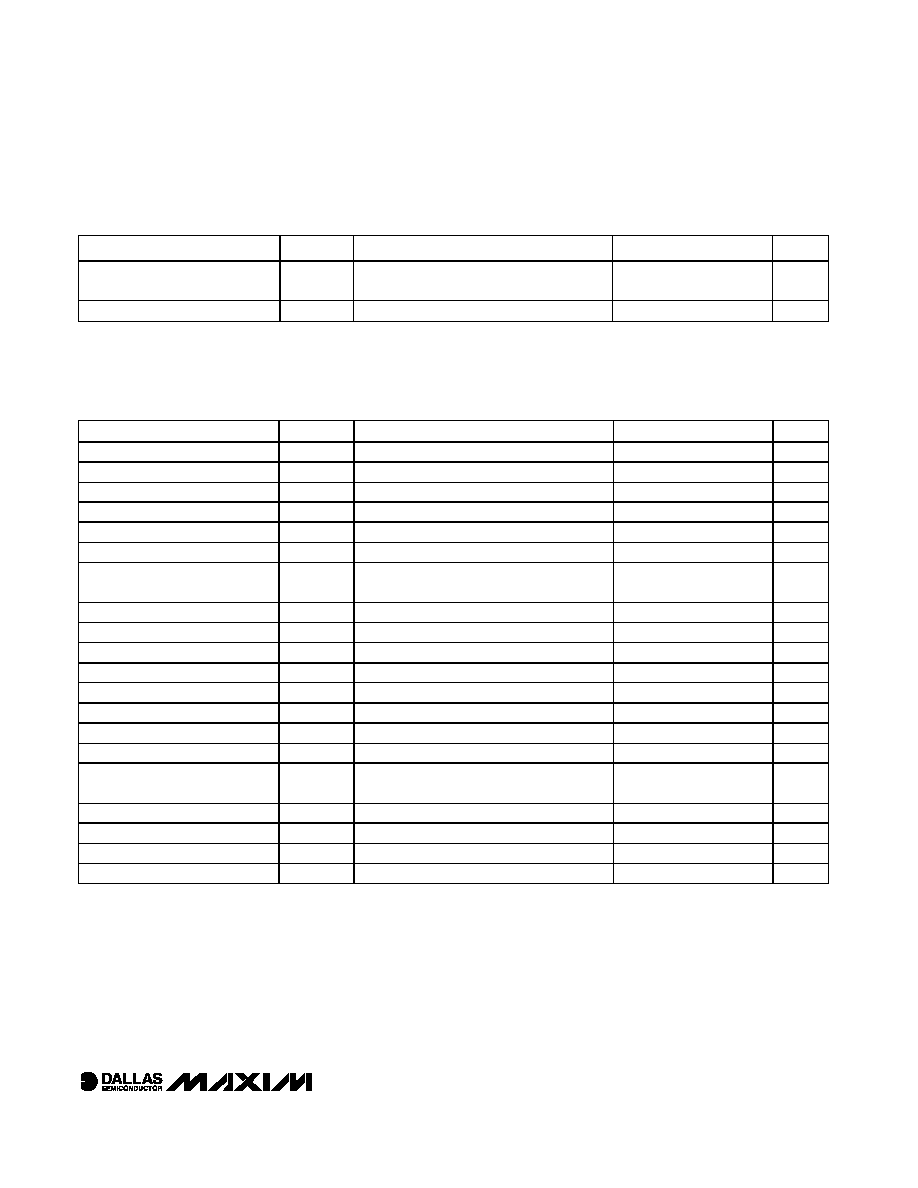
DC ELECTRICAL CHARACTERISTICS
(V
CC
= V
CC(MIN)
to V
CC(MAX)
, T
A
= -40∞C to +85∞C, unless otherwise noted.) (Note 1)
PARAMETER
SYMBOL
CONDITIONS
MIN
TYP
MAX
UNITS
-33
2.97
3.3
3.63
Supply Voltage (Note 2)
V
CC
-5
4.5
5.0
5.5
V
V
BACKUP
Input Voltage
(DS12R885 Only)
V
BACKUP
(Note 2)
2.0
V
OUT
V
Input Logic 1
V
IH
(Note 2)
2.2
V
CC
+
0.3
V
Input Logic 0
V
IL
(Note 2)
-0.3
+0.8
V
-33
0.7
2
V
CC
Power-Supply Current
(Note 3)
I
CC1
-5
0.8
2
mA
-5
0.250
0.5
V
CC
Standby Current (Note 4)
I
CCS
-33
0.140
0.3
mA
Input Leakage
I
IL
-1.0
+1.0
µA
I/O Leakage
I
OL
(Note 5)
-1.0
+1.0
µA
Input Current
I
MOT
(Note 6)
-1.0
+500
µA
Output Current at 2.4V
I
OH
(Note 2)
-1.0
mA
Output Current at 0.4V
I
OL
(Note 2)
4.0
mA
-33
2.7
2.88
2.97
Power-Fail Voltage (Note 2)
V
PF
-5
4.05
4.33
4.5
V
-33
VRT Trip Point
VRT
TRIP
-5
1.3
V
Trickle-Charger Current-Limiting
Resistor
R1
DS12R885 Only
10
k
Trickle-Charger Output Voltage
V
OUT
DS12R885 Only
3.05
V
DS12R885/DS12CR887/DS12R887
RTC with Constant-Voltage Trickle Charger
_____________________________________________________________________
3
DC ELECTRICAL CHARACTERISTICS (DS12R885 Only)
(V
CC
= 0V, V
BACKUP
= 3.2V, T
A
= -40∞C to +85∞C, unless otherwise noted.) (Note 1)
PARAMETER
SYMBOL
CONDITIONS
MIN
TYP
MAX
UNITS
V
BACKUP
Current (OSC On);
T
A
= +25∞C, V
BACKUP
= 3.0V
I
BACKUP2
(Note 7)
800
1000
nA
V
BACKUP
Current (Oscillator Off)
I
BACKUPDR
(Note 7)
100
nA
AC ELECTRICAL CHARACTERISTICS
(V
CC
= 4.5V to 5.5V, T
A
= -40∞C to +85∞C.) (Note 1)
PARAMETER
SYMBOL
CONDITIONS
MIN
TYP
MAX
UNITS
Cycle Time
t
CYC
180
DC
ns
Pulse Width, DS Low or R/
W High
PW
EL
80
ns
Pulse Width, DS High or R/
W Low
PW
EH
65
ns
Input Rise and Fall
t
R
, t
F
30
ns
R/
W Hold Time
t
RWH
0
ns
R/
W Setup Time Before DS/E
t
RWS
10
ns
Chip-Select Setup Time Before
DS or R/
W
t
CS
5
ns
Chip-Select Hold Time
t
CH
0
ns
Read-Data Hold Time
t
DHR
5
35
ns
Write-Data Hold Time
t
DHW
0
ns
Address Valid Time to AS Fall
t
ASL
20
ns
Address Hold Time to AS Fall
t
AHL
5
ns
Delay Time DS/E to AS Rise
t
ASD
10
ns
Pulse Width AS High
PW
ASH
30
ns
Delay Time, AS to DS/E Rise
t
ASED
35
ns
Output Data Delay Time from DS
or R/
W
t
DDR
(Note 8)
15
60
ns
Data Setup Time
t
DSW
50
ns
Reset Pulse Width
t
RWL
5
µs
IRQ Release from DS
t
IRDS
0
2
µs
IRQ Release from RESET
t
IRR
0
2
µs

DS12R885/DS12CR887/DS12R887
RTC with Constant-Voltage Trickle Charger
4
_____________________________________________________________________
AC ELECTRICAL CHARACTERISTICS
(V
CC
= 2.97V to 3.63V, T
A
= -40∞C to +85∞C.) (Note 1)
PARAMETER
SYMBOL
CONDITIONS
MIN
TYP
MAX
UNITS
Cycle Time
t
CYC
280
DC
ns
Pulse Width, DS Low or R/
W High
PW
EL
130
ns
Pulse Width, DS High or R/
W Low
PW
EH
90
ns
Input Rise and Fall
t
R
, t
F
30
ns
R/
W Hold Time
t
RWH
0
ns
R/
W Setup Time Before DS
t
RWS
15
ns
Chip-Select Setup Time Before
DS or R/
W
t
CS
8
ns
Chip-Select Hold Time
t
CH
0
ns
Read-Data Hold Time
t
DHR
5
55
ns
Write-Data Hold Time
t
DHW
0
ns
Address Valid Time to AS Fall
t
ASL
30
ns
Address Hold Time to AS Fall
t
AHL
15
ns
Delay Time DS to AS Rise
t
ASD
15
ns
Pulse Width AS High
PW
ASH
45
ns
Delay Time, AS to DS Rise
t
ASED
55
ns
Output Data Delay Time from DS
or R/
W
t
DDR
(Note 8)
20
80
ns
Data Setup Time
t
DSW
70
ns
Reset Pulse Width
t
RWL
5
µs
IRQ Release from DS
t
IRDS
0
2
µs
IRQ Release from RESET
t
IRR
0
2
µs

DS12R885/DS12CR887/DS12R887
RTC with Constant-Voltage Trickle Charger
_____________________________________________________________________
5
PW
ASH
PW
EL
t
ASED
t
CYC
t
RWS
t
CS
t
RWH
t
CH
PW
EH
t
ASD
AD0≠AD7
READ
CS
R/ W
AS
DS
AD0≠AD7
WRITE
t
DHW
t
DHR
t
DDR
t
AHL
t
ASL
t
DSW
Motorola Bus Read/Write Timing
Intel Bus Write Timing
PW
ASH
PW
ASL
PW
EH
t
CS
t
AHL
t
ASL
t
DSW
t
DHW
t
CH
t
ASD
t
ASD
t
CYC
CS
R/W
AS
DS
AD0≠AD7
WRITE