1 of 42
112299
Note:
Some revisions of this device may incorporate deviations from published specifications known as errata. Multiple
revisions of any device may be simultaneously available through various sales channels. For information about device errata,
click here:
http://www.maxim-ic.com/errata
.
FEATURES
ß 80C32-Compatible
- 8051 pin and instruction set compatible
- Four 8-bit I/O ports
- Three 16-bit timer/counters
- 256 bytes scratchpad RAM
- Addresses 64 kB ROM and 64 kB RAM
ß High-speed architecture
- 4 clocks/machine cycle (8032=12)
- DC to 33 MHz (DS80C320)
- DC to 18 MHz (DS80C323)
- Single-cycle instruction in 121 ns
- Uses less power for equivalent work
- Dual data pointer
- Optional variable length MOVX to access
fast/slow RAM/peripherals
ß High integration controller includes:
- Power-fail reset
- Programmable watchdog timer
- Early-warning power-fail interrupt
ß Two full-duplex hardware serial ports
ß 13 total interrupt sources with six external
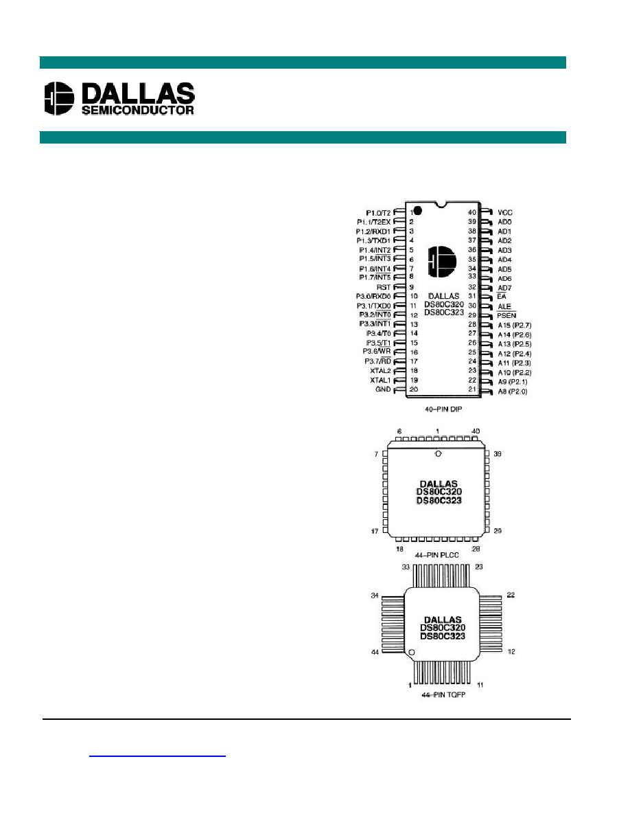
ß Available in 40-pin DIP, 44-pin PLCC and
TQFP
PIN ASSIGNMENT
DS80C320/DS80C323
High-Speed/Low-Power Micro
www.maxim-ic.com
DS80C320/DS80C323
2 of 42
DESCRIPTION
The DS80C320/DS80C323 is a fast 80C31/80C32-compatible microcontroller. Wasted clock and
memory cycles have been removed using a redesigned processor core. As a result, every 8051 instruction
is executed between 1.5 and 3 times faster than the original for the same crystal speed. Typical
applications will see a speed improvement of 2.5 times using the same code and same crystal. The
DS80C320 offers a maximum crystal rate of 33 MHz, resulting in apparent execution speeds of 82.5 MHz
(approximately 2.5X).
The DS80C320/DS80C323 is pin-compatible with all three packages of the standard 80C32 and offers the
same timer/counters, serial port, and I/O ports. In short, the device is extremely familiar to 8051 users but
provides the speed of a 16-bit processor.
The DS80C320 provides several extras in addition to greater speed. These include a second full hardware
serial port, seven additional interrupts, programmable watchdog timer, power-fail interrupt and reset. The
device also provides dual data pointers (DPTRs) to speed block data memory moves. It can also adjust the
speed of off-chip data memory access to between two and nine machine cycles for flexibility in selecting
memory and peripherals.
The DS80C320 operating voltage ranges from 4.25V to 5.5V, making it ideal as a high-performance
upgrade to existing 5V systems. For applications in which power consumption is critical, the DS80C323
offers the same feature set as the DS80C320, but with 2.7V to 5.5V operation.
ORDERING INFORMATION
PART NUMBER
PACKAGE
MAX CLOCK SPEED
TEMPERATURE RANGE
DS80C320-MCG
40-pin plastic DIP
25 MHz
0∞C to +70∞C
DS80C320-QCG
44-pin PLCC
25 MHz
0∞C to +70∞C
DS80C320-ECG
44-pin TQFP
25 MHz
0∞C to +70∞C
DS80C320-MNG
40-pin plastic DIP
25 MHz
-40∞C to +85∞C
DS80C320-QNG
44-pin PLCC
25 MHz
-40∞C to +85∞C
DS80C320-ENG
44-pin TQFP
25 MHz
-40∞C to +85∞C
DS80C320-MCL
40-pin plastic DIP
33 MHz
0∞C to +70∞C
DS80C320-QCL
44-pin PLCC
33 MHz
0∞C to +70∞C
DS80C320-ECL
44-pin TQFP
33 MHz
0∞C to +70∞C
DS80C320-MNL
40-pin plastic DIP
33 MHz
-40∞C to +85∞C
DS80C320-QNL
44-pin PLCC
33 MHz
-40∞C to +85∞C
DS80C320-ENL
44-pin TQFP
33 MHz
-40∞C to +85∞C
DS80C323-MCD
40-pin plastic DIP
18 MHz
0∞C to +70∞C
DS80C323-QCD
44-pin PLCC
18 MHz
0∞C to +70∞C
DS80C323-ECD
44-pin TQFP
18 MHz
0∞C to +70∞C
DS80C320/DS80C323
3 of 42
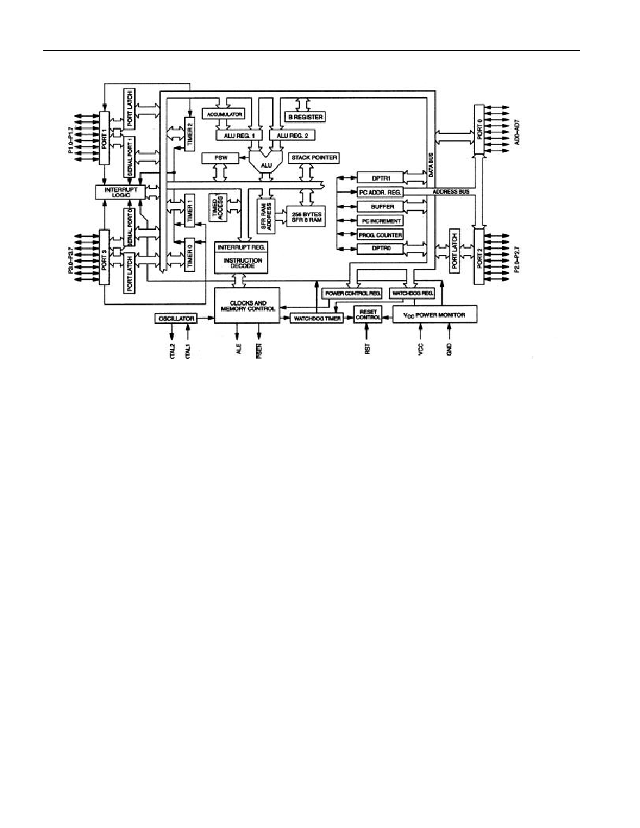
DS80C320 BLOCK DIAGRAM Figure 1
DS80C320/DS80C323
4 of 42
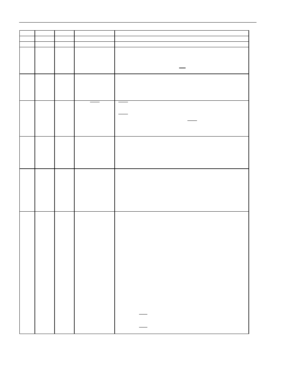
PIN DESCRIPTION Table 1
DIP
PLCC
TQFP
SIGNAL NAME
DESCRIPTION
40
44
38
V
CC
V
CC
- +5V. (+3V DS80C323)
20
22, 23
16, 17
GND
GND - Digital circuit ground.
9
10
4
RST
RST - Input. The RST input pin contains a Schmitt voltage input to
recognize external active high Reset inputs. The pin also employs an
internal pulldown resistor to allow for a combination of wired OR
external Reset sources. An RC is not required for power-up, as the
device provides this function internally.
18
19
20
21
14
15
XTAL2
XTAL1
XTAL1, XTAL2 - The crystal oscillator pins XTAL1 and XTAL2
provide support for parallel resonant, AT cut crystals. XTAL1 acts
also as an input in the event that an external clock source is used in
place of a crystal. XTAL2 serves as the output of the crystal
amplifier.
29
32
26
PSEN
PSEN
- Output. The Program Store Enable output. This signal is
commonly connected to external ROM memory as a chip enable.
PSEN
will provide an active low pulse width of 2.25 XTAL1 cycles
with a period of four XTAL1 cycles.
PSEN
is driven high when data
memory (RAM) is being accessed through the bus and during a reset
condition.
30
33
27
ALE
ALE ≠ Output. The Address Latch Enable output functions as a
clock to latch the external address LSB from the multiplexed
address/data bus. This signal is commonly connected to the latch
enable of an external 373 family transparent latch. ALE has a pulse
width of 1.5 XTAL1 cycles and a period of four XTAL1 cycles. ALE
is forced high when the device is in a Reset condition.
39
38
37
36
35
34
33
32
43
42
41
40
39
38
37
36
37
36
35
34
33
32
31
30
AD0
AD1
AD2
AD3
AD4
AD5
AD6
AD7
AD0-7 (Port 0) - I/O. Port 0 is the multiplexed address/data bus.
During the time when ALE is high, the LSB of a memory address is
presented. When ALE falls, the port transitions to a bi-directional
data bus. This bus is used to read external ROM and read/write
external RAM memory or peripherals. The Port 0 has no true port
latch and can not be written directly by software. The reset condition
of Port 0 is high. No pullup resistors are needed.
1-8
2-9
40-44
1-3
P1.0-P1.7
Port 1 - I/O. Port 1 functions as both an 8-bit bi-directional I/O port
and an alternate functional interface for Timer 2 I/O, new External
Interrupts, and new Serial Port 1. The reset condition of Port 1 is with
all bits at a logic 1. In this state, a weak pullup holds the port high.
This condition also serves as an input mode, since any external
circuit that writes to the port will overcome the weak pullup. When
software writes a 0 to any port pin, the device will activate a strong
pulldown that remains on until either a 1 is written or a reset occurs.
Writing a 1 after the port has been at 0 will cause a strong transition
driver to turn on, followed by a weaker sustaining pullup. Once the
momentary strong driver turns off, the port once again becomes the
output high (and input) state. The alternate modes of Port 1 are
outlined as follows:
Port
Alternate
Function
1
2
40
P1.0
T2
External I/O for Timer/Counter 2
2
3
41
P1.1
T2EX
Timer/Counter 2 Capture/Reload Trigger
3
4
42
P1.2
RXD1
Serial Port 1 Input
4
5
43
P1.3
TXD1
Serial Port 1 Output
5
6
44
P1.4
INT2
External Interrupt 2 (Positive Edge Detect)
6
7
1
P1.5
INT3
External Interrupt 3 (Negative Edge Detect)
7
8
2
P1.6
INT4
External Interrupt 4 (Positive Edge Detect)
8
9
3
P1.7
INT5
External Interrupt 5 (Negative Edge Detect)
DS80C320/DS80C323
5 of 42
DIP
PLCC
TQFP
SIGNAL NAME
DESCRIPTION
21
22
23
24
25
26
27
28
24
25
26
27
28
29
30
31
18
19
20
21
22
23
24
25
A8 (P2.0)
A9 (P2.1)
A10 (P2.2)
A11 (P2.3)
A12 (P2.4)
A13 (P2.5)
A14 (P2.6)
A15 (P2.7)
A15-A8 (Port 2) - Output. Port 2 serves as the MSB for external
addressing. P2.7 is A15 and P2.0 is A8. The device will
automatically place the MSB of an address on P2 for external ROM
and RAM access. Although Port 2 can be accessed like an ordinary
I/O port, the value stored on the Port 2 latch will never be seen on the
pins (due to memory access). Therefore writing to Port 2 in software
is only useful for the instructions MOVX A, @Ri or MOVX @Ri, A.
These instructions use the Port 2 internal latch to supply the external
address MSB. In this case, the Port 2 latch value will be supplied as
the address information.
10-17
11,
13-19
5, 7-13
P3.0-P3.7
Port 3 - I/O. Port 3 functions as both an 8-bit bi-directional I/O port
and an alternate functional interface for External Interrupts, Serial
Port 0, Timer 0 & 1 Inputs,
RD
and
WR
strobes. The reset condition
of Port 3 is with all bits at a logic 1. In this state, a weak pullup holds
the port high. This condition also serves as an input mode, since any
external circuit that writes to the port will overcome the weak pullup.
When software writes a 0 to any port pin, the device will activate a
strong pulldown that remains on until either a 1 is written or a reset
occurs. Writing a 1 after the port has been at 0 will cause a strong
transition driver to turn on, followed by a weaker sustaining pullup.
Once the momentary strong driver turns off, the port once again
becomes both the output high and input state. The alternate modes of
Port 3 are outlined below:
Port
Alternate
Mode
10
11
5
P3.0
RXD0
Serial Port 0 Input
11
13
7
P3.1
TXD0
Serial Port 0 Output
12
14
8
P3.2
INT0
External Interrupt 0
13
15
9
P3.3
INT1
External Interrupt 1
14
16
10
P3.4
T0
Timer 0 External Input
15
17
11
P3.5
T1
Timer 1 External Input
16
18
12
P3.6
WR
External Data Memory Write Strobe
17
19
13
P3.7
RD
External Data Memory Read Strobe
31
35
29
EA
EA
- Input. This pin must be connected to ground for proper
operation.
-
12
34
6
28
NC
NC - Reserved. These pins should not be connected. They are
reserved for use with future devices in this family.
-
1
39
NC - Reserved. These pins are reserved for additional ground pins
on future products.
80C32 COMPATIBILITY
The DS80C320/DS80C323 is a CMOS 80C32-compatible microcontroller designed for high
performance. In most cases it will drop into an existing 80C32 design to significantly improve the
operation. Every effort has been made to keep the device familiar to 8032 users, yet it has many new
features. In general, software written for existing 80C32-based systems will work on the
DS80C320/DS80C323. The exception is critical timing since the High-Speed Microcontroller performs
its instructions much faster than the original. It may be necessary to use memories with faster access
times if the same crystal frequency is used.
Application note 57 "DS80C320 Memory Interface Timing" is a useful tool to help the embedded system
designer select the proper memories for her or his application.
The DS80C320/DS80C323 runs the standard 8051 instruction set and is pin-compatible with an 80C32 in
any of three standard packages. It also provides the same timer/counter resources, full-duplex serial port,
256 bytes of scratchpad RAM and I/O ports as the standard 80C32. Timers will default to a 12 clock per