
3010
VOLTAGE-VARIABLE DELAY LINE
T
R
< 1ns
(SERIES 3010)
FEATURES PACKAGE
∑ Varactor Technology
∑ Fast rise time for high frequency applications
∑ Delay continuously adjustable from 2.4ns to 3.4ns
∑ Very narrow device (SIP package)
∑ Stackable for PC board economy
∑ Epoxy encapsulated
∑ Meets or exceeds MIL-D-23859C
FUNCTIONAL DESCRIPTION
The 3010-series devices are continuously variable, single-input, single-
output, passive delay lines. The signal input (IN) is reproduced at the
output (OUT), shifted by a time (T
D
) which is adjusted via an applied
control voltage (VC). This control voltage is positive for the 3010-P and
negative for the 3010-N. The characteristic impedance of the line is
nominally 50 ohms. The rise time (T
R
) of the lines is no more than 1ns, resulting in a 3dB bandwidth of at
least 300MHz. The delay resolution is limited only by that of the control voltage.
data
delay
devices,
inc.
3
G
G
IN
OUT
VC
3010
3010-P: Positive control voltage
3010-N: Negative control voltage
3 7
1 9
6
PIN DESCRIPTIONS
IN Signal
Input
OUT Signal
Output
VC Control
Voltage
G Ground
SERIES SPECIFICATIONS
∑ Varactor voltage range (3010-P): 1.3V (max T
D
) to 11.3V (min T
D
)
∑ Varactor voltage range (3010-N): -1.3V (max T
D
) to -11.3V (min T
D
)
∑ Range of delay variation: 1.0ns minimum
∑ Minimum delay: 2.4ns
± 0.25ns
∑ Impedance: 45 - 68
∑ Output rise time: 1.0ns
max
∑ Bandwidth:
300MHz min
1.3 11.3
6.3
0.0
0.5
1.0
1.5
40
50
60
70
Delay
Impedance
Varactor Voltage (V)
Delay
Variation
(ns)
Impedance
(
)
Typical Delay/Impedance Variation
∑ Overshoot/preshoot:
± 20% max
∑ Operating temperature: -10∞C to +80∞C
∑ Temperature coefficient: 1000
PPM/
∞C max
.020
DIA
Package Dimensions
.100
MIN
.150
MAX
Series
3010
.200
.200
.100
.800
1.08 MAX
IN
OUT
G
G
VC
.380
MAX
2004 Data Delay Devices
Doc #04001
DATA DELAY DEVICES, INC.
1
8/10/2005
3 Mt. Prospect Ave. Clifton, NJ 07013

3010
TYPICAL APPLICATIONS
IN
G
OUT
G
VC
3010-P
1.3V - 11.3V*
+
Rin
r:
Signal source impedance
Rin:
Input termination resistor
Ro:
Output termination resistor
∑
∑
Set Ro to the median impedance value within
the delay adjustment range (50
- 60)
Set Rin = Rout - r
r
Ro
*Reverse polarity for 3010-N.
Analog Interface
IN
G
OUT
G
VC
3010-P
2.6Ro
+
0V - 10V
Vcc
Vee
Vee=-5.2V
Vcc=0V
1.6Ro
Vcc
Vcc or Vee
Vcc
Vcc
IN
G
OUT
G
VC
3010-P
Ro
+
0V - 10V
Vee
Vcc
Vcc, Vee or ≠2V
-2V
Vee
IN
G
OUT
G
VC
3010-N
2.6Ro
+
2.6V ≠ 12.6V
Vcc
Vee
1.6Ro
Vee=-5.2V
Vcc=0V
Vcc
Vcc or Vee
Vcc
Vcc
IN
G
OUT
G
VC
3010-N
Ro
+
2.6V ≠ 12.6V
Vee
Vcc
Vcc, Vee or ≠2V
-2V
Vee
ECL with ≠2V Termination
ECL without ≠2V Termination
Note: The varicap voltage is referenced to the DC level of the input signal. In the case of ECL applications, a
voltage of 0V to 10V (2.6V to 12.6V for the 3010-N) should be applied at pin 6, because the signal line has ≠1.3V
DC level. This assumes the ECL signal has approximately 50% duty cycle.
Doc #04001
DATA DELAY DEVICES, INC.
2
8/10/2005
Tel: 973-773-2299 Fax: 973-773-9672 http://www.datadelay.com
3010
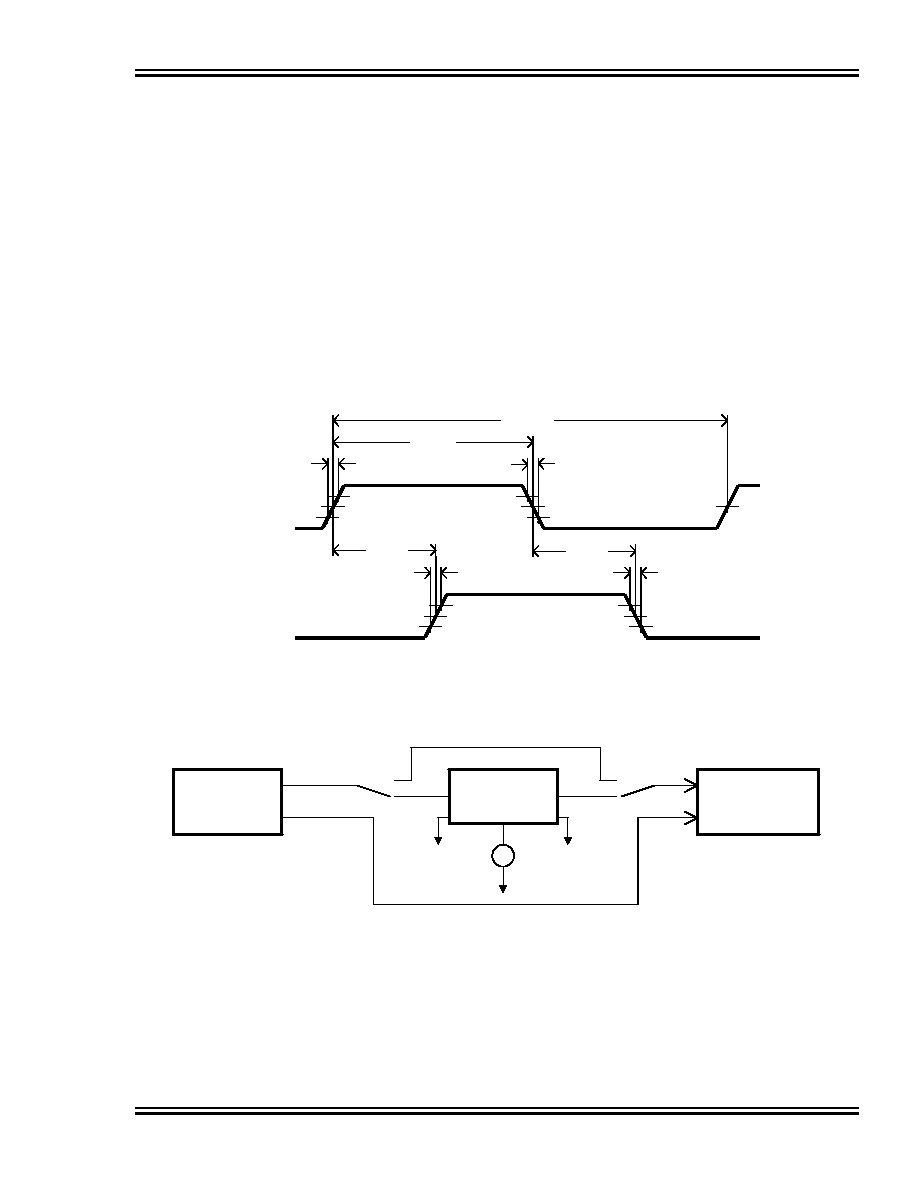
PASSIVE DELAY LINE TEST SPECIFICATIONS
TEST CONDITIONS
INPUT:
OUTPUT:
Ambient Temperature: 25
o
C
± 3
o
C
R
load
: 50
Input Pulse:
High = 1.8V typical
C
load
: <10pf
Low = 0.8V typical
Threshold: 50% (Rising & Falling)
Source Impedance: 50
Max.
Rise/Fall Time:
3.0 ns Max. (measured
at 10% and 90% levels)
Pulse Width:
PW
IN
= 500ns
Period:
PER
IN
= 1000ns
NOTE: The above conditions are for test only and do not in any way restrict the operation of the device.
Timing Diagram For Testing
D
RISE
D
FALL
PER
IN
PW
IN
T
RISE
T
FALL
10%
10%
50%
50%
90%
90%
50%
50%
V
IH
V
IL
V
OH
V
OL
INPUT
SIGNAL
OUTPUT
SIGNAL
T
RISE
T
FALL
10%
10%
90%
90%
IN
OUT
OUT (50
)
TRIG
IN (50
)
TRIG
Test Setup
DEVICE UNDER
TEST (DUT)
OSCILLOSCOPE
PULSE
GENERATOR
+
VC
Doc #04001
DATA DELAY DEVICES, INC.
3
8/10/2005
3 Mt. Prospect Ave. Clifton, NJ 07013