 | –≠–ª–µ–∫—Ç—Ä–æ–Ω–Ω—ã–π –∫–æ–º–ø–æ–Ω–µ–Ω—Ç: 118AMM | –°–∫–∞—á–∞—Ç—å:  PDF PDF  ZIP ZIP |

Figure 1. ADS-118/118A Functional Block Diagram
FEATURES
∑
12-bit resolution
∑
5MHz minimum sampling rate
∑
Functionally complete
∑
Small 24-pin DDIP
∑
Requires only ±5V supplies
∑
Low-power, 1.3 Watts
∑
Outstanding dynamic performance
∑
No missing codes over full military temperature range
∑
Edge-triggered, no pipeline delay
∑
Ideal for both time and frequency-domain applications
GENERAL DESCRIPTION
DATEL's ADS-118 and ADS-118A are 12-bit, 5MHz, sampling
A/D converters packaged in space-saving 24-pin DDIP's. The
ADS-118 offers an input range of ±1V and has three-state
outputs. The ADS-118A has an input range of ±1.25V and
features direct adjustment of offset error.
These functionally complete low-power devices (1.3 Watts)
contain an internal fast-settling sample/hold amplifier, a 12-bit
subranging A/D converter, a precise voltage reference, timing/
control logic, and error-correction circuitry. All timing and
control logic operates from the rising edge of a single start
convert pulse. Digital input and output levels are TTL. Models
are available for use in either commercial (0 to +70∞C) or
military (≠55 to +125∞C) operating temperature ranges.
Applications include radar, transient signal analysis, process
control, medical/graphic imaging, and FFT spectrum analysis.
Æ
Æ
I N N O V A T I O N a n d E X C E L L E N C E
ADS-118, ADS-118A
12-Bit, 5MHz, Low-Power
Sampling A/D Converters
DATEL, Inc., 11 Cabot Boulevard, Mansfield, MA 02048-1151 (U.S.A.)
∑
Tel: (508) 339-3000 Fax: (508) 339-6356
∑
For immediate assistance: (800) 233-2765
INPUT/OUTPUT CONNECTIONS
PIN
FUNCTION
PIN
FUNCTION
1
BIT 12 (LSB)
24
NO CONNECTION
2
BIT 11
23
ANALOG GROUND
3
BIT 10
22
NO CONNECTION
4
BIT 9
21
+5V ANALOG SUPPLY
5
BIT 8
20
≠5V SUPPLY
6
BIT 7
19
ANALOG INPUT
7
BIT 6
18
ANALOG GROUND
8
BIT 5
17
ENABLE/OFFSET ADJ.
9
BIT 4
16
START CONVERT
10
BIT 3
15
EOC
11
BIT 2
14
DIGITAL GROUND
12
BIT 1 (MSB)
13
+5V DIGITAL SUPPLY
*
* ADS-118, Pin 17 is ENABLE
ADS-118A, Pin 17 is OFFSET ADJUST
REF
DAC
R
E
G
I
S
T
E
R
R
E
G
I
S
T
E
R
3
-
S
T
A
T
E
O
U
T
P
U
T
R
E
G
I
S
T
E
R
12 BIT 1 (MSB)
11 BIT 2
10 BIT 3
9 BIT 4
8 BIT 5
7 BIT 6
6 BIT 7
5 BIT 9
4 BIT 9
3 BIT 10
2 BIT 11
1 BIT 12 (LSB)
TIMING AND
CONTROL LOGIC
OFFSET ADJUST 17
ANALOG INPUT 19
START CONVERT 16
EOC 15
≠
+
S/H
BUFFER
D
I
G
I
T
A
L
C
O
R
R
E
C
T
I
O
N
L
O
G
I
C
FLASH
ADC
1
FLASH
ADC
2
AMP
21
+5V ANALOG
SUPPLY
20
≠5V SUPPLY
18, 23
ANALOG
GROUND
13
+5V DIGITAL
SUPPLY
14
DIGITAL
GROUND
22, 24
NO CONNECT
(ADS-118A only)
17 ENABLE
(ADS-118A only)

ADS-118/118A
Æ
Æ
2
PARAMETERS
MIN.
TYP.
MAX.
UNITS
Operating Temp. Range, Case
ADS-118/118AMC
0
--
+70
∞C
ADS-118/118AMM, GM, 883
≠55
--
+125
∞C
Thermal Impedance
jc
--
2
--
∞C/Watt
ca
--
23
--
∞C/Watt
Storage Temperature Range
≠65
--
+150
∞C
Package Type
24-pin, metal-sealed, ceramic DDIP or SMT
Weight
0.42 ounces (12 grams)
ABSOLUTE MAXIMUM RATINGS
PARAMETERS
LIMITS
UNITS
+5V Supply (Pins 13, 21)
0 to +6
Volts
≠5V Supply (Pin 20)
0 to ≠6
Volts
Digital Input (Pin 16, 17)
≠0.3 to +V
DD
+0.3
Volts
Analog Input (Pin 19)
±5
Volts
Lead Temperature (10 seconds)
+300
∞C
PHYSICAL/ENVIRONMENTAL
+25∞C
0 to +70∞C
≠55 to +125∞C
ANALOG INPUT
MIN.
TYP.
MAX.
MIN.
TYP.
MAX.
MIN.
TYP.
MAX.
UNITS
Input Voltage Range, ADS-118
--
±1
--
--
±1
--
--
±1
--
Volts
Input Resistance
475
500
--
475
500
--
475
500
--
Input Capacitance
--
6
15
--
6
15
--
6
15
pF
DIGITAL INPUT
Logic Levels
Logic "1"
+2.0
--
--
+2.0
--
--
+2.0
--
--
Volts
Logic "0"
--
--
+0.8
--
--
+0.8
--
--
+0.8
Volts
Logic Loading "1"
--
--
+20
--
--
+20
--
--
+20
µA
Logic Loading "0"
--
--
≠20
--
--
≠20
--
--
≠20
µA
Start Convert Positive Pulse Width
50
100
--
50
100
--
50
100
--
ns
STATIC PERFORMANCE
Resolution
--
12
--
--
12
--
--
12
--
Bits
Integral Nonlinearity (f
in
= 10kHz)
--
±0.75
--
--
±1.0
--
--
±1.5
--
LSB
Differential Nonlinearity (f
in
= 10kHz)
--
±0.5
+0.75
--
±0.5
±0.95
--
±0.75
+0.95
LSB
Full Scale Absolute Accuracy
--
±0.1
±0.5
--
±0.5
±0.75
--
±0.75
±1.5
%FSR
Bipolar Zero Error (Tech Note 2)
--
±0.1
±0.5
--
±0.5
±0.85
--
±0.85
±2.0
%FSR
Bipolar Offset Error (Tech Note 2)
--
±0.1
±0.5
--
±0.5
±1.5
--
±1.5
±2.5
%FSR
Gain Error (Tech Note 2)
--
±0.1
±0.5
--
±0.5
±1.0
--
±1.0
±2.5
%
No Missing Codes (f
in
= 10kHz)
12
--
--
12
--
--
12
--
--
Bits
DYNAMIC PERFORMANCE
Peak Harmonics (≠0.5dB)
dc to 500kHz
--
≠76
≠71
--
≠74
≠70
--
≠72
≠66
dB
500kHz to 1MHz
--
≠75
≠71
--
≠74
≠70
--
≠70
≠65
dB
1MHz to 2.5MHz
--
≠69
≠69
--
≠73
≠67
--
≠66
≠60
dB
Total Harmonic Distortion (≠0.5dB)
dc to 500kHz
--
≠72
≠68
--
≠71
≠67
--
≠70
≠65
dB
500kHz to 1MHz
--
≠71
≠67
--
≠70
≠66
--
≠67
≠63
dB
1MHz to 2.5MHz
--
≠70
≠66
--
≠69
≠65
--
≠66
≠60
dB
Signal-to-Noise Ratio
(w/o distortion, ≠0.5dB)
dc to 500kHz
67
69
--
66
69
--
64
67
--
dB
500kHz to 1MHz
66
69
--
65
68
--
63
66
--
dB
1MHz to 2.5MHz
66
69
--
65
68
--
63
66
--
dB
Signal-to-Noise Ratio
(& distortion, ≠0.5dB)
dc to 500kHz
65
68
--
64
67
--
62
66
--
dB
500kHz to 1MHz
65
68
--
64
67
--
61
65
--
dB
1MHz to 2.5MHz
64
67
--
63
66
--
60
64
--
dB
Noise
--
195
--
--
195
--
--
195
--
µVrms
Two-tone Intermodulation
Distortion (f
in
= 1MHz,
975kHz, f
s
= 5MHz, ≠0.5dB)
--
≠74
--
--
≠74
--
--
≠74
--
dB
Input Bandwidth (≠3dB)
Small Signal (≠20dB input)
--
20
--
--
20
--
--
20
--
MHz
Large Signal (≠0.5dB input)
--
10
--
--
10
--
--
10
--
MHz
Feedthrough Rejection (f
in
= 2.5MHz)
--
80
--
--
80
--
--
80
--
dB
Slew Rate
--
±400
--
--
±400
--
--
±400
--
V/µs
Aperture Delay Time
--
+10
--
--
+10
--
--
+10
--
ns
Aperture Uncertainty
--
3
--
--
3
--
--
3
--
ps rms
FUNCTIONAL SPECIFICATIONS
(T
A
= +25∞C, ±V
DD
= ±5V, 5MHz sampling rate, and a minimum 3 minute warmup unless otherwise specified.)

ADS-118/118A
Æ
Æ
3
the adjustment circuitry shown in Figures 2a and 2b. When
using this circuitry, or any similar offset and gain-calibration
hardware, make adjustments following warmup. To avoid
interaction, always adjust offset before gain.
3. To enable the three-state outputs, connect ENABLE
(pin 17) to a logic "0" (low). To disable, connect pin 17 to
logic "1" (high). The three-state outputs are permanently
enabled in the ADS-118A.
4. Applying a start convert pulse while a conversion is in
progress (EOC = logic "1") will initiate a new and inaccurate
conversion cycle.
+25∞C
0 to +70∞C
≠55 to +125∞C
DYNAMIC PERFORMANCE (Cont.)
MIN.
TYP.
MAX.
MIN.
TYP.
MAX.
MIN.
TYP.
MAX.
UNITS
S/H Acquisition Time
( to ±0.001%FSR, 10V step)
--
85
90
--
85
90
--
85
90
ns
Overvoltage Recovery Time
--
200
--
--
200
--
--
200
--
ns
A/D Conversion Rate
5
--
--
5
--
--
5
--
--
MHz
DIGITAL OUTPUTS
Logic Levels
Logic "1"
+2.4
--
--
+2.4
--
--
+2.4
--
--
Volts
Logic "0"
--
--
+0.4
--
--
+0.4
--
--
+0.4
Volts
Logic Loading "1"
--
--
≠4
--
--
≠4
--
--
≠4
mA
Logic Loading "0"
--
--
+4
--
--
+4
--
--
+4
mA
Delay, Falling Edge of EOC to
Output Data Valid
--
--
20
--
--
20
--
--
20
MHz
Delay, Falling Edge of ENABLE to
Output Data Valid
--
--
10
--
--
10
--
--
10
MHz
Output Coding
Offset Binary
POWER REQUIREMENTS
Power Supply Ranges
+5V Supply
+4.75
+5.0
+5.25
+4.75
+5.0
+5.25
+4.9
+5.0
+5.25
Volts
≠5V Supply
≠4.75
≠5.0
≠5.25
≠4.75
≠5.0
≠5.25
≠4.9
≠5.0
≠5.25
Volts
Power Supply Currents
+5V Supply
--
+205
+220
--
+205
+220
--
+205
+220
mA
≠5V Supply
--
≠80
≠90
--
≠80
≠90
--
≠80
≠90
mA
Power Dissipation
--
1.3
1.5
--
1.3
1.5
--
1.3
1.5
Watts
Power Supply Rejection
--
--
±0.1
--
--
±0.1
--
--
±0.1
%FSR/%V
Footnotes:
This is the time required before the A/D output data is valid once the analog input
is back within the specified range.
The minimum supply voltages of +4.9V and ≠4.9V for ±V
DD
are required for
≠55∞C operation only. The minimum limits are +4.75V and ≠4.75V when
operating at +125∞C
6.02
(SNR + Distortion) ≠ 1.76 + 20 log
Full Scale Amplitude
Actual Input Amplitude
All power supplies should be on before applying a start convert pulse. All
supplies and the clock (start convert pulses) must be present during warmup
periods. The device must be continuously converting during this time.
Input voltage ranges for ADS-118A is ±1.25V
A 100ns wide start convert pulse is used for all production testing. For
applications requiring less than an 5MHz sampling rate, wider start convert
pulses can be used.
NOTE: The device only requires the rising edge of a start convert pulse to
operate.
Effective bits is equal to:
TECHNICAL NOTES
1. Obtaining fully specified performance from the ADS-118
requires careful attention to pc-card layout and power supply
decoupling. The device's analog and digital ground systems
are connected to each other internally. For optimal perfor-
mance, tie all ground pins (14, 18, and 23) directly to a large
analog ground plane beneath the package.
Bypass all power supplies to ground with 4.7µF tantalum
capacitors in parallel with 0.1µF ceramic capacitors. Locate
the bypass capacitors as close to the unit as possible.
2. The ADS-118 achieves its specified accuracies without the
need for external calibration. If required, the device's small
initial offset and gain errors can be reduced to zero using
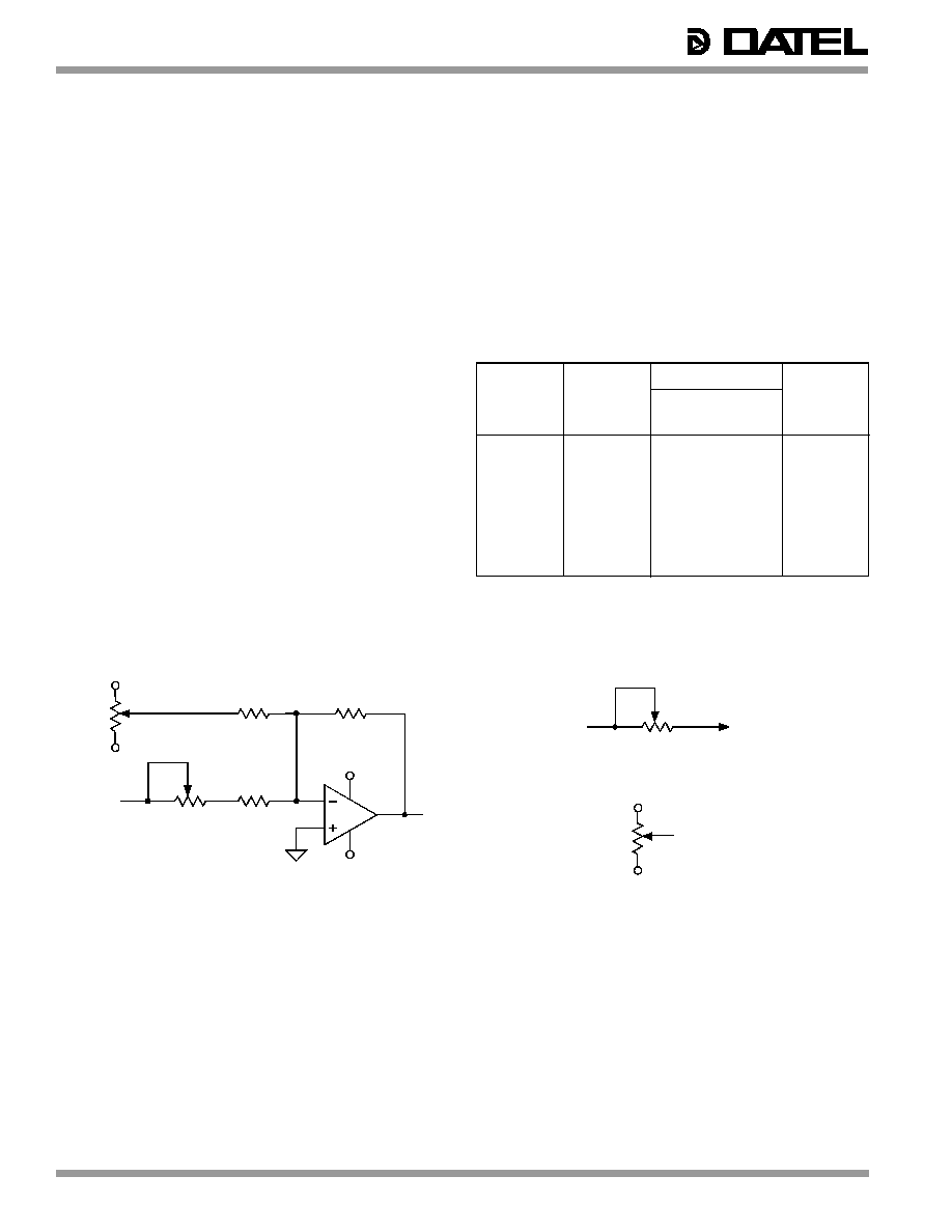
ADS-118/118A
Æ
Æ
4
SIGNAL
INPUT
GAIN
ADJUST
50
To Pin19
of ADS-118A
Potentiometer is at 25
during the device's factory trim procedure.
20k
≠15V (or ≠5V)
+15V (or +5V)
To Pin17
of ADS-118A
ZERO/
OFFSET
ADJUST
To Pin19
of ADS-118
≠15V
SIGNAL
INPUT
GAIN
ADJUST
1.98k
50
+15V
2k
1.2M
20k
≠15V
+15V
ZERO/
OFFSET
ADJUST
CALIBRATION PROCEDURE
Any offset and/or gain calibration procedures should not be
implemented until devices are fully warmed up. To avoid
interaction, offset must be adjusted before gain. The ranges of
adjustment for the circuits in Figures 2a and 2b are guaranteed
to compensate for the ADS-118's initial accuracy errors and
may not be able to compensate for additional system errors.
A/D converters are calibrated by positioning their digital
outputs exactly on the transition point between two adjacent
digital output codes. This can be accomplished by connecting
LED's to the digital outputs and adjusting until certain LED's
"flicker" equally between on and off. Other approaches employ
digital comparators or microcontrollers to detect when the
outputs change from one code to the next.
For the ADS-118, offset adjusting is normally accomplished at
the point where the MSB is a 1 and all other output bits are 0's
and the LSB just changes from a 0 to a 1. This digital output
transition ideally occurs when the applied analog input is
+ΩLSB (+244µV for ADS-118; +305µV for ADS-118A).
Gain adjusting is accomplished when all bits are 1's and the
LSB just changes from a 1 to a 0. This transition ideally occurs
when the analog input is at +full scale minus 1Ω LSB's
(+0.99927V for ADS-118; +1.249085V for ADS-118A).
Zero/Offset Adjust Procedure
1. Apply a train of pulses to the START CONVERT input
(pin 16) so the converter is continuously converting.
2. Apply +244µV (ADS-118) or +305µV (ADS-118A) to the
ANALOG INPUT (pin 19).
Table 1. Output Coding for Bipolar Operation
+FS ≠1 LSB
+0.99951V
1111 1111 1111
+1.2494V
+3/4 FS
+0.75000V
1110 0000 0000
+0.9375V
+1/2 FS
+0.50000V
1100 0000 0000
+0.6250V
0
0.00000V
1000 0000 0000
0.0000V
≠1/2 FS
≠0.50000V
0100 0000 0000
≠0.6250V
≠3/4 FS
≠0.75000V
0010 0000 0000
≠0.9375V
≠FS +1 LSB
≠0.99951V
0000 0000 0001
≠1.2494V
≠FS
≠1.00000V
0000 0000 0000
≠1.2500V
ADS-118
OUTPUT CODING
ADS-118A
INPUT
INPUT
BIPOLAR
RANGE
OFFSET BINARY
RANGE
SCALE
(±1V )
MSB
LSB
(±1.25V )
3. Adjust the offset potentiometer until the output bits are
1000 0000 00000 and the LSB flickers between 0 and 1.
Gain Adjust Procedure
1. Apply +0.99927V (ADS-118) or +1.249085V (ADS-118A) to
the ANALOG INPUT (pin 19).
2. Adjust the gain potentiometer until all output bits are 1's
and the LSB flickers between 1 and 0.
3. To confirm proper operation of the device, vary the input
signal to obtain the output coding listed in Table 1.
Figure 2a. Optional ADS-118 External
Gain and Offset Adjust Circuits
Figure 2b. Optional ADS-118A
Gain and Offset Adjust Circuits

ADS-118/118A
Æ
Æ
5
Note: Scale is approximately 10ns per division.
OUTPUT
DATA
DATA N-1 VALID
DATA N VALID
20ns typ.
INVALID DATA
130ns min.
150ns typ.
START
CONVERT
INTERNAL S/H
N
N+1
100ns typ.
35ns min., 40ns typ., 50ns max.
Acquisition Time
85ns typ.
90ns max.
10ns typ.
EOC
30ns, ±5ns
Conversion Time
140ns typ., 150ns max.
Hold
INVALID DATA
50ns typ.
70ns max.
ADS-118
ADS-118A
19
16
12
11
10
9
8
7
6
5
4
3
2
1
15
17
BIT 1 (MSB)
BIT 2
BIT 3
BIT 4
BIT 5
BIT 6
BIT 7
BIT 8
BIT 9
BIT 10
BIT 11
BIT 12 (LSB)
EOC
ENABLE (1-12)
or OFFSET ADJUST
ANALOG
INPUT
START
CONVERT
A single +5V supply should be used for both the +5V analog and +5V digital.
If separate supplies are used, the difference between the two cannot exceed 100mV.
0.1µF
0.1µF
4.7µF
4.7µF
13, 21
20
18, 23
≠5V
+5V
14
+
+
Figure 3. Typical Connection Diagram
Figure 4. ADS-118/118A Timing Diagram