 | –≠–ª–µ–∫—Ç—Ä–æ–Ω–Ω—ã–π –∫–æ–º–ø–æ–Ω–µ–Ω—Ç: ADS-235S | –°–∫–∞—á–∞—Ç—å:  PDF PDF  ZIP ZIP |

FEATURES
∑
5MHz (ADS-235/236) and 9MHz (ADS-237) sampling rates
∑
Low power
∑
Outstanding dynamic performance
∑
Fully differential or single-ended analog input
∑
100MHz full power input bandwidth
∑
Integral sample-and-hold
∑
Single +5V supply operation
∑
Internally generated DC bias Voltage
∑
3.0/5.0V CMOS compatible digital output
∑
TTL/CMOS compatible digital inputs/outputs
ADS-235, ADS-236, ADS-237
12-Bit, 5MHz and 9MHz
Sampling A/D Converters
GENERAL DESCRIPTION
The ADS-235, ADS-236 and ADS-237 are monolithic, 12-bit,
sampling analog-to-digital converters fabricated in a CMOS
process. The converters are designed for applications where
high speed, wide bandwidth and low power dissipation are
essential. These characteristics are provided through the use
of a fully differential sampling pipeline A/D architecture with
digital error correction logic.
The ADS-235, ADS-236 and ADS-237 offer excellent dynamic
performance while consuming only 300mW. The digital output
circuit is separate and can be powered from either a 3V or 5V
supply allowing the user to interface with 3V logic, if desired.
The ADS-235, ADS-236 and ADS-237 provide the user with
an internally generated DC bias voltage output. This DC bias
voltage is ideal for AC coupled analog input applications.
The units are available in a 28-lead plastic SOIC package
and operate over the 0∞C to 70∞C and ≠40 to +85∞C
temperature ranges.
INPUT/OUTPUT CONNECTIONS
Figure 1. ADS-235, ADS-236 and ADS-237 Functional Block Diagram
PIN FUNCTION
PIN FUNCTION
DATEL, Inc., Mansfield, MA 02048 (USA)
∑
Tel: (508)339-3000, (800)233-2765 Fax: (508)339-6356
∑
Email: sales@datel.com
∑
Internet:
www.datel.com
Æ
Æ
1
CLK, CLOCK
28
BIT 12
2
+DV
S
1, +5V DIG. SUP.
27
BIT 11
3
DGND1
26
BIT 10
4
+DV
S
1, +5V DIG. SUP.
25
BIT 9
5
DGND1
24
BIT 8
6
+AV
S
, +5V ANALOG SUP. 23
BIT 7
7
AGND
22
+DV
S
2, DIG. OUTPUT SUP.
8
V
IN
+, ANALOG INPUT
21
DGND2
9
V
IN
≠, ANALOG INPUT
20
BIT 6
10
V
DC
, DC BIAS OUTPUT
19
BIT 5
11
V
ROUT
, REF. OUT
18
BIT 4
12
V
RIN
, REF. IN
17
BIT 3
13
AGND
16
BIT 2
14
+AV
S
, +5V ANALOG SUP. 15
BIT 1 (MSB)
Reference
4-Bit
Flash A/D
4-Bit
DAC
4-Bit
DAC
Stage 4
2.3 Volt
DC Bias Output
15 Bit 1 (MSB)
16 Bit 2
17 Bit 3
18 Bit 4
19 Bit 5
20 Bit 6
23 Bit 7
24 Bit 8
25 Bit 9
26 Bit 10
27 Bit 11
28 Bit 12 (LSB)
X8
+
≠
+
≠
Digital Delay
and
Error
Correction
Clock
V
ROUT
V
RIN
V
IN
+
V
IN
≠
V
DC
1 CLK
2, 4
+DV
S
1
3, 5
DGND 1
6, 14
+AV
S
7, 13
AGND
22
+DV
S
2
21
DGND 2
9
Stage 3
4-Bit
Flash A/D
Stage 1
X8
S/H
4-Bit
Flash A/D
Â
Â
11
12
8
10

ADS-235, ADS-236, ADS-237
2
Æ
Æ
Second Harmonic, F
IN
=1MHz
ADS-235
--
≠73
--
dB
ADS-236
--
≠86
--
dB
ADS-237
--
≠80
--
dB
Third Harmonic, F
IN
=1MHz
ADS-235
--
≠73
--
dB
ADS-236
--
≠83
--
dB
ADS-237
--
≠77
--
dB
Effective Number Of Bits,
ENOB, F
IN
=1MHz
ADS-235
--
10.3
--
Bits
ADS-236
--
11
--
Bits
ADS-237
--
10.8
--
Bits
Signal to Noise Ratio and
Distortion, SINAD, F
IN
=1MHz
ADS-235
--
64
--
dB
ADS-236
--
68
--
dB
ADS-237
--
66.5
--
dB
Signal to Noise Ratio,
SNR, F
IN
=1MHz
ADS-235
--
65
--
dB
ADS-236
--
68
--
dB
ADS-237
--
67.3
--
dB
Intermodulation Distortion,
IMD, F1=1MHz F2=1.02MHz
ADS-235
--
≠66
--
dB
ADS-236
--
≠68
--
dB
ADS-237
--
≠65
--
dB
Transient Response
--
1
--
Cycle
Over-Voltage Recovery,
0.2V Overdrive
--
2
--
Cycle
TIMING CHARACTERISTICS
Data Output Hold, t
H
--
8
--
ns
Data Output Delay, t
OD
--
8
--
ns
Clock Pulse Width, TPWO, TPW1
ADS-235, ADS-236
90
100
110
ns
ADS-237
106
111
116
ns
Data Latency, t
LAT
--
--
3
Cycles
DC BIAS VOLTAGE OUTPUT
DC Bias Voltage Output,V
DC
--
2.3
--
volts
DC Bias Voltage Current
--
--
1.0
mA
DIGITAL OUTPUTS
Logic Levels
Logic "1", +DV
S
2=5V, V
OH
=2.4V
≠0.2
--
--
mA
Logic "0", +DV
S
2=5V, V
OL
=0.4V
1.6
--
--
mA
Logic "1", +DV
S
2=3V, V
OH
=2.4V
--
≠0.2
--
mA
Logic "0", +DV
S
2=3V, V
OL
=0.4V
--
1.6
--
mA
Output Capacitance
--
5
--
pF
Max. Peak-to-Peak Diff. Voltage
Input Range (V
IN
+ - V
IN
≠)
--
±2.0
--
Volts
Max. Peak-to-Peak Single-Ended
Voltage Input Range
--
4.0
--
Volts
Analog Input Common Mode
Voltage Range (V
IN
+ + V
IN
≠)/2
1.0
2.3
4.0
Volts
Input Bias Current, IB+ or IB≠
≠10
--
10
µA
Differential Input
Current, (IB+ - IB≠)
--
±0.5
--
µA
Input Impedance
1.0
--
--
M
W
Input Capacitance
--
10
--
pF
INTERNAL VOLTAGE REFERENCE
Reference Output Voltage, V
ROUT
--
3.5
--
Volts
Reference Output Current
--
--
1
mA
Reference Temperature Coefficient
ADS-235
--
--
--
ppm/∞C
ADS-236
--
200
--
ppm/∞C
ADS-237
--
50
--
ppm/∞C
REFERENCE VOLTAGE INPUT
Reference Voltage Input, V
RIN
--
3.5
--
Volts
Total Reference Resistance, R
L
--
7.8
--
k
W
Reference Current
--
450
--
µA
PERFORMANCE
Resolution
12
--
--
Bits
Maximum Sample Rate, F
CLK
ADS-235
--
5
--
MHz
ADS-236
5
--
--
MHz
ADS-237
9
--
--
M H z
Minimum Sample Rate
--
0.5
--
M H z
Integral Nonlinearity, F
IN
=DC
ADS-235
--
±2.0
--
LSB
ADS-236, ADS-237
--
±1.0
±2.0
LSB
Differential Nonlinearity,
F
IN
=DC
--
±0.5
±1.0
LSB
Input Offset Error, F
IN
=DC
ADS-235
--
12
--
LSB
ADS-236, ADS-237
--
19
--
LSB
Full Scale Error, F
IN
=DC
ADS-235
--
24
--
LSB
ADS-236, ADS-237
--
32
--
LSB
Aperture Delay, t
AP
--
5
--
ns
Aperture Uncertainty, t
AJ
--
5
--
ps(RMS)
Full Power Input Bandwidth
--
100
--
MHz
Spurious Free Dynamic Range,
SFDR, F
IN
=1MHz
ADS-235
--
73
--
dB
ADS-236
--
83
--
dB
ADS-237
--
77
--
dB
Total Harmonic Distortion,
THD, F
IN
=1MHz
ADS-235
--
≠70
--
dB
ADS-236
--
≠80
--
dB
ADS-237
--
≠75
--
dB
ANALOG INPUTS
MIN.
TYP.
MAX.
UNITS
PARAMETERS
LIMITS
UNITS
PARAMETERS
MIN.
TYP.
MAX.
UNITS
ABSOLUTE MAXIMUM RATINGS
PHYSICAL/ENVIRONMENTAL
FUNCTIONAL SPECIFICATIONS
+AV
S
, +DV
S
1 and +DV
S
2 Supplies
+6.0
Volts
DGND to AGND
0.3
Volts
Analog I/O Pins
AGND to +AV
S
Supply
Volts
Digital I/O Pins
DGND to +DV
S
Supply
Volts
Lead Temperature
(10 seconds, Pin Tips Only)
300
∞C
Operating Temperature Range
ADS-235S
0
--
70
∞C
ADS-236S/ADS-237S
≠40
--
85
∞C
Storage Temperature Range
≠65
--
150
∞C
Thermal Resistance,
q
ja
--
75
∞C/W
Junction Temperature
--
--
150
∞C
Package Type
(T
A
= +25∞C, (ADS-235), TMIN to TMAX (ADS-236/237), +DV
S
1 = +DV
S
2 = +AV
S
= +5V, V
RIN
= 3.5V, F
S
= 5MHz (ADS-235/236) and 9MHz (ADS-237) at a 50% duty
cycle, CL =10pF, and differential analog input unless otherwise specified.)
28-Pin Plastic SOIC
Measured mounted on PC board in free air.
PERFORMANCE (cont.)
MIN.
TYP.
MAX.
UNITS

ADS-235, ADS-236, ADS-237
3
Æ
Æ
Footnotes:
Differential Mode
CLK off and Low
Not specified
No missing codes
For F
S
step to settle to 12-bits accuracy
Power Supply Ranges
+5V Analog Supply, +AV
S
+4.75
5
+5.25
Volts
+5V Digital Supply, +DV
S
1
+4.75
5
+5.25
Volts
+3V Digital Supply, +DV
S
2
+2.7
3
+3.3
Volts
+5V Digital Supply, +DV
S
2
+4.75
5
+5.25
Volts
Power Supply Currents
ADS-235, ADS-236
+AI
S
--
46
--
mA
+DI
S
1
--
13
--
mA
+DI
S
2
--
1
--
mA
ADS-237
+AI
S
--
46
--
mA
+DI
S
1
--
17
--
mA
+DI
S
2
--
2
--
mA
Power Dissipation
ADS-235
--
300
--
mW
ADS-236
--
300
350
mW
ADS-237
--
325
365
mW
Offset Error Sensitivity, 5V±5%
ADS-235
--
±16
--
LSB
ADS-236, ADS-237
--
2
--
LSB
Gain Error Sensitivity, 5V±5%
ADS-235
--
±16
--
LSB
ADS-236, ADS-237
--
30
--
LSB
POWER REQUIREMENTS
MIN.
TYP.
MAX.
UNITS
FUNCTIONAL DESCRIPTION
The ADS-235, ADS-236 and ADS-237 are 12-bit fully
differential pipeline sampling A/D converters with digital error
correction. Referring to the Functional Block Diagram shown in
figure 1, figure 3.1 shows the circuit for the front end differential
in and out sample-and-hold (S/H). The switches are controlled
by an internal sampling clock which is a non-overlapping two
phase signal, ÿ1 and ÿ2, derived from the master sampling
clock. During the sampling phase, ÿ1, the input signal is
applied to the sampling capacitors, C
S
. At the same time the
hold capacitors, C
H
, are discharged to analog ground. At the
falling edge of ÿ1 the input signal is sampled on the bottom
plates of the sampling capacitors. In the next clock phase, ÿ2,
the two bottom plates of the sampling capacitors are connected
together and the holding capacitors are switched to the op-amp
output nodes. The charge then redistributes between C
S
and
C
H
completing one sample and hold cycle.
The sample and hold output is a fully differential representation
of the sampled analog input. The circuit not only performs the
sample-hold function but will also convert a single-ended input
to a fully differential output. During the sampling phase, the V
IN
pins see only the on resistance of a switch and C
S
. The small
values of these components result in a typical full power input
bandwidth of 100MHz for the converters.
As illustrated in the Functional Block Diagram, figure 1, and the
Internal Timing Diagram, figure 2A, three identical pipeline
sub-converter stages, each containing a four-bit flash converter
and a four-bit multiplying digital-to-analog converter, follow the
S/H with the fourth stage being a four-bit flash converter. Each
converter stage in the pipeline will be sampling in one clock
phase and amplifying in the other clock phase. Each sub-
converter clock signal is offset by 180 degrees from the
previous stage clock signal resulting in alternate stages in the
pipeline performing the same operation.
The four-bit output of each of the sub-converter stages is used
by the error correction logic. The output of each stage is input
to a digital delay line which is controlled by the internal
sampling clock. The function of the delay line is to align the
digital outputs in time of the three identical stages with the
output of the fourth stage flash converter before applying the
sixteen bit result to the error correction logic. The error
correction logic uses the supplementary bits to correct any
error that may exist before generating the final twelve-bit digital
data output.
Due to the pipeline nature of this converter, the digital data
representing an analog input sample is output to the digital
Notes: 1. SN: N-th sampling period.
2. HN: N-th holding period.
3. BM, N: M-th stage digital output corresponding to N-th sampled input.
4. DN: Final data output corresponding to N-th sampled input.
Figure 2A. Internal Timing Diagram
Analog Input,
VIN
A/D CLK
1ST Stage
2ND Stage
4TH Stage
Data
Output
SN≠1 HN≠1
SN
HN
SN+1
SN+2
SN+3
tLAT
HN+1
HN+3
SN+4
HN+4
SN+5 HN+5 SN+6 HN+6
B1, N≠1
B1, N
B1, N+1
B2, N≠2
B2, N≠1
B2, N
B2, N+2
B2, N+3
B2, N+4
B4, N≠2
B4, N≠1
B4, N+1
B4, N+2
B4, N+3
B4, N+4
DN≠3
DN≠2
DN
DN+1
DN+3
HN+2
B1, N≠1
B1, N
B1, N+1
B1, N+2
B1, N+3
B1, N+4
B1, N+5
3RD Stage
B3, N≠2
B3, N+1
B3, N+2
B3, N+3
B3, N+4
B3, N
B2, N+1
B2, N+5
B3, N≠1
B4, N
DN≠1
DN+2

ADS-235, ADS-236, ADS-237
4
Æ
Æ
Figure 2B. Input-to-Output Timing
Analog Input,
VIN
A/D CLK
Data
Output
N≠1
N
tH
tOD
tAJ
TPWO
TPW
1
8 n sec typ.
8 n sec typ.
5 n sec typ.
5 p sec typ.
2.0V
0.5V
1.5V
1.5V
tAP
data bus on the third cycle of the clock after the analog sample
is taken. After this latency delay, the digital data representing
each successive sample of the analog input is output during
the following clock cycle. The digital output data is
synchronized to the external sampling clock through a double
buffered latching circuit. The output of the digital error
correction circuit is available in offset binary format.
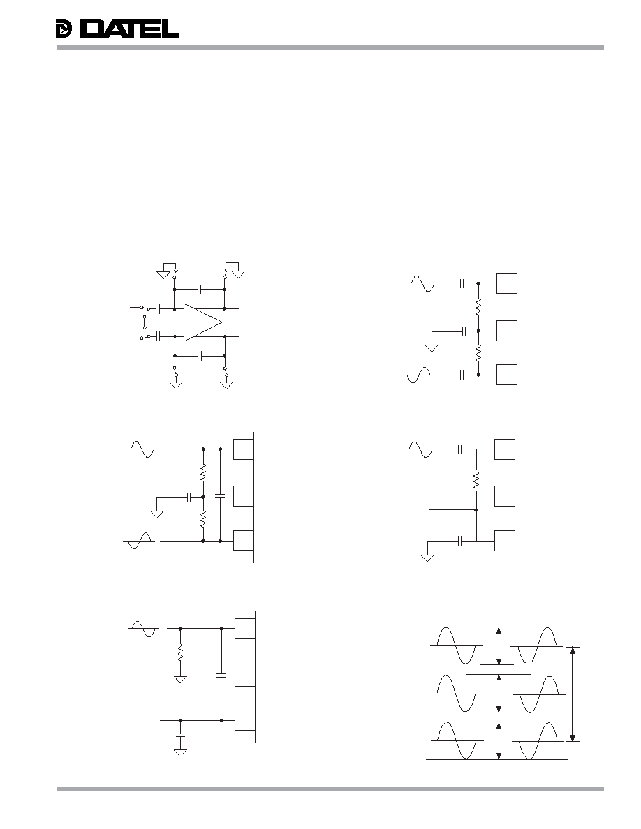
Differential Analog Input
The analog input is a differential input that can be configured in
various ways depending on the signal source and the level of
performance desired. A fully differential connection as shown
in figures 3.2 and 3.3 will give the best performance.
The ADS-235, ADS-236 and ADS-237 are powered by a single
+5V analog power supply which limits the analog input to
between ground and +5V. For the differential input connection
this implies that the analog input common mode voltage can
range from 1.0V to 4.0V, see figure 3.6. Performance for the
converter does not change significantly with the value of the
analog input common mode voltage. A DC voltage source, V
DC
,
equal to 2.3V, typical, is provided to help simplify circuit design
when using an AC coupled differential input. This low
impedance voltage source is not designed to be a reference
voltage but makes an excellent DC bias source. This bias
voltage source stays well within the analog input common
mode voltage range over temperature.
The difference between the converter's two internal reference
voltages is 2V. For the AC coupled differential input, figure 3.2,
if V
IN
is a 2Vp-p sinewave with ≠V
IN
180 degrees out of phase
with V
IN
, then V
IN
+ is a 2Vp-p sinewave riding on a DC bias
voltage equal to V
DC
. Consequently, the converter will be at a
positive full scale when the V
IN
+ input is at V
DC
+1V and the
V
IN
≠ input is at V
DC
-1V (V
IN
+ - V
IN
≠ = 2V). Conversely, the ADS
will be at negative full scale when the V
IN
+ input is equal to
V
DC
-1V and V
IN
≠ is at V
DC
+1V (V
IN
+ - V
IN
≠ = ≠2V). Thus, the
converter has a peak-to-peak differential analog input voltage
range of ±2V.
The analog input can be DC coupled, figure 3.3, as long as the
inputs are within the analog input common mode voltage range
(1.0V
£
V
DC
£
4.0V). The resistors, R, are not absolutely
necessary but may be used as load setting resistors. A
capacitor, C, connected from V
IN
+ to V
IN
≠ will help filter high
frequency noise. Values of approximately 20pF are normally
sufficient but the actual value must take into account the
highest frequency component of the input signal.
Single-Ended Analog Input
The circuit in figure 3.4 may be used with a single-ended AC
coupled input. Assuming again that the difference between the
two internal voltage references is 2V and V
IN
is a 4Vp-p
sinewave, then V
IN
+ is a 4Vp-p sinewave riding on a positive
voltage equal to V
DC
. The converter will be at a positive full
scale when V
IN
+ is at V
DC
+2V (V
IN
+ - V
IN
≠ = 2V) and will be
equal to a negative full scale when VIN+ is equal toVDC-2V
(V
IN
+ - V
IN
≠ = ≠2V). In this case, V
DC
could range between 2V
and 3V without significant change in the converters
performance. The simplest way to obtain a V
DC
voltage is to
use the V
DC
output provided by the converters.
The single-ended analog input can be DC coupled, as shown
figure 3.5, as long as the input is within the analog input
common mode voltage range. The resistor, R, shown is not
absolutely necessary but may be used as a load setting
resistor. A capacitor, C, connected between V
IN
+ and V
IN
≠ will
help filter high frequency noise. A value of approximately 20pF
is normally sufficient but the actual value must take into
account the highest frequency component of the input signal.
INTERNAL REFERENCE GENERATOR, VR
OUT
VR
IN
The ADS-235/236/237 have an internal reference generator,
therefore, an external voltage is not required. V
ROUT
must be
connected to V
RIN
when using the internal reference voltage.
Two reference voltages are generated internally, 1.3V and
3.3V, for a fully differential input range of ±2V.
An external reference may be used by connecting the external
voltage reference to the V
RIN
pin with V
ROUT
left open. These
units are tested with V
RIN
equal to 3.5V.
In order to minimize overall converter noise it is recommended
that adequate high frequency decoupling be provided at the
V
RIN
pin.
Digital I/O and Clock
The ADS-235, ADS-236 and ADS-237 provide a standard
high-speed interface to external TTL/CMOS logic families. In
order to ensure rated performance the duty cycle of the clock
should be held at 50% ±5%, have low jitter and operate at
standard TTL levels. Performance is guaranteed for conversion
ADS-235, ADS-236, ADS-237
5
Æ
Æ
rates above 0.5MHz in order to ensure proper performance of
the internal dynamic circuits.
Power Supplies and Grounding
The ADS-235, ADS-236 and ADS-237 have separate digital
and analog power supply pins and grounds (refer to the Input/
Output Connections table for pin numbers) to reduce digital
noise in the analog signal path. The digital data outputs also
have a separate supply pin, +DV
S
2, which can be powered
from either a 3.0V or 5.0V supply to allow the user the option
of interfacing with 3.0V logic.
The converters should be mounted on a board that provides
separate low impedance paths for the analog and digital
supplies and grounds. For best performance the supplies used
should be clean, linear regulated supplies. All power supplies
should be bypassed to ground with a 10uF tantalum capacitor
in parallel with a 0.1uF ceramic capacitor. Locate the bypass
capacitors as close to the converter as possible. If the converter
is to be powered from one supply then the analog supply and
ground pins should be isolated with ferrite beads from the
digital supply and ground pins. See the Typical Connection
Diagram, Figure 4.
In order to minimize overall converter noise it is recommended
that the V
RIN
pin be bypassed using a 4.7 uF tantalum capacitor
in parallel with a 0.01 uF ceramic capacitor. Locate the bypass
capacitors as close to the unit as possible.
Figure 3.1 Analog Input Sample-and-Hold
Figure 3.2 AC Coupled Differential Input
Figure 3.4 AC Coupled Single Ended Input
Figure 3.3 DC Coupled Differential Input
Figure 3.5 DC Coupled Single Ended Input
Figure 3.6 Differential Analog Input Common
Mode Voltage Range
Figure 3. Analog Input
C
H
V
IN
+
V
IN
≠
V
OUT
≠
V
OUT
+
C
H
≠ +
+ ≠
ÿ1
ÿ1
ÿ1
ÿ1
ÿ1
ÿ1
ÿ2
C
S
C
S
8
10
9
≠V
IN
R
V
IN
R
V
IN
+
V
IN
≠
V
DC
8
10
9
R
R
C
V
IN
≠V
IN
V
DC
V
DC
V
IN
+
V
IN
≠
V
DC
8
10
9
R
V
IN
+
V
IN
≠
V
DC
V
IN
V
DC
8
10
9
C
R
V
IN
+
V
IN
≠
V
DC
V
DC
V
DC
V
IN
V
IN
+
V
IN
+
V
IN
+
V
IN
≠
V
IN
≠
V
IN
≠
+5V
C
o
m
m
on
M
o
de V
o
l
t
age
R
a
nge
2.0Vp-p
2.0Vp-p
2.0Vp-p
V
DC
=+4.0V
V
DC
=+1V
0V
+1.0<V
DC
<+4.0V