 | –≠–ª–µ–∫—Ç—Ä–æ–Ω–Ω—ã–π –∫–æ–º–ø–æ–Ω–µ–Ω—Ç: PC-430F | –°–∫–∞—á–∞—Ç—å:  PDF PDF  ZIP ZIP |
Æ
Æ
FEATURES
∑∑
∑∑
∑
Up to 10 MHz A/D sample rate
∑∑
∑∑
∑
Choice of 12, 14, or 16-bit A/D resolution
∑∑
∑∑
∑
Up to 8 Mb dual-ported RAM
∑∑
∑∑
∑
Analog pretrigger ring buffer
∑∑
∑∑
∑
8k x 32 expansion RAM
∑∑
∑∑
∑
Programmable interrupt to PC/AT host
∑∑
∑∑
∑
2-16 Channel simultaneous sampling eliminates
phase skew
∑∑
∑∑
∑
On-board 320C30 40 MHz digital signal processor
∑∑
∑∑
∑
On-board DSP library - FFT's, filters, matrix math,
floating point, etc.
∑∑
∑∑
∑
Fast, simple, powerful command executive. No local
programming required.
∑∑
∑∑
∑
Windows
Æ
compatible
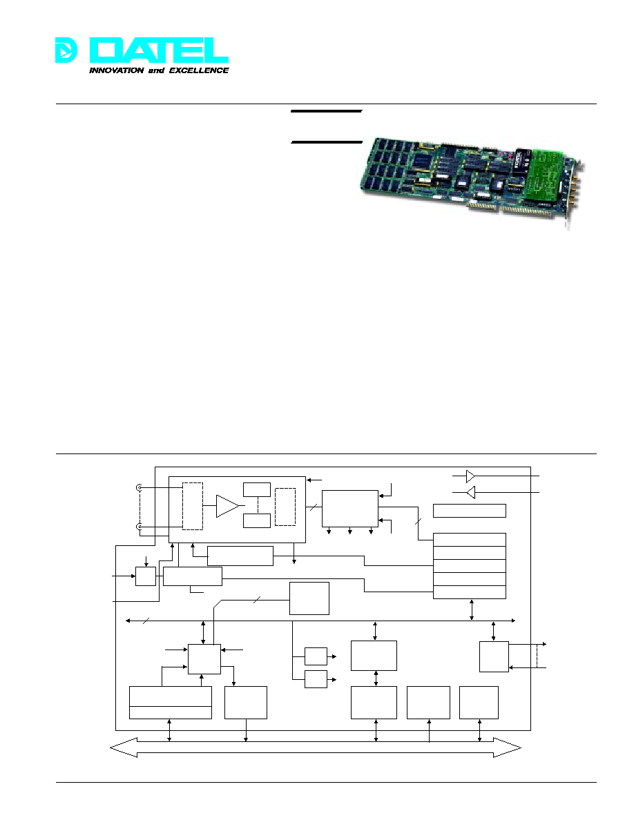
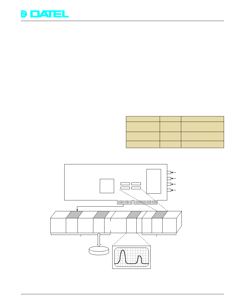
Advanced performance from the PC-430's on-board Digital
Signal Processor (DSP) offers a broad range of high-speed
waveform analysis and recording applications. The PC-430 will
acquire up to sixteen analog input channels, digitize and store
them in local memory while DSP math processing and data
transfer are done concurrently. The system is intended for
preprocessing "seamless" A/D data streams to mass storage.
The PC-430 is ideal for non-stop, continuous Fast Fourier
Transform (FFT) processing, communications receiver signal
collection to disk, or simultaneous graphics display of spectral
data. Application areas include signal recovery from noisy
channels, harmonic distortion analyzers, and vibration/
resonance filtering systems. For use with ultrasonic, sonar, or
Figure 1. Functional Block Diagram
PC-430
Very High Speed ISA
A/D-DSP Coprocessor Board
acoustic signals, the interrupt-driven, simultaneous block
transfers of data ensure no information loss. Other uses
include high-speed mapping and imaging, satellite channels,
astrophysics, seismology, biomedical signals, array
processing, control systems, simulators, engine analyzers,
aerodynamics, and vehicle systems.
Several different "pluggable" analog options offer up to 16 input
channels in single-ended or differential configurations, multiple
input ranges, sampling rates to 10 MHz, 12/14/16-bit A/D
resolutions, and various simultaneous sampling configurations
(1 A/D per channel) up to 16 channels. The simultaneous
feature is intended for parallel sampling applications that cannot
tolerate phase skew introduced by the A/D system.
A/D triggering uses a programmable timer-counter section
which controls the interval between A/D conversions and the
interval between multi-sample A/D scans. The number of
samples can be counted for repeating array sampling. The
timer-counter uses an on-board crystal oscillator or an
Channel Address
Counter
FIFO
Memory
2k to 8k
samples
Empty Half
Full
Analog
Input
Channels
320C30
DSP
82C54
Timer/Counter
External
Trigger
32 bit
Data
40MHz
Command/ Status
Interrupt
to PC
32 to 16-bit
Transceivers
DC/DC
Power
Converter
Bus
Interface
ISA Bus
Local DSP Bus
+5V
SSH Control
Hold
RST
Interrupt
TMR 0
Dual
Port
RAM
FIFO Data
FIFO Flag
Start Channel Address
Command Register
Timer/Counter
DSP
I/O
Map
Expansion
Memory
8k x 32
External
Start Clock
10MHz
Expansion Connectors
RS-232
Serial Port
I/O Map
Reset
Trig.
Sel.
Int. Trig.
EOC
32
512kb to 8Mb
Analog Outputs
and Comparators
D/A
D/A
Parallel
I/O
82C55
24-bit
Digital
I/O
32
bank
sw
M
U
X
A/D
A/D
C
T
L
Memory Base Address
and Page Register
Pluggable Analog Section
Now with
LabVIEW
Æ
VI's
NEW
DATEL, Inc., Mansfield, MA 02048 (USA)
∑
Tel: (508)339-3000, (800)233-2765 Fax: (508)339-6356
∑
Email: sales@datel.com
∑
Internet: www.datel.com
95
PC-430
Æ
Æ
DATEL, Inc., Mansfield, MA 02048 (USA)
∑
Tel: (508)339-3000, (800)233-2765 Fax: (508)339-6356
∑
Email: sales@datel.com
∑
Internet: www.datel.com
external timebase for precision phase-tracking. The digital
output of the A/D passes directly to a first-in, first-out (FIFO)
memory. The FIFO acts to decouple the precision timing of
the A/D section with the block transfers governed by the DSP.
Additional internal DSP timers are also used.
A/D FIFO data may be sent to dual port random access
memory (DPR) shared with the host PC/AT bus. The DPR is
organized as 128k by 32 bits up to 2M x 32. Typically, a
swapped dual buffer method is used so that samples are not
lost during other processing. Local hardware registers control
all A/D, FIFO, and trigger activity.
Single cycle fetch and execution, parallel instructions, zero-
overhead of looping instructions, software variable wait states,
block repeat and a 64-word internal instruction cache memory are
some of the advanced high speed features of the Texas
Instrument 320C30 DSP. The DSP uses 32-bit local data paths for
very high speed. Data passed to the host PC/AT bus uses 32-to-
16 bit transceivers to the DPR. Simultaneous access attempts to
the DPR by both the PC/AT host and the DSP are resolved by
high speed arbitration logic. The DSP also has a separate 8k by
32-bit local expansion memory for the stack or temporary data.
The architecture of the DSP allows simultaneous processing of
two tables from two sections of memory.
The PC-430 appears as both I/O and memory addresses to
the host PC/AT. At power up, the PC-430 is disconnected
from host memory and must be enabled through the I/O
registers. The DPR may be addressed up to 16 Mb.
After loading in the Executive from disk to the DPR, the DSP
is transitioned from reset to run using an I/O control bit. The
board may be reset at any time using this technique. The
comprehensive Executive software package offers fast A/D
sample collection and DSP math without writing any local
programs. A simple, powerful, high speed command list is
used to access the local DSP library.
Host PC to PC-430 Interface
The DPR can be accessed from the PC through two user-
selectable methods, both of which map the DPR into the PC's
memory. The first method locates a movable 1 MB window of
DPR into the PC's extended memory above the 1 MB address.
The host PC must have at least 1 MB of free extended memory
below the PC's 16 MB address. Since the host PC memory is
usually contiguous, this means the PC cannot have more than
15 MB of memory using this first method. Also, the CPU must
be in protected mode to access this PC-430 extended memory.
PC-430 software uses XMS drivers for this purpose.
The second method is new to the enhanced PC-430. This
method maps a 64 kB DPR relocatable window into the PC's
memory anywhere below the 16 MB address. Usually in this
"paged" mode, the 64 kB block will be located below 1 MB
where the CPU can access it in real mode. DPR blocks
longer than 64 kB are accessed by a sliding window technique
controlled by an I/O mapped paging register. Either access
method works with DOS or Windows and both have speed
and software trade-offs.
Memory Organization
At power up, the entire PC-430 DSP memory is empty (there
is no local non-volatile memory). All executable code is
downloaded from the host PC disk into the PC-430's Dual Port
RAM (DPR). Typically, this download is from a TI COFF object
file. The host PC does not require any extended memory to
be installed for the PC-430 but any existing PC extended
memory may be used to collect PC-430 data blocks.
PC-430 SOFTWARE
The following are some methods to control the PC-430:
∑ Use the PC-430 DATEL Executive software
∑ Modify the Executive by adding your own code.
∑ Develop your application from scratch using the TI compiler.
∑ PC-430LV "bridge" drivers to National Instruments LabVIEW.
PC-430EXEC - Executive, Commander, and Scheduler
DATEL's Executive software offers an easy way to control the
PC-430 which retains the full power of the DSP. The Executive
consists of two portions - a host side menu-driven user
interface (the Commander) and a local downloaded DSP
executable code (the Scheduler). The Commander is
provided either in an MS-DOS graphics version or compatible
to Microsoft Windows. When the Commander is invoked, it
performs a DPR memory test, loads the scheduler into the
DPR and waits for user-directed control of the PC-430.
The Executive can perform three tasks simultaneously at high
speed without losing data:
∑ Fast "seamless" non-stop A/D data collection to local DSP
memory.
∑ Concurrent DSP math processing of data blocks.
∑ Simultaneous upload of processed data blocks to the PC host.
The Commander is primarily a high speed data acquisition
recorder plus user interface. The PC-430 generated data can
be sent to host PC memory or disk. The saved disk files can
then be displayed and processed by any graphics system
such as a spreadsheet which accepts binary or floating point
files. Commander operation may be batched to interleave
external functions between data saves.
The scheduler is a binary COFF file (SKED.OUT) which
consists of local DSP boot code, vectors, local interrupt service
routines (ISR's), the full DSP library, software control/status
blocks and the Application Function Block (AFB) processor.
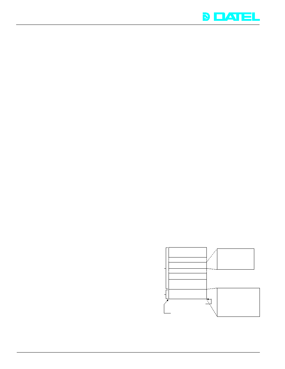
Figure 2. Local DSP Map
Local DSP Memory Map
DSP Registers and
Internal 2k x 32 RAM
Control Registers
8k x 32 Expansion RAM
Optional
additional memory
Shared dual access
memory, 128k x 32
82C55 Dig. I/O
FIFO A/D Data
Start Channel Address
Command Register
82C54 Counter/Timer
1.5 - 8Mb
Data buffers
DSP library
Application Function Block
Buffer map
Control/status
Monitor/Debugger
Interrupt vectors
DSP location 0
Relocatable MEMBASE
location in host PC
512kb window
to host PC
no host
PC access
96
PC-430
Æ
Æ
DATEL, Inc., Mansfield, MA 02048 (USA)
∑
Tel: (508)339-3000, (800)233-2765 Fax: (508)339-6356
∑
Email: sales@datel.com
∑
Internet: www.datel.com
FUNCTIONAL SPECIFICATIONS
(Typical at +25 ∞C, dynamic conditions, gain = 1, unless noted)
PC-430F
2 Simultaneous
(two A/D's)
Single Ended
0 to +10 V
±5 V
±15 V
2 µs
--
1 K
165 ns
20 ns
±40 ps
12 bits
400 ns [Note 12]
±1
±1
±0.1
±0.1
2 MHz
2 MHz/chan.
(2 chans.)
≠70 dB
PC-430E
16SE/8D [Note 8]
(single A/D)
SE or Diff.
0 to +10 V
±10 V
±5 V
±15 V
2 µs
±10 V
100 M
750 ns
20 ns
±40 ps
12 bits
500 ns
±1
±0.75
±0.1
±0.1
2 MHz
500 kHz
[Note 4]
≠72 dB
PC-430B
4
(single A/D)
Single Ended
0 to +10 V
±10 V
±5 V
±15 V
2 µs
--
10 M
750 ns
20 ns
±100 ps
14 bits
1.6 µs
±1.5
±1
±0.3
±0.3
500 kHz
330 kHz
≠75 dB
ANALOG INPUTS
Number of Channels
Input Configuration
(non-isolated) [Note 19]
Full Scale Input Ranges
(user-selectable) (gain = 1)
[Notes 1 & 16]
Input Overvoltage
(no damage, power on)
Overvoltage Recovery
Time, maximum
Common Mode Voltage
Range, maximum
Input Impedance [Notes 6 &10]
Acquisition Time
Aperture Delay
Aperture Delay Uncertainty
Resolution
Conversion Period
Integral Non-linearity
(LSB of FSR)
Differential Non-linearity
(LSB of FSR)
Full Scale Temperature
Coefficient (LSB per ∞C)
Zero or Offset
Temperature Coefficient
(LSB per ∞C)
Throughput to FIFO
(single channel, gain = 1)
Throughput to FIFO
(multiple channels, gain = 1)
Total Harmonic Distortion
[Note 3]
PC-430D
1
(single A/D)
Differential
±5 V
±15 V
2 µs
±1 V
2 K
50 ns
10 ns
±7 ps
12 bits
200 ns
±2
±1
±0.1
±0.3
5 MHz
[Note 15]
≠68 dB
SAMPLE/HOLD
A/D CONVERTER
SYSTEM DC CHARACTERISTICS [Note 7]
SYSTEM DYNAMIC PERFORMANCE [Note 2]
ANALOG INPUTS
Programmable Gains
See Note 1
Common Mode Rejection
(DC - 60 Hz)
-80 dB (g = 100) (430E)
Addressing Modes
1. Single channel
2. Simultaneous sampling
3. Sequential with
autosequenced addressing
4. Random addressing by host
software
A/D CONVERTER
Output Coding
Positive-true, right justified,
straight bin. (unipolar) or right-
justified 2's complement
(bipolar) with sign extension
thru bit 15
Trigger Sources
1. Local Pacer frame clock
(Software selectable)
2. External TTL frame clock
3. Analog threshold comp.
A/D Sample Clock
1. Internal programmable
(software selectable)
82C54 timer
2. Ext. TTL input, active low
Please read all notes carefully.
The PC-430J in short-cycled addressing is recommended in place of the PC-430A. Model PC-430E can substitute for the PC-430C.
97
PC-430
Æ
Æ
DATEL, Inc., Mansfield, MA 02048 (USA)
∑
Tel: (508)339-3000, (800)233-2765 Fax: (508)339-6356
∑
Email: sales@datel.com
∑
Internet: www.datel.com
ANALOG INPUTS
Number of Channels
Input Configuration
(non-isolated) [Note 19]
Full Scale Input Ranges
(user-selectable) (gain = 1)
[Notes 1 & 16]
Input Overvoltage
(no damage, power on)
Overvoltage Recovery
Time, maximum
Common Mode Voltage
Range, maximum
Input Impedance [Notes 6 &10]
Acquisition Time
Aperture Delay
Aperture Delay Uncertainty
Resolution
Conversion Period
Integral Non-linearity
(LSB of FSR)
Differential Non-linearity
(LSB of FSR)
Full Scale Temperature
Coefficient (LSB per ∞C)
Zero or Offset
Temperature Coefficient
(LSB per ∞C)
Throughput to FIFO
(single channel, gain = 1)
Throughput to FIFO
(multiple channels, gain = 1)
Total Harmonic Distortion
[Note 3]
FUNCTIONAL SPECIFICATIONS
(Typical at +25∞C, dynamic conditions, gain = 1, unless noted)
PC-430K
2 Simultaneous
(two A/D's)
Limited Differential
0 to +10 V, ±5 V
(separate models)
±15 V
--
±1 V
1 K
50 ns
10 ns
±7 ps
12 bits
200 ns [Note 12]
±2
±1
±0.1
±0.3
5 MHz
5 MHz/ch.
≠68 dB
PC-430G
2 Simultaneous
(two A/D's)
Single Ended
±5 V or
0 to +10 V
(separate models)
±15 V
2 µs
--
1 M
350 ns [Note 11]
20 ns
±70 ps
14 bits
500 ns [Note 12]
±1.5
±1
±0.3
±0.3
1 MHz
1 MHz/chan.
(2 chans.)
≠80 dB
PC-430H
1
(single A/D)
Differential
±5 V
±15 V
1 µs
±1 V
2 K
35 ns
±10 ns
3 ps rms
12 bits
100 ns
±1.5
±1
±1
±1
10 MHz
[Note 15]
≠65 dB
PC-430J
8 Simultaneous A/D's
[Note 8]
Single Ended
±5 V, ±10 V
[Note 13]
±15 V
3 µs
--
8 K
(bipolar)
400 ns
--
--
12 bits
2 µs [Note 12]
±1
±1
[Note 13]
[Note 13]
400 KHz
250 KHz/chan.**
≠75 dB
SAMPLE/HOLD
A/D CONVERTER
SYSTEM DC CHARACTERISTICS [Note 7]
SYSTEM DYNAMIC PERFORMANCE [Note 2]
**A 380 KHz per channel option is available on special order.
NOTES
1.
Resistor-programmed gain from x1 to x100 is available on
PC-430E with increased settling delay at higher gain.
2.
Total throughput for single A/D modules includes MUX settling time
after changing the channel address, S/H acquisition time to rated
specifications, A/D conversion, and FIFO transfer. Total throughput
is not delayed by host software whenever the FIFO is not full.
3.
THD test conditions are:
A. Input freq.
500 KHz (430F)
200 KHz (430B,E,G)
50 KHz (430J,L,M)
1 MHz (430D,K,N,P)
2 MHz (430H)
B. Generator/filter THD is -90 dB minimum.
C. THD computed by FFT to 5th harmonic.
( V2
2
+ V3
2
+ V4
2
+ V5
2
)
0.5
Vin
D. Inputs are half full scale less 0.5 dB. No channel advance.
E. A/D sample rate = 500 kHz (430B,E,G), 4 MHz (430D,K),
2 MHz (430F), 10 MHz (430H), 250 kHz (430J), 190 kHz (430L,M),
2.5 MHz (430P)
4.
The rates shown for sequential sampling with single A/D modules
are the maximum A/D converter start rates and include MUX
sequencing and settling. For example, if four channels of the
PCI-430E were scanned, the maximum sample rate on any one
channel would be 2 µs x 4 channels = 8 µs (125 KHz per channel).
log10
(
)
THD = 20
98
PC-430
Æ
Æ
DATEL, Inc., Mansfield, MA 02048 (USA)
∑
Tel: (508)339-3000, (800)233-2765 Fax: (508)339-6356
∑
Email: sales@datel.com
∑
Internet: www.datel.com
FUNCTIONAL SPECIFICATIONS
(Typical at +25∞C, dynamic conditions, gain = 1, unless noted)
ANALOG INPUTS
Number of Channels
Input Configuration
(non-isolated) [Note 19]
Full Scale Input Ranges
(user-selectable) (gain = 1)
[Notes 1 & 16]
Input Overvoltage
(no damage, power on)
Overvoltage Recovery
Time, maximum
Common Mode Voltage
Range, maximum
Input Impedance [Notes 6 &10]
Acquisition Time
Aperture Delay
Aperture Delay Uncertainty
Resolution
Conversion Period
Integral Non-linearity
(LSB of FSR)
Differential Non-linearity
(LSB of FSR)
Full Scale Temperature
Coefficient (LSB per ∞C)
Zero or Offset
Temperature Coefficient
(LSB per ∞C)
Throughput to FIFO
(single channel, gain = 1)
Throughput to FIFO
(multiple channels, gain = 1)
Total Harmonic Distortion
[Note 3]
PC-430L
16 Simultaneous
A/D's [Note 8]
Single Ended
±5 V, ±10 V,
(user selectable)
[Note 13]
±15 V
--
--
8 K
400 ns
--
--
12 bits
2 µs [Note 12]
±2
±1
[Note 13]
[Note 13]
400 kHz
190 kHz/chan.
-75 dB
PC-430M
4 Simultaneous
A/D's
Single Ended
±10 V
±12 V
--
--
10 M
--
--
--
16 bits
5 µs [Note 12]
±4
±3
±1
±1
200 KHz
200 KHz/chan.
-83 dB
PC-430P
4 Simultaneous
A/D's
Single Ended
±2.5 V or
0 to +5 V
(user selectable)
±7 V
--
--
1000
--
--
--
14 bits
400 ns [Note 12]
±3
±1.5
±0.5
±0.5
3 MHz* min.
[Note 9]
2.5 MHz/chan.
-75 dB
PC-430N
2 Simultaneous
A/D's
Single Ended
±2.5 V
±15 V
--
--
10 M
or 50
35 ns
±10 ns
5 ps
14 bits
200 ns [Note 12]
±1
±1
±0.5
±0.5
5 MHz
5 MHz/chan.
-75 dB
SAMPLE/HOLD
A/D CONVERTER
SYSTEM DYNAMIC PERFORMANCE [Note 2]
SYSTEM DC CHARACTERISTICS [Note 7]
5.
For fastest response on the analog comparator trigger, keep the
reference voltage near the trip input voltage. To avoid overload
recovery delays, do not let the trip input (or any other analog input)
exceed ±10V.
6.
The input impedance of 10 M
minimum avoids attenuation errors
from external input source resistance. For many applications, an in-
line coaxial 50
shunt, inserted adjacent to the front connectors, is
recommended to reduce reflections and standing wave errors.
7.
Allow 20 minutes warmup time to rated specifications for models
PC-430B,G,M,N.
8.
A 25-pin DB-25S connector is used for the PC-430E, J, and L.
9.
The sample rate to published specifications is 3 MHz. The A/D is
functional to 5 MHz. Data output is delayed by 4 sample clocks.
Data output is pipelined meaning that the first four samples should
be discarded. The design is intended for semi-continuous
sampling of wideband signals. Approximately 5 dB SFDR
improvement can be achieved by directly connecting an external
A/D sample clock. Contact DATEL for details.
10.
Input impedance is shown with power on. Impedance with power
off is 1.5 K
or less.
11.
PC-430G acquisition time is 350 ns to ±0.01% of FSR.
12.
All channels in simultaneous sampling.
* The sample rate to published specifications is 3 MHz. The A/D is functional to 5 MHz. Valid data output per channel is delayed by 4 samples after the
start of the sample clock. Please make note of this for products such as the PC-414P, PC-430P, and DVME-614P which use non-continuous A/D
sampling. Data output is pipelined meaning that the first four samples per channel should be discarded. For all 4 channels, discard 16 samples. The
design is intended for semi-continuous sampling of wideband signals and is less suitable for low speed data acquisition. Approximately 5 dB SFDR
improvement can be achieved by directly connecting an external A/D sample clock. Contact DATEL for details.
99
PC-430
Æ
Æ
DATEL, Inc., Mansfield, MA 02048 (USA)
∑
Tel: (508)339-3000, (800)233-2765 Fax: (508)339-6356
∑
Email: sales@datel.com
∑
Internet: www.datel.com
SPECIFICATIONS, CONTINUED
(Typical @ +25∞C, dynamic conditions, unless noted)
TRIGGER CONTROL
Programmable Timer
Counter Type
82C54 (DSP waits required)
Functions
1. EOC sample counter.
2. A/D start rate (16 bit divisor)
3. SSH sample counter (430A)
Pacer Sample Counter
3 to 65,535 samples.
Clock Source
Internal
10 MHz crystal clock
External
TTL input, direct to A/D
Analog Trigger
Uses comparator and on-
board D/A channel. [Note 5]
Pretrigger
Sample down counter is
delayed until an external
trigger. Pretrigger samples
are stored in a ring buffer.
Architecture
I/O and memory mapped,
for IBM-PC/AT, and
compatibles.
I/O Mapping
Three 16-bit I/O registers.
Decodes I/O address lines
A9 - A2.
Data Transfer
Memory block transfer, real
or protected mode.
Data Bus
16 bits
Number of Interrupts
1 interrupt, software
selectable on levels 9, 10,
11, or 15.
Bus Interrupt Sources
DSP interrupt request to PC.
CPU Type
TI TMS 320C30
Local Data Bus
32 bits
CPU Clock Speed
40 MHz
Local DMA Controller
Internal to 320C30 CPU
Primary Memory
(Dual access to PC/AT)
128k x 32 static RAM,
expandable to 2048k x 32
total (8 Mb).
Expansion Memory
8k x 32 static RAM
Internal DSP Memory
Two 1k x 32
Dual Port Access
Hold mode by control bit or
from PC/AT dynamic hold
per each access.
CPU Test Port
Supports TI XDS1000
Extended Development
System
Local Interrupts to DSP
Int 0-3 from PC host
request, A/D FIFO or acquire
flags or optional external
interrupt.
DSP Wait States
Software programmable up
to 7 waits via DSP register.
Digital I/O Port
24 lines, programmable In
or Out, TTL levels, 82C55
MISCELLANEOUS
Analog Input Connectors
Four miniature threaded
coaxial, type SMA, mounted
on rear slot. DB-25 for
PC-430E,J, & L.
Trigger Connector
(all models except E, J, & L)
5th SMA for external TTL
trigger.
D/A Analog Outputs
2 channels, ±5V or ±10V
output ranges, 12 bit
resolution, 5µs settling. May
be used to select analog
trigger level.
A/D FIFO Memory
2048 or 8192 A/D samples,
programmable 16 or 32 bits
wide.
Memory Expansion Port
Dual-row header connector
for 320C30 memory
(unbuffered).
Serial Port and External
Trigger/Pacer Clock
Two serial channels,
(dual row header)
compatible to 320C30 serial
ports. Both scan (Trigger)
and A/D sample clocks are
accepted at connector.
RS-232-C Serial Port
3 header pins. Uses
software UART.
Operating Temp. Range
0 to +60∞C
Storage Temp. Range
-25 to +85∞C
Humidity
10% to 90%,
non-condensing.
Altitude
0 to 10,000 feet. Forced
cooling is recommended.
Power Required
+5V DC 3.5 Amps max.
Outline Dimensions
4.5 x 13.2 inches
ISA BUS INTERFACE
LOCAL MICROCOMPUTER
13.
PC-430J and L bipolar input is user-selectable ±5 V or ±10 V per
channel (default). Total full scale error over temperature range is
±4 LSB maximum. Total zero/offset error over temperature range
is ±2 LSB maximum. Monotonicity: no missing codes over
temperature range.
14.
Avoid mixing external triggers which are a close submultiple of the
internal A/D start clock to prevent lost samples.
15.
Models PC-430D and H use a single channel 12-bit A/D converter
with ±5 V inputs. An external A/D clock is required above 4 MHz
and the 82C54 timer must be bypassed. 10 MHz sampling may
continue until the FIFO memory is full.
16.
Input polarity: Some models are fixed as bipolar only whereas
others are user-selectable unipolar or bipolar. Still others require
separate model numbers.
17.
Models F, G, J, K, L, M, N, and P use one A/D converter per channel.
18.
The customer must use shielded cables to insure EMC compliance.
19.
A/D-per-channel boards (models F, G, J, K, L, M, N, P) may be
operated in "software differential" mode. Two A/D's are applied to the
high and low legs of a single differential input channel. The two data
values are then algebraically subtracted, either on the fly in real time or
after all samples have been stored. Channel capacity in "software
differential" is one-half the number of single-ended channels.
This technique offers excellent bandwidth, high common mode
rejection and optional mix of single-ended and differential channels.
100
PC-430
Æ
Æ
DATEL, Inc., Mansfield, MA 02048 (USA)
∑
Tel: (508)339-3000, (800)233-2765 Fax: (508)339-6356
∑
Email: sales@datel.com
∑
Internet: www.datel.com
Application Function Blocks (AFB)
The Executive optimizes three competing objectives:
∑ Easy to use
∑ Fast
∑ Powerful (access to a full DSP software library)
A high speed command list is used to achieve these mutually
exclusive goals. The AFB is a short list of commands which
call local PC-430 DSP library functions previously downloaded
by the Commander to the DPR and reside in the scheduler.
No local programming is needed.
Similar to a spreadsheet macro or DOS batch file but much
faster, the user writes the AFB file with any text editor and the
Commander converts it on the PC side to an internal binary
form. The Commander then downloads the converted AFB
file to the DPR for execution.
The AFB is powerful because of full access to the DSP library
and because repeating functions may be looped. These loops
in turn may be nested. Loops can run with a loop count or
"forever". Unlike a slow ASCII interpreter, the AFB system
runs at nearly the full speed of the 320C30 DSP with minimal
overhead. Besides the large DSP library, the user may write
additional AFB functions in "C" or TI assembly and integrate
them with the schedular.
AFB Library Functions
Over 60 functions are included in the Executive AFB library.
These are fully described in the PC-430 User's Manual
(included with the board). The functions become resident
when the scheduler is downloaded. Fully commented source
code to these functions is found in the PC-430SRC and
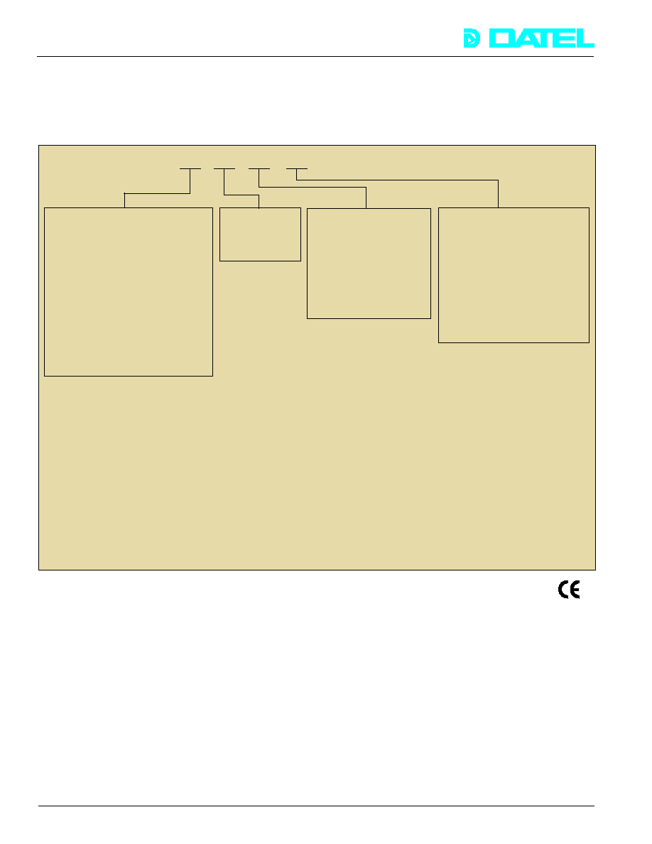
Figure 3. Array Preprocessing
DSP
512kb SRAM
Memory
MUX
A/D
PC-430
Analog
Inputs
430
ISR
DISK
BUF
640kb
VID
RAM
ROM
DPR
Commander
Display
Base Memory
Host
Memory
DATA RDY INTRPT
Extended Memory or
64kb in base memory
PC-430WINS packages. Most functions are written in a mix
of high performance "C" and 320C30 Assembly language.
Users may modify the functions or add their own functions
and rebuild the system.
The functions are grouped in five major categories:
∑ A/D Scan and Timer/Counter Routines
∑ DSP Array Math Routines
∑ Array Conversion Routines
∑ Single Variable Transcendentals
∑ Buffer Management
FIFO Data Format
A/D data is delivered as a stream from the FIFO memory. For
multichannel inputs, this means that data is multiplexed. For
example, for 4-channel inputs, the output channel sequence is
0, 1, 2, 3, 0, 1, . . . Some applications may need this data de-
multiplexed by software so that each channel's data is placed
in its own separate buffer.
Table 1. PC-430 I/O Registers
I/O Address
Direction
Function
I/O BASE + 0
Write
PC Command Register
Read
PC Status Register
I/O BASE + 2
Write
Memory Base Address
Read
Not Used
I/O BASE + 4
Write
Page Address Register
101
PC-430
Æ
Æ
DATEL, Inc., Mansfield, MA 02048 (USA)
∑
Tel: (508)339-3000, (800)233-2765 Fax: (508)339-6356
∑
Email: sales@datel.com
∑
Internet: www.datel.com
Input Channels, A/D Resolution
B = 4SE chans., 14 bits
D = 1D chan., 12 bits
E = 16SE/8D chans., 12 bits
F = 2SE simul. chans., 12 bits
G = 2SE simul. chans., 14 bits
H = 1D chan., 12 bits
J = 8SE simul. chans., 12 bits
K = 2SE simul. chans., 12 bits
L = 16SE simul. chans., 12 bits
M = 4SE simul. chans., 16 bits
N = 2SE simul. chans., 14 bits
P = 4SE simul. chans., 14 bits
A/D FIFO Size
1 = 2k samples
2 = 8k samples
A/D Polarity
A = Bipolar or selectable
B = Unipolar
For models with user-
selectable polarity use the
"A" designator. CAUTION:
Read the input range
specifications carefully.
PC-430
ORDERING INFORMATION
Each board is power-cycle burned-in, tested and calibrated. All models include a user's manual. The warranty period is one
year.
61-7342340
SMA to BNC cable, one required per channel, one meter.
Software:
PC-430EXEC
Executive, Commander, and Scheduler executables only for MS-DOS. 3.5 inch 1.4 Mb disks.
PC-430SRC
Full source code to PC-430EXEC. Requires Microsoft and TI "C". Includes MS-DOS Window Boss
library.
PC-430WIN
Microsoft Windows 95 version of PC-430EXEC. Executables only.
PC-430WINS
Full source code to PC-430WIN. Requires Microsoft Visual BASIC, Borland C++, MASM, and TI "C".
PC-430LV, LVS
Bridge driver to National Instruments' LabVIEW
Æ
. See PC-430LV data sheet.
UM-CMDRSRC
Commander software manual (included with Commander).
Example: PC-430G2A 14 bits, 8k FIFO, bipolar input, 512 kB memory.
Pentium is an Intel trademark
Windows and MS-DOS are Microsoft trademarks
LabVIEW is a National Instruments trademark
IBM is a trademark of the IBM Corp.
Hardware:
Total On-Board Memory*
1 = 512 kilobytes
2 = 2 megabytes
3 = 8 megabytes
Memory options are surface
mounted. Once selected, they
cannot be changed.
*Not including 8k x 32 expansion
memory, installed on all models.
102