
AP2014/A
SYNCHRONOUS PWM DC-DC BUCK CONTROLLER
DS30883 Rev. 1 - 0
1 of 13
AP2014/A
www.diodes.com
©
Diodes Incorporated
∑
Synchronous PWM DC-DC Controller in an 8-Pin
Package
∑
Operating with single 5V or 12V supply voltage
∑
Internal 200KHz Oscillator (400KHz for AP2014A)
∑
Soft-Start Function
∑
Fixed Frequency Voltage Mode
∑
500mA Peak Output Drive Capability
∑
Output protected when control FET is shorted
∑
SOP-8L Pb-Free and Green (under development)
packages
The AP2014 PWM DC-DC controller IC is designed to provide a
low cost synchronous Buck regulator for on-board DC to DC
converter applications. With the migration of today's ASIC
products requiring low supply voltages such as 1.8V and lower,
together with currents in excess of 3A, traditional linear regulators
are simply too lossy to be used when input supply is 5V or even
in some cases with 3.3V input supply. The AP2014 together with
dual N-channel MOSFETs such as AF9410, provide a low cost
solution for such applications. This device features an internal
200KHz oscillator (400KHz for "A" version), under-voltage
lockout for both Vcc and Vc supplies, an external programmable
soft-start function as well as output under-voltage detection that
latches off the device when an output short is detected.
∑
Graphic Card
∑
Hard Disk Drive
∑
DDR memory source sink Vtt application
∑
Low cost on-board DC to DC such as 5V to 3.3V, 2.5V or 1.8V
SOP-8L
1
2
3
4
5
6
7
8
(Top View)
Vcc
GND
AP2014/A
LDrv
HDrv
Vc
Comp
FB
SS
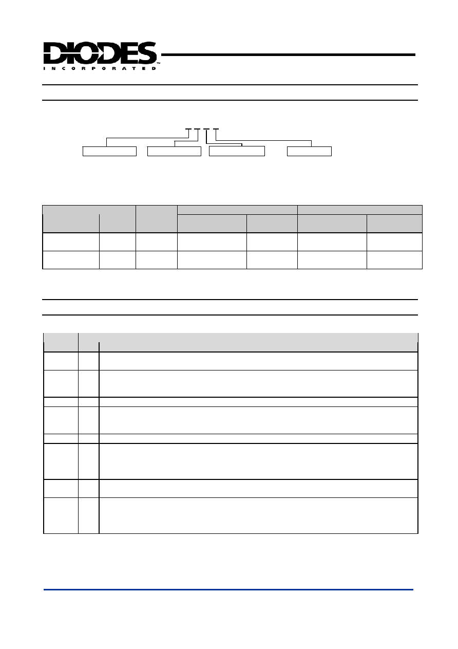
Features
General Description
Applications
Pin Assignments
AP2014/A
SYNCHRONOUS PWM DC-DC BUCK CONTROLLER
DS30883 Rev. 1 - 0
2 of 13
AP2014/A
www.diodes.com
©
Diodes Incorporated
Ordering Information
AP2014A X X X
Package
Packing
SM: SOP-8L
Blank : Tube or bulk
-7/-13 : Taping
Lead-Free
Blank : Lead-Free
G : Green
Frequency
Blank : 200KHz
A : 400KHz
Pin Descriptions
Pin
Name
Pin
No.
Description
FB 1
This pin is connected directly to the output of the switching regulator via resistor divider to
provide feedback to the Error amplifier.
Vcc 2
This pin provides biasing for the internal blocks of the IC as well as power for the low side
driver. A minimum of 1uF, high frequency capacitor must be connected from this pin to
ground to provide peak drive current capability.
LDrv
3
Output driver for the synchronous power MOSFET.
GND 4
This pin serves as the ground pin and must be connected directly to the ground plane. A
high frequency capacitor (0.1 to 1uF) must be connected from V5 and V12 pins to this pin
for noise free operation.
HDrv
5
Output driver for the high side power MOSFET.
Vc 6
This pin is connected to a voltage that must be at least 4V higher than the bus voltage of the
switcher (assuming 5V threshold MOSFET) and powers the high side output driver. A
minimum of 1uF, high frequency capacitor must be connected from this pin to ground to
provide peak drive current capability.
Comp 7
Compensation pin of the error amplifier. An external resistor and capacitor network is
typically connected from this pin to ground to provide loop compensation.
SS 8
This pin provides soft-start for the switching regulator. An internal current source charges
an external capacitor that is connected from this pin to ground which ramps up the output of
the switching regulator, preventing it from overshooting as well as limiting the input current.
The converter can be shutdown by pulling this pin below 0.5V.
7" Tape and Reel
13" Tape and Reel
Device
Package
Code
Packaging
Quantity
Part Number
Suffix
Quantity
Part Number
Suffix
AP2014SM SM SOP-8L
3000/Tape & Reel
-7
10,000/Tape &
Reel
-13
AP2014ASM SM SOP-8L
3000/Tape & Reel
-7
10,000/Tape &
Reel
-13
AP2014/A
SYNCHRONOUS PWM DC-DC BUCK CONTROLLER
DS30883 Rev. 1 - 0
3 of 13
AP2014/A
www.diodes.com
©
Diodes Incorporated
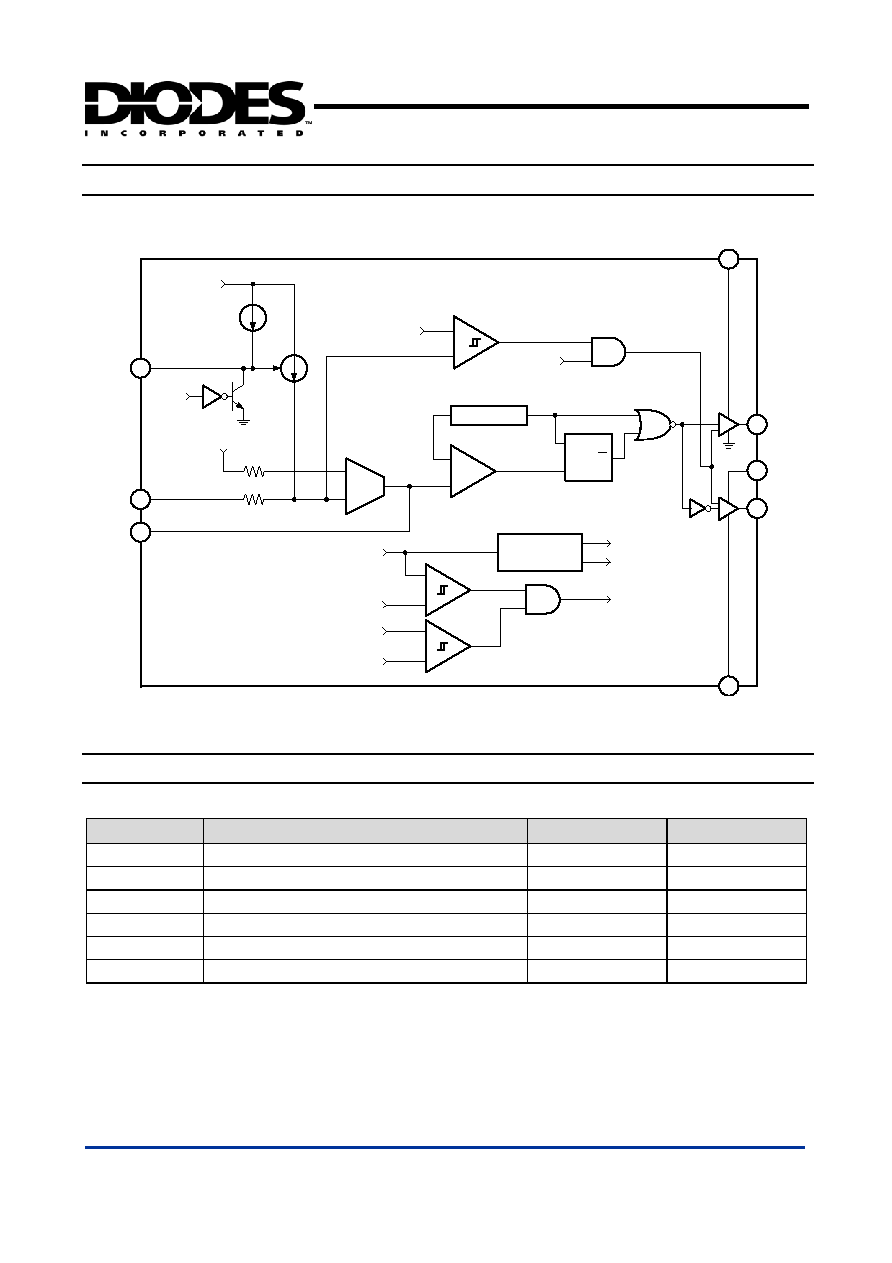
Block Diagram
SS
Fb
Comp
GND
LDrv
Vcc
HDrv
Vc
25K
25K
1.25V
POR
20uA
64uA
Max
3V
Error Amp
+
-
Oscillator
Ct
Error Comp
+
-
S
R
Q
Reset Dom
4
3
2
5
6
7
1
8
+
-
+
-
Bias
Generator
Vcc
4.0V
Vc
3.5V
0.2V
0.2V
3V
1.25V
POR
+
-
FbLo Comp
0.5V
POR
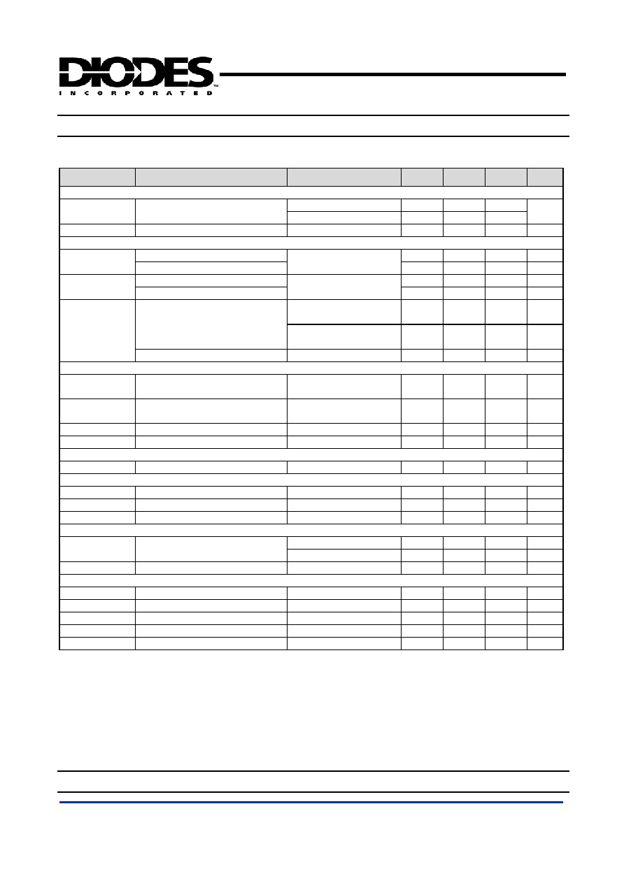
Absolute Maximum Ratings
Symbol
Parameter
Range.
Unit
V
CC
Vcc Supply Voltage
20
V
V
C
Vc Supply Voltage (not rated for inductive load)
32
V
T
ST
Storage Temperature Range
-65 to 150
o
C
T
J
Operating Junction Temperature Range
0 to 125
o
C
JC
Thermal Resistance Junction to Case
90
o
C/W
JA
Thermal Resistance Junction to Ambient
250
o
C/W
AP2014/A
SYNCHRONOUS PWM DC-DC BUCK CONTROLLER
DS30883 Rev. 1 - 0
4 of 13
AP2014/A
www.diodes.com
©
Diodes Incorporated
Electrical Characteristics
Unless otherwise specified, these specifications apply over V
CC
=5V, V
C
=12V and T
A
=0 to 70∞C. Typical values refer to T
A
=25∞C. Low
duty cycle pulse testing is used which keeps junction and case temperatures equal to the ambient temperature.
Symbol
Parameter
Conditions
Min.
Typ.
Max.
Unit
Reference Voltage
AP2014 1.225
1.25
1.275
V
FB
FB
Voltage
AP2014A 0.784
0.8
0.816
V
L
REG
FB Voltage Line Regulation
5 < Vcc < 12
-
0.2
0.35
%
UVLO
UVLO Threshold - V
CC
4.0 4.2 4.4 V
UVLO V
CC
UVLO Hysteresis - V
CC
Supply Ramping Up
- 0.25 - V
UVLO Threshold - V
C
3.1 3.3 3.5 V
UVLO V
C
UVLO Hysteresis - V
C
Supply Ramping Up
- 0.2 - V
FB Ramping Down
(AP2014)
0.4 0.6 0.8 V
UVLO Threshold - FB
FB Ramping Down
(AP2014A)
0.3 0.4 0.5 V
UVLO FB
UVLO Hysteresis - FB
-
0.1
-
V
Supply Current
Operation I
CC
V
CC
Operation Supply Current
Freq=200KHz,
C
L
=1500pF
- 7 10
mA
Operation I
C
V
C
Operation Supply Current
Freq=200KHz,
C
L
=1500pF
- 7 10
mA
I
CCQ
V
CC
Static Supply Current
SS=0V
-
3.3
6
mA
I
CQ
V
C
Static Supply Current
SS=0V
-
1
4.5
mA
Soft-Start Section
SS
IB
Charge
Current
SS=0V
10 20 30 µA
Error Amp
I
FB1
FB Voltage Input Bias Current
SS=3V,
FB=1V
- -0.1 - µA
I
FB2
FB Voltage Input Bias Current
SS=0V,
FB=1V
- -64 - µA
gm Transconductance
450 600 750
µmho
Oscillator
AP2014
170 200 230 KHz
Freq Frequency
AP2014A
340 400 460 KHz
V
RAMP
Ramp-Amplitude
Voltage
1.225
1.25
1.275 V
Output Drivers
T
r
Rise
Time
C
L
=1500pF
-
50
100
ns
T
f
Fall
Time
C
L
=1500pF
-
50
100
ns
T
DB
Dead Band Time
50
150
250
ns
T
ON
Max Duty Cycle
FB=1V, Freq=200KHz
85
90
95
%
T
OFF
Min Duty Cycle
FB=1.5V
0
0
-
%
Function Description

AP2014/A
SYNCHRONOUS PWM DC-DC BUCK CONTROLLER
DS30883 Rev. 1 - 0
5 of 13
AP2014/A
www.diodes.com
©
Diodes Incorporated
Introduction
The AP2014 is a fixed frequency, voltage mode synchronous
controller and consists of a precision reference voltage, an error
amplifier, an internal oscillator, a PWM comparator, 0.5A peak
gate driver, soft-start and shutdown circuits (see Block Diagram).
The output voltage of the synchronous converter is set and
controlled by the output of the error amplifier; this is the amplified
error signal from the sensed output voltage and the reference
voltage.
This voltage is compared to a fixed frequency linear sawtooth
ramp and generates fixed frequency pulses of variable duty-cycle,
which drives the two N-channel external MOSFETs.The timing of
the IC is provided through an internal oscillator circuit which uses
on-chip capacitor to set the oscillation frequency to 200 KHz (400
KHz for "A" version).
Soft-Start
The AP2014 has a programmable soft-start to control the output
voltage rise and limit the current surge at the start-up. To ensure
correct start-up, the soft-start sequence initiates when the V
C
and
V
CC
rise above their threshold (3.3V and 4.2V respectively) and
generates the Power On Reset (POR) signal. Soft-start function
operates by sourcing an internal current to charge an external
capacitor to about 3V. Initially, the soft-start function clamps the
E/A's output of the PWM converter. As the charging voltage of
the external capacitor ramps up, the PWM signals increase from
zero to the point the feedback loop takes control.
The outputs are protected against the short circuit. The AP2014
protects the circuit for shorted output by sensing the output
voltage (through the external resistor divider). The AP2014 shuts
down the PWM signals, when the output voltage drops below
0.6V (0.4V for AP2014A).
The AP2014 also protects the output from over-voltaging when
the control FET is shorted. This is done by turning on the sync
FET with the maximum duty cycle.
Under-Voltage Lockout
The under-voltage lockout circuit assures that the MOSFET
driver outputs remain in the off state whenever the supply voltage
drops below set parameters. Lockout occurs if V
C
and V
CC
fall
below 3.3V and 4.2V respectively. Normal operation resumes
once V
C
and V
CC
rise above the set values.
IC Quiescent Power Dissipation
Power dissipation for PWM DC-DC controller IC is a function of
applied voltage, gate driver loads and switching frequency. The
IC's maximum power dissipation occurs when the IC operating
with single 12V supply voltage (Vcc=12V and Vc
24V) at 400KHz
switching frequency and maximum gate loads. Page 8 show
voltage vs. current, when the gate drivers loaded with 1500pF
capacitors. The IC's power dissipation results to an excessive
temperature rise. This should be considered when using
AP2014A for such application.
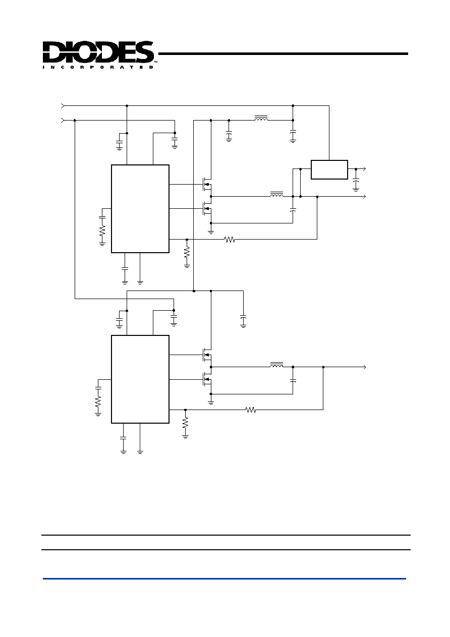
Typical Application Circuit

AP2014/A
SYNCHRONOUS PWM DC-DC BUCK CONTROLLER
DS30883 Rev. 1 - 0
6 of 13
AP2014/A
www.diodes.com
©
Diodes Incorporated
(1)
C6
10nF
Q2
AF9410N
C17
0.1u
VIN=5V
C3
1u
C12
470u
Vc=12V
C8
470u
Vout +1.5V/7.0A
Q1
AF9410N
L1
5.6u/9.0
R6
22k
AP2014
C13
470u
C20
100p
C5
0.47u
R3
8.2
C4
0.1u
R2
3.3K
C11
0.1u
R1
820
U1
1
2
3
4
5
6
7
8
FB
Vcc
LDrv
GND HDrv
Vc
Comp
SS
(2)
Vout +1.5V/7.0A
C5
0.47u
R3
8.2
C13
470u
C1
0.1uF
C8
470u
D1
1N4148
R2
3.3K
C11
0.1u
U1
AP2014
1
2
3
4
5
6
7
8
FB
Vcc
LDrv
GND HDrv
Vc
Comp
SS
C12
470u
R1
820
Q1
AF9410N
R6
6.8k
VIN=12V
C20
100p
Option
C4
0.1u
C6
10nF
Q2
AF9410N
C17
0.1u
1N4148
D2
C3
100u
L1
5.6u/9A
Single Supply 12V Input
Typical Application Circuit (Continued)

AP2014/A
SYNCHRONOUS PWM DC-DC BUCK CONTROLLER
DS30883 Rev. 1 - 0
7 of 13
AP2014/A
www.diodes.com
©
Diodes Incorporated
(3)
Vout +5V/5.0A
C5
0.47u
R3
8.2
C13
470u
C1
0.1uF
C8
470u
D1
1N4148
R2
3K
C11
0.1u
U1
AP2014
1
2
3
4
5
6
7
8
FB
Vcc
LDrv
GND HDrv
Vc
Comp
SS
R1
10K
Q1
AF4910N-1
R6
39k
VIN=12V
C20
100p
C4
0.1u
C6
10nF
Q2
AF4910N-2
C17
0.1u
1N4148
D2
C3
100u
L1
10uH/6A
Single Supply 12V Input
(4)
Vout +5V/4.0A
C5
0.47u
R3
8.2
C13
470u
C1
0.1uF
C8
470u
D1
1N4148
R2
3.3K
C11
0.1u
U1
AP2014
1
2
3
4
5
6
7
8
FB
Vcc
LDrv
GND HDrv
Vc
Comp
SS
R1
10K
Q1-1
AF4928N-1
R6
47k
VIN=24V
C20
100p
C4
0.1u
C6
10nF
Q1-2
AF4928N-2
C17
0.1u
1N4148
D2
C3
100u
L1
10uH/6A
1.2K
RZD
R3
8.2
ZD
6.2V
I
ZD
(
15mA)=(VIN-V
D2
-V
ZD
)/RZD
Single Supply 24V Input
Typical Application Circuit (Continued)
AP2014/A
SYNCHRONOUS PWM DC-DC BUCK CONTROLLER
DS30883 Rev. 1 - 0
8 of 13
AP2014/A
www.diodes.com
©
Diodes Incorporated
(5) Dual Supply, 5V Bus and 12V Bias Input
SS
Fb
Comp
GND
LDrv
Vcc
HDrv
Vc
+
+
+
AP2014
C7
0.1uF
C8
10nF
R1
3.3K
R2
1K
R3
1K
Q1
Q2
AF9410
L2
10uH
C3
100uF
L1
1uH
C4
47uF
1.8V/1A
2.5V/2A
C6
C1
0.1uF
AP1187
+
5V
12V
SS
Fb
Comp
GND
LDrv
Vcc
HDrv
Vc
+
+
AP2014
C13
0.1uF
C14
10nF
R4
3.3K
R5
1K
R6
1.65K
Q3
AF9410
Q4
AF9410
L3
C11
3.3V/1.8A
C12
220uF
C9
0.1uF
C1
1uF
C5
47uF
C10
1uF
10uH
AF9410
220uF
Dual Supply, 5V Bus and 12V Bias Input
Typical Performance Characteristics

AP2014/A
SYNCHRONOUS PWM DC-DC BUCK CONTROLLER
DS30883 Rev. 1 - 0
9 of 13
AP2014/A
www.diodes.com
©
Diodes Incorporated
Load Regulation
0.0%
0.2%
0.4%
0.6%
0.8%
1.0%
1.2%
1.4%
1.6%
1.8%
2.0%
0.0 0.5 1.0 3.0 5.0 8.0 10.0 12.0 15.0
Iout(A)
Lo
ad
R
e
g
u
l
a
t
i
o
n
(
%
)
Efficiency vs. Iout
0%
10%
20%
30%
40%
50%
60%
70%
80%
90%
100%
0.0 0.5 1.0 3.0 5.0 8.0 10.0 12.0 15.0
Iout(A)
Efficiency (%)
Line Regulation
1.240
1.245
1.250
1.255
1.260
4.5
5.0
7.0
9.0
11.0 12.0 15.0
Vin(V)
F
e
ed
ba
c
k
V
o
l
t
a
g
e
(
V
)
Line Regulation
2.500
2.505
2.510
2.515
2.520
2.525
2.530
4.5 5.0 7.0 9.0 11.0 12.0 15.0
Vin(V)
O
u
t
put
V
o
l
t
age (
V
)
Frequency v.s. Vin
175.0
180.0
185.0
190.0
195.0
200.0
205.0
210.0
4.5 5.0
7.0
9.0 11.0 12.0 15.0
Vin(V)
F
r
eq
ue
n
c
y
(
K
H
z
)
Frequency v.s. Temperature
150.0
160.0
170.0
180.0
190.0
200.0
210.0
220.0
230.0
240.0
-40 -20
0
25
50
75
100 125
Temperature (
o
C)
F
r
eq
ue
nc
y
(
K
Hz
)
Typical Performance Characteristics (Continued)

AP2014/A
SYNCHRONOUS PWM DC-DC BUCK CONTROLLER
DS30883 Rev. 1 - 0
10 of 13
AP2014/A
www.diodes.com
©
Diodes Incorporated
Icc and Iccq vs. Vin
3.00
5.00
7.00
9.00
11.00
13.00
15.00
4.5
5
7
9
11
12
15
Vin(V)
Icc and Iccq (mA)
Icc(mA)
Iccq(mA)
Ic and Icq vs. Vin
2.00
4.00
6.00
8.00
10.00
12.00
14.00
16.00
4.5
5
7
9
11
12
15
Vin(V)
Ic and Icq (mA)
Ic(mA)
Icq(mA)
Icc and Ic vs. Temperature
6.0
6.5
7.0
7.5
8.0
8.5
9.0
9.5
10.0
-40
-20
0
25
50
75
100 125
Temperature (
o
C)
Icc and Ic (mA)
Icc(mA)
Ic(mA)
Vfb vs. Temperature
1.20
1.22
1.24
1.26
1.28
1.30
-40 -20
0
25
50
75
100 125
Temperature (
o
C)
F
eedback Voltage (V)
AP2014A Ic and Icc vs Vc
3.0
5.0
7.0
9.0
11.0
13.0
15.0
17.0
19.0
21.0
6
8
10 12 14 16 18 20 22 24
Vc(V)
Ic(mA)
Icc(mA)
AP2014 Ic and Icc vs Vc
2.0
4.0
6.0
8.0
10.0
12.0
14.0
16.0
18.0
20.0
6
8
10 12 14 16 18 20 22 24
Vc(V)
Ic(mA)
Icc(mA)
Typical Performance Characteristics (Continued)
AP2014/A
SYNCHRONOUS PWM DC-DC BUCK CONTROLLER
DS30883 Rev. 1 - 0
11 of 13
AP2014/A
www.diodes.com
©
Diodes Incorporated
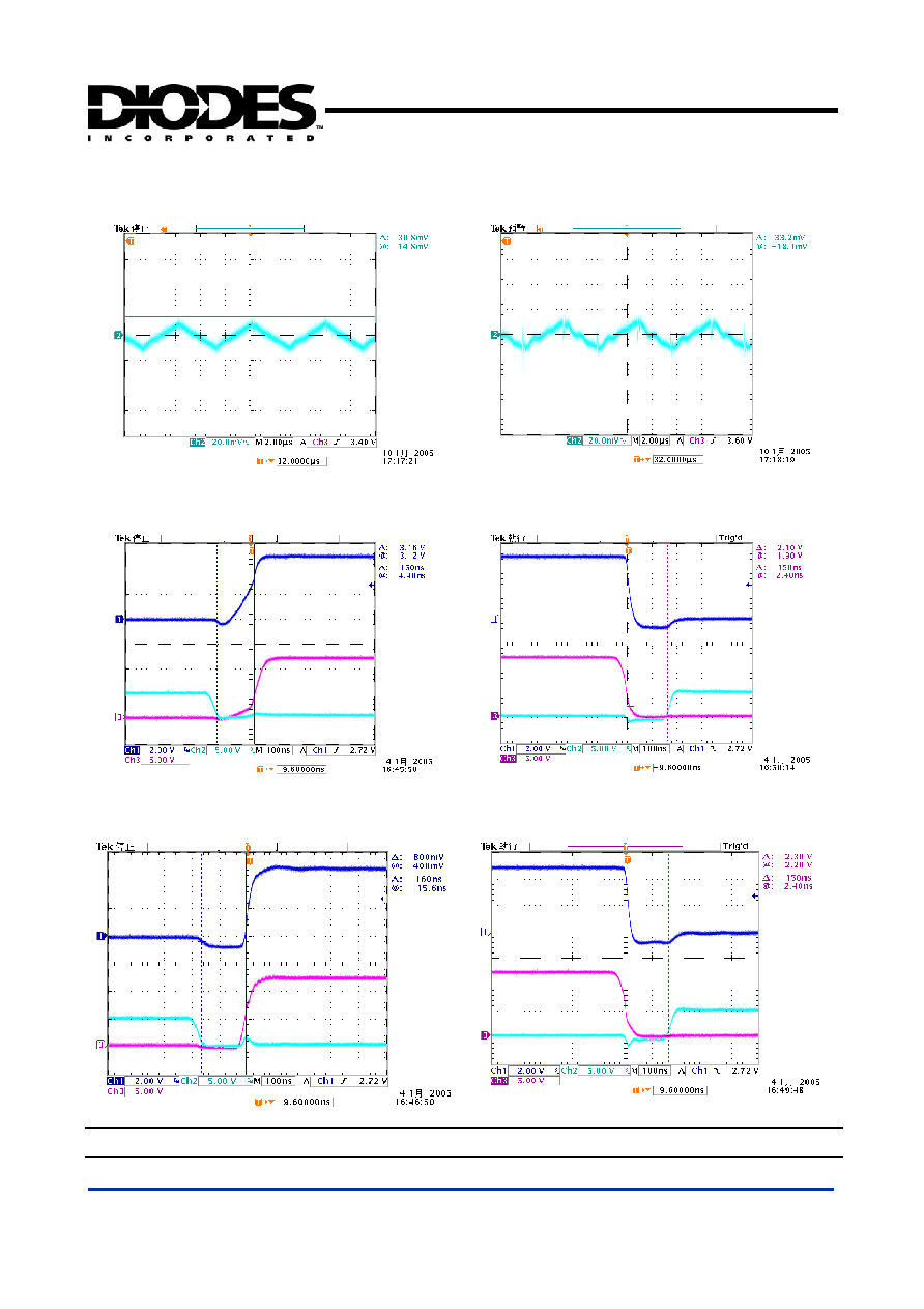
Vout Ripple
Vcc=5V; Vc=12V; Vout=2.5V
Iout=0.5A, Vripple=30.8mV
Vout Ripple
Vcc=5V; Vc=12V; Vout=2.5V
Iout=5A, Vripple=33.2mV
Dead time v.s. Iout
Vcc=5V, Vc=12V, Vout=2.5V, Iout=0.5A, Temp=28
o
C
Dead time = 150ns
Dead time = 150ns
Dead time v.s. Iout
Vcc=5V, Vc=12V, Vout=2.5V, Iout=5A , Temp=28
o
C
Dead time = 160ns
Dead time = 150ns
Marking Information
Highside GATE
Lowside GATE
Phase
Lowside GATE
Highside GATE
Phase
AP2014/A
SYNCHRONOUS PWM DC-DC BUCK CONTROLLER
DS30883 Rev. 1 - 0
12 of 13
AP2014/A
www.diodes.com
©
Diodes Incorporated
(1) SOP-8L
AP2014(A)
(Top view)
Y WW
Part Number
Logo
WW: Nth week
Y: Year
X
Blank : Lead Free
G : Green
Marking Code Table
Device
Package
Marking Code
Date Code
AP2014 SOP-8L
AP2014
YWW
AP2014A SOP-8L
AP2014A
YWW
Date Code Key
Year 2006 2007
2008 2009 2010
2011 2012
2013 2014
2015 2016 2017
Code
T U V W X Y Z A B C D E
Package Information
(All Dimensions in mm)
Package Type: SOP-8L

AP2014/A
SYNCHRONOUS PWM DC-DC BUCK CONTROLLER
DS30883 Rev. 1 - 0
13 of 13
AP2014/A
www.diodes.com
©
Diodes Incorporated
3.85/3.95
Typ 3.90
3.80/3.90
Typ 3.85
7∞
45
∞
0.60/0.70
Typ 0.65
0.15/0.25
Typ 0.20
0.60/0.80
Typ 0.70
1.27
4.85/4.95
Typ 4.90
1.40/1.50
Typ 1.45
0.30/0.50
Typ 0.40
5.90/6.10
Typ 6.00
5
4
1
8
0.08/0.25
Typ 0.15
R
0.1
(All s
ide)
9∞
4∞
3∞
±
0.35
RECOMMENDED LAND PATTERN
8X 2.2
5.2
6X 1.27
8X .06