
DS13005 Rev. 8 - 2
1 of 3
B320/A/B-B360/A/B
www.diodes.com
B320/A/B - B360/A/B
3.0A SURFACE MOUNT SCHOTTKY BARRIER RECTIFIER
Features
Maximum Ratings and Electrical Characteristics
@ T
A
= 25∞C unless otherwise specified
∑
Guard Ring Die Construction for Transient
Protection
∑
Ideally Suited for Automatic Assembly
∑
Low Power Loss, High Efficiency
∑
Surge Overload Rating to 100A Peak
∑
For Use in Low Voltage, High Frequency
Inverters, Free Wheeling, and Polarity
Protection Application
Mechanical Data
∑
Case: Molded Plastic
∑
Plastic Material - UL Flammability
Classification 94V-0
∑
Moisture sensitivity: Level 1 per J-STD-020A
∑
Terminals: Solder Plated Terminal -
Solderable per MIL-STD-202, Method 208
∑
Polarity: Cathode Band
∑
Approx. Weight: SMA 0.064 grams
SMB 0.093 grams
SMC 0.21 grams
∑
Marking: Type Number (See Page 3)
"A" Suffix Designates SMA Package
"B" Suffix Designates SMB Package
No Suffix Designates SMC Package
*
: Note: Device may have a semicircular indentation/
notch on one side of the device (as shown).
Single phase, half wave, 60Hz, resistive or inductive load.
For capacitive load, derate current by 20%.
SMA
SMB
SMC
Dim
Min
Max
Min
Max
Min
Max
A
2.29 2.92 3.30 3.94 5.59 6.22
B
4.00 4.60 4.06 4.57 6.60 7.11
C
1.27 1.63 1.96 2.21 2.75 3.18
D
0.15 0.31 0.15 0.31 0.15 0.31
E
4.80 5.59 5.00 5.59 7.75 8.13
G
0.10 0.20 0.10 0.20 0.10 0.20
H
0.76 1.52 0.76 1.52 0.76 1.52
J
2.01 2.62 2.00 2.62 2.00 2.62
All Dimensions in mm
A
B
C
D
G
*
H
E
J
Characteristic
Symbol
B320/A/B B330/A/B B340/A/B B350/A/B B360/A/B
Unit
Peak Repetitive Reverse Voltage
Working Peak Reverse Voltage
DC Blocking Voltage
V
RRM
V
RWM
V
R
20
30
40
50
60
V
RMS Reverse Voltage
V
R(RMS)
14
21
28
35
42
V
Average Rectified Output Current
@ T
T
= 100∞C
I
O
3.0
A
Non-Repetitive Peak Forward Surge Current, 8.3ms
single half sine-wave superimposed on rated load
(JEDEC Method)
I
FSM
100
A
Forward Voltage (Note 3)
@ I
F
= 3.0A
V
FM
0.50
0.70
V
Peak Reverse Current
@T
A
= 25∞C
at Rated DC Blocking Voltage (Note 3)
@T
A
= 100∞C
I
RM
0.5
20
mA
Typical Capacitance (Note 2)
C
T
250
pF
Typical Thermal Resistance, Junction to Terminal (Note 1)
R
qJT
10
∞C/W
Typical Thermal Resistance, Junction to Ambient
R
qJA
50
∞C/W
Operating Temperature Range
T
j
-55 to +125
∞C
Storage Temperature Range
T
STG
-55 to +150
∞C
Notes:
1. Thermal Resistance: Junction to terminal, unit mounted on PC board with 5.0 mm
2
0.013 mm thick) copper pad as heat sink.
2. Measured at 1.0 MHz and applied reverse voltage of 4.0V DC.
3. Short duration test pulse used to minimize self-heating effect.
SPICE MODELS: B320 B330 B340 B350 B360
DS13005 Rev. 8 - 2
2 of 3
B320/A/B-B360/A/B
www.diodes.com
0.1
1.0
10
0.1
0.3
0.4
0.2
0.5
0.6
0.7
0.8
I
,
INST
ANT
A
NEOUS
FWD
CURRENT
(A)
F
V , INSTANTANEOUS FORWARD VOLTAGE (V)
F
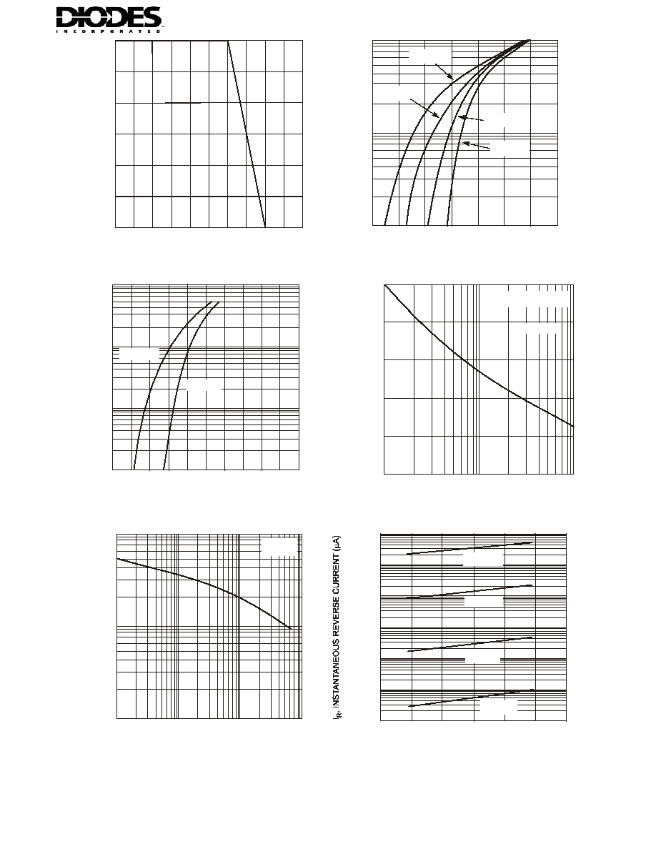
Fig. 2 Typical Forward Characteristics - B320/A/B thru B340/A/B
T = +25
∞C
A
T = +75
∞C
A
T = +125
∞C
A
T = -25
∞C
A
0.01
0.1
1.0
10
0
0.2
0.4
0.6
0.8
1.0
I
,
INST
ANT
ANEOUS
FOR
W
ARD
CURRENT
(A)
F
V , INSTANTANEOUS FORWARD VOLTAGE (V)
F
Fig. 3 Typ. Forward Characteristics - B350/A/B thru B360/A/B
T = +125∫C
A
T = +25∫C
A
0
20
40
60
80
100
1
10
100
I
,
PEAK
FOR
W
A
RD
SURGE
CURRENT
(A)
FSM
NUMBER OF CYCLES AT 60 Hz
Fig. 4 Max Non-Repetitive Peak Fwd Surge Current
Single Half-Sine-Wave
(JEDEC Method)
T = 100∞C
T
0
0.5
1.0
25
50
75
100
125
150
I
A
VERAGE
FOR
W
A
RD
CURRENT
(A)
(A
V),
T , TERMINAL TEMPERATURE (
∞C)
T
Fig. 1 Forward Current Derating Curve
1.5
2.0
2.5
3.0
100
10
1
0.1
0.01
1000
10,000
0
20
40
60
V , INSTANTANEOUS REVERSE VOLTAGE (V)
R
Fig. 6 Typical Reverse Characteristics, B320/A/B thru B340/A/B
10
30
50
T = +25
∞C
A
T = +125
∞C
A
T = -25
∞C
A
T = +75
∞C
A
10
100
1000
0.1
1
10
100
C
,
T
O
T
A
L
C
AP
ACIT
ANCE
(pF)
T
V , REVERSE VOLTAGE (V)
R
Fig. 5 Typical Capacitance
f = 1 MHz
T = 25∞C
J

B
= Manufacturers' code marking
YWW = Date code marking
Y = Last digit of year ex: 2 for 2002
WW = Week code 01 to 52
XXX = Product type marking code, ex: B320 (SMC package)
BXXXX = Product type marking code, ex: B320A (SMA package)
YWW
BXXX(X)
DS13005 Rev. 8 - 2
3 of 3
B320/A/B-B360/A/B
www.diodes.com
100
10
1
0.1
1000
10,000
0
20
40
60
70
V , INSTANTANEOUS REVERSE VOLTAGE (V)
R
Fig. 7 Typical Reverse Characteristics, B350/A/B thru B360/A/B
10
30
50
T = +25
∞C
A
T = +125
∞C
A
T = +70
∞C
A
Ordering Information
(Note 3)
Device*
Packaging
Shipping
B3XXA-13
SMA
5000/Tape & Reel
B3XXB-13
SMB
3000/Tape & Reel
B3XX-13
SMC
3000/Tape & Reel
Notes:
3. For Packaging Details, go to our website at http://www.diodes.com/datasheets/ap02007.pdf.
* xx = Device type, e.g. B320A-13 (SMA package); B320B-13 (SMB package); B320-13 (SMC Package).
Note: Device has a cathode band (as shown above) and may also have a cathode notch (as shown on Page 1).