 | –≠–ª–µ–∫—Ç—Ä–æ–Ω–Ω—ã–π –∫–æ–º–ø–æ–Ω–µ–Ω—Ç: BAS85/T1 | –°–∫–∞—á–∞—Ç—å:  PDF PDF  ZIP ZIP |

DATA SHEET
Product specification
Supersedes data of 1996 Mar 20
1996 Oct 01
DISCRETE SEMICONDUCTORS
BAS85
Schottky barrier diode
lfpage
M3D121

1996 Oct 01
2
Philips Semiconductors
Product specification
Schottky barrier diode
BAS85
FEATURES
∑
Low forward voltage
∑
High breakdown voltage
∑
Guard ring protected
∑
Hermetically-sealed small SMD
package.
APPLICATIONS
∑
Ultra high-speed switching
∑
Voltage clamping
∑
Protection circuits
∑
Blocking diodes.
DESCRIPTION
Planar Schottky barrier diode with an
integrated protection ring against
static discharges.
This surface mounted diode is
encapsulated in a hermetically sealed
SOD80C glass SMD package with
tin-plated metal discs at each end. It
is suitable for "automatic placement"
and as such it can withstand
immersion soldering.
Fig.1 Simplified outline (SOD80C), pin configuration and symbol.
handbook, halfpage
MAM190
k
a
Cathode indicated by a grey band.
LIMITING VALUES
In accordance with the Absolute Maximum Rating System (IEC 134).
Note
1. Refer to SOD80 standard mounting conditions.
SYMBOL
PARAMETER
CONDITIONS
MIN.
MAX.
UNIT
V
R
continuous reverse voltage
-
30
V
I
F
continuous forward current
-
200
mA
I
F(AV)
average forward current
V
RWM
= 25 V; a = 1.57;
= 0.5;
note 1; Fig.2
-
200
mA
I
FRM
repetitive peak forward current
t
p
1 s;
0.5
-
300
mA
I
FSM
non-repetitive peak forward current
t
p
= 10 ms
-
5
A
T
stg
storage temperature
-
65
+150
∞
C
T
j
junction temperature
-
125
∞
C
T
amb
operating ambient temperature
-
65
+125
∞
C

1996 Oct 01
3
Philips Semiconductors
Product specification
Schottky barrier diode
BAS85
ELECTRICAL CHARACTERISTICS
T
amb
= 25
∞
C unless otherwise specified.
Note
1. Pulsed test: t
p
= 300
µ
s;
= 0.02.
THERMAL CHARACTERISTICS
Note
1. Refer to SOD80 standard mounting conditions.
SYMBOL
PARAMETER
CONDITIONS
MAX.
UNIT
V
F
forward voltage
see Fig.3
I
F
= 0.1 mA
240
mV
I
F
= 1 mA
320
mV
I
F
= 10 mA
400
mV
I
F
= 30 mA
500
mV
I
F
= 100 mA
800
mV
I
R
reverse current
V
R
= 25 V; note 1; see Fig.4
2.3
µ
A
C
d
diode capacitance
f = 1 MHz; V
R
= 1 V; see Fig.5
10
pF
SYMBOL
PARAMETER
CONDITIONS
VALUE
UNIT
R
th j-a
thermal resistance from junction to ambient
note 1
320
K/W
1996 Oct 01
4
Philips Semiconductors
Product specification
Schottky barrier diode
BAS85
GRAPHICAL DATA
Fig.2 Derating curve.
handbook, halfpage
0
50
100
150
200
250
0
50
100
150
IF(AV)
(mA)
T ( C)
amb
o
MRA540
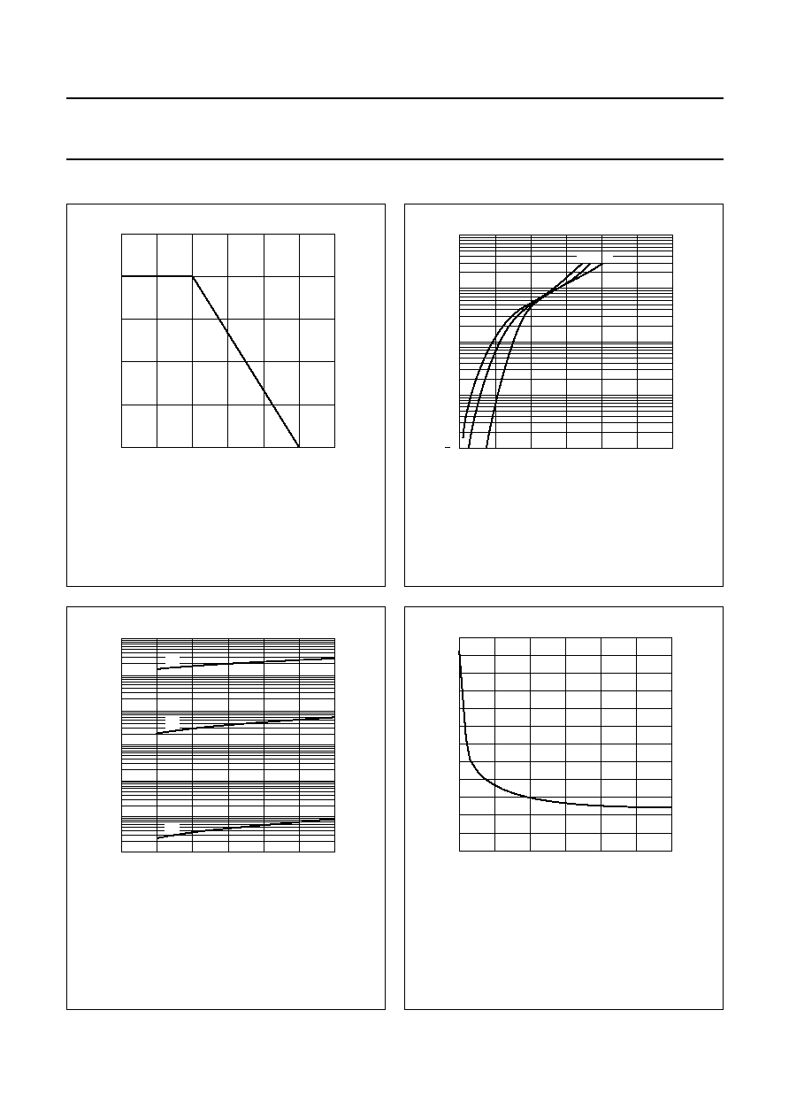
Fig.3
Forward current as a function of forward
voltage; typical values.
handbook, halfpage
10
IF
VF (V)
3
10
(mA)
2
10
1
10
1
1.2
0.8
0.4
0
MSA892
(3)
(2)
(1)
(3)
(2)
(1)
(1) T
amb
= 125
∞
C.
(2) T
amb
= 85
∞
C.
(3) T
amb
= 25
∞
C.
Fig.4
Reverse current as a function of reverse
voltage; typical values.
handbook, halfpage
10
(nA)
I
R
5
10
4
10
3
10
2
10
10
1
-
1
30
20
V
R
(V)
10
0
MGC682
(1)
(2)
(3)
(1) T
amb
= 85
∞
C.
(2) T
amb
= 25
∞
C.
(3) T
amb
=
-
40
∞
C.
Fig.5
Diode capacitance as a function of reverse
voltage; typical values.
f = 1 MHz.
handbook, halfpage
0
10
20
V
R
(V)
30
12
(pF)
C
d
0
4
8
MGC681

1996 Oct 01
5
Philips Semiconductors
Product specification
Schottky barrier diode
BAS85
PACKAGE OUTLINE
DEFINITIONS
LIFE SUPPORT APPLICATIONS
These products are not designed for use in life support appliances, devices, or systems where malfunction of these
products can reasonably be expected to result in personal injury. Philips customers using or selling these products for
use in such applications do so at their own risk and agree to fully indemnify Philips for any damages resulting from such
improper use or sale.
Data sheet status
Objective specification
This data sheet contains target or goal specifications for product development.
Preliminary specification
This data sheet contains preliminary data; supplementary data may be published later.
Product specification
This data sheet contains final product specifications.
Limiting values
Limiting values given are in accordance with the Absolute Maximum Rating System (IEC 134). Stress above one or
more of the limiting values may cause permanent damage to the device. These are stress ratings only and operation
of the device at these or at any other conditions above those given in the Characteristics sections of the specification
is not implied. Exposure to limiting values for extended periods may affect device reliability.
Application information
Where application information is given, it is advisory and does not form part of the specification.
Dimensions in mm.
Cathode indicated by a grey band.
Fig.6 SOD80C.
handbook, full pagewidth
MBA390 - 2
1.60
1.45
3.7
3.3
0.3
0.3
O