DS30145 Rev. C-2
1 of 3
BAV99DW
BAV99DW
QUAD SURFACE MOUNT SWITCHING DIODE ARRAY
∑
Case: SOT-363, Molded Plastic
∑
Terminals: Solderable per MIL-STD-202,
Method 208
∑
Polarity: See Diagram
∑
Marking: KJG
∑
Weight: 0.006 grams (approx.)
∑
Case Material - UL Flammability Rating
Classification 94V-0
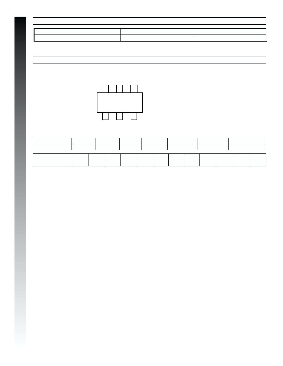
Mechanical Data
A
M
J
L
F
D
B C
H
K
AC
1
AC
2
C
2
A
1
A
2
C
1
Features
SOT-363
Dim
Min
Max
A
0.10
0.30
B
1.15
1.35
C
2.00
2.20
D
0.65 Nominal
E
0.30
0.40
G
1.80
2.20
H
1.80
2.20
J
æ
0.10
K
0.90
1.00
L
0.25
0.40
M
0.10
0.25
All Dimensions in mm
∑
Fast Switching Speed
∑
Ultra-Small Surface Mount Package
∑
For General Purpose Switching Applications
∑
High Conductance
∑
Two "BAV99" Circuits In One Package
Characteristic
Symbol
BAV99DW
Unit
Non-Repetitive Peak Reverse Voltage
V
RM
100
V
Peak Repetitive Reverse Voltage
Working Peak Reverse Voltage
DC Blocking Voltage
V
RRM
V
RWM
V
R
75
V
RMS Reverse Voltage
V
R(RMS)
53
V
Forward Continuous Current
I
FM
215
mA
Non-Repetitive Peak Forward Surge Current @ t = 1.0
ms
@ t = 1.0ms
@ t = 1.0s
I
FSM
2.0
1.0
0.5
A
Power Dissipation (Note 1)
P
d
200
mW
Thermal Resistance Junction to Ambient Air (Note 1)
R
qJA
625
∞C/W
Power Dissipation (Note 2)
P
d
300
mW
Thermal Resistance Junction to Ambient Air (Note 2)
R
qJA
417
∞C/W
Operating and Storage Temperature Range
T
j
, T
STG
-65 to +150
∞C
Maximum Ratings
@ T
A
= 25
∞C unless otherwise specified
Notes:
1. Device mounted on FR-4 PCB, 1 inch x 0.85 inch x 0.062 inch; pad layout as shown on Diodes Inc. suggested pad layout
document AP02001, which can be found on our website at http://www.diodes.com/datasheets/ap02001.pdf.
2. Device mounted on Alumina PCB, 0.4 inch x 0.3 inch x 0.024 inch; pad layout as shown on Diodes Inc. suggested pad layout
document AP02001, which can be found on our website at http://www.diodes.com/datasheets/ap02001.pdf.
Characteristic
Symbol
Min
Max
Unit
Test Condition
Maximum Forward Voltage
V
FM
æ
0.715
0.855
1.0
1.25
V
I
F
= 1.0mA
I
F
= 10mA
I
F
= 50mA
I
F
= 150mA
Maximum Peak Reverse Current
I
RM
æ
2.5
50
30
25
mA
mA
mA
nA
V
R
= 75V
V
R
= 75V, T
j
= 150
∞C
V
R
= 25V, T
j
= 150
∞C
V
R
= 20V
Junction Capacitance
C
j
æ
2.0
pF
V
R
= 0, f = 1.0MHz
Reverse Recovery Time
t
rr
æ
4.0
ns
I
F
= I
R
= 10mA,
I
rr
= 0.1 x I
R
, R
L
= 100
W
Electrical Characteristics
@ T
A
= 25
∞C unless otherwise specified
NEW
PRODUCT

DS30145 Rev. C-2
3 of 3
BAV99DW
1
10
100
1000
10,000
0
100
200
I
,
LEAKAGE
CURRENT
(nA)
R
T , JUNCTION TEMPERATURE (∞C)
Fig. 2 Leakage Current vs Junction Temperature
j
V = 20V
R
10
1.0
100
1000
0.1
0.01
0
1
2
I
,
INST
ANT
ANE
O
US
F
O
R
W
ARD
CURRENT
(mA)
F
V , INSTANTANEOUS FORWARD VOLTAGE (V)
Fig. 1 Forward Characteristics
F
C
,
CAP
ACIT
ANCE
(pF)
j
f = 1MHz
V REVERSE VOLTAGE (V)
Fig. 3 Typical Junction Capacitance vs Reverse Voltage
R,
0.1
100
10
1.0
0
0.2
0.4
0.6
0.8
1.0
1.2
1.4
1.6
1.8