DS30068 Rev. 2 - 2
1 of 2
LLSD103A - 103C
LLSD103A - 103C
SURFACE MOUNT SCHOTTKY BARRIER DIODE
Features
∑
Low Forward Voltage Drop
∑
Guard Ring Construction for Transient
Protection
∑
Fast Reverse Recovery Time
∑
Low Reverse Capacitance
∑
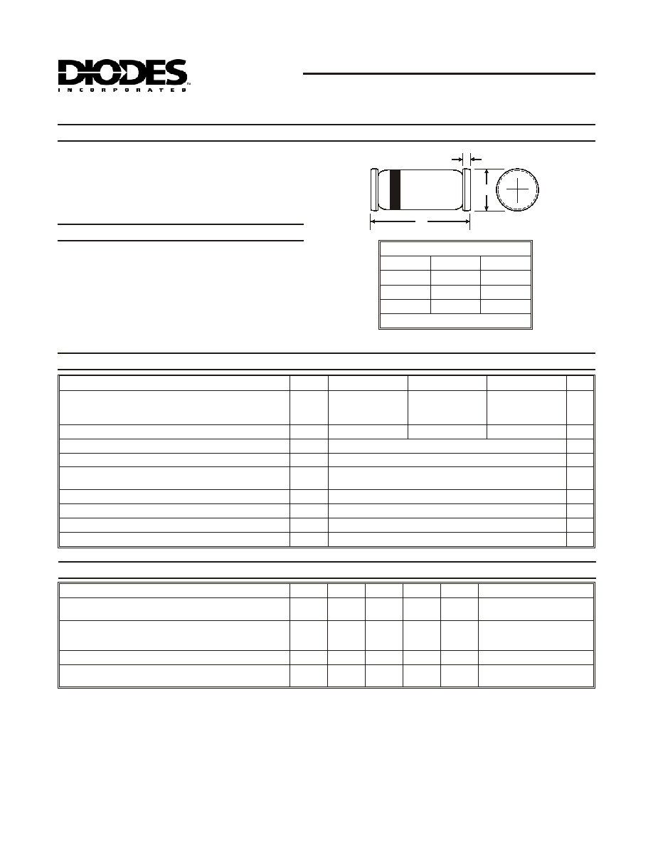
Case: MiniMELF, Glass
∑
Terminals: Solderable per MIL-STD-202,
Method 208
∑
Marking: Cathode Band Only
∑
Polarity: Cathode Band
∑
Weight: 0.05 grams (approx.)
Mechanical Data
MiniMELF
Dim
Min
Max
A
3.30
3.70
B
1.30
1.60
C
0.28
0.50
All Dimensions in mm
A
C
B
Maximum Ratings
@ T
A
= 25
∞C unless otherwise specified
Note:
1. Part mounted on FR-4 board with recommended pad layout, which can be found on our website
at http://www.diodes.com/datasheets/ap02001.pdf.
2. Short duration test pulse used to minimize self-heating effect.
Electrical Characteristics
@ T
A
= 25
∞C unless otherwise specified
Characteristic
Symbol
LLSD103A
LLSD103B
LLSD103C
Unit
Peak Repetitive Reverse Voltage
Working Peak Reverse Voltage
DC Blocking Voltage
V
RRM
V
RWM
V
R
40
30
20
V
RMS Reverse Voltage
V
R(RMS)
28
21
14
V
Forward Continuous Current (Note 1)
I
FM
350
mA
Repetitive Peak Forward Current
@ t
£ 1.0s
I
FRM
1.0
A
Non-Repetitive Peak Forward Surge Current
@ t
£ 1.0s
@ t = 10ms
I
FSM
1.5
7.5
A
Power Dissipation (Note 1)
P
d
400
mW
Thermal Resistance, Junction to Ambient Air (Note 1)
R
qJA
250
∞C/W
Operating Temperature Range
T
j
-55 to +125
∞C
Storage Temperature Range
T
STG
-55 to +150
∞C
Characteristic
Symbol
Min
Typ
Max
Unit
Test Condition
Forward Voltage Drop (Note 2)
V
F
æ
æ
0.37
0.60
V
I
F
= 20mA
I
F
= 200mA
Peak Reverse Current (Note 2)
LLSD103A
LLSD103B
LLSD103C
I
R
æ
æ
5.0
mA
V
R
= 30V
V
R
= 20V
V
R
= 10V
Total Capacitance
C
T
æ
50
æ
pF
V
R
= 0V, f = 1.0MHz
Reverse Recovery Time
t
rr
æ
æ
10
ns
I
F
= I
R
= 50mA to 200mA,
I
rr
= 0.1 x I
R
, R
L
= 100
W

DS30068 Rev. 2 - 2
2 of 2
LLSD103A - 103C
1.0
10
100
1000
0.10
0.01
0
0.5
1.0
I,
F
O
R
W
ARD
C
URRENT
(mA)
F
V , FORWARD VOLTAGE (V)
F
Fig. 1 Typical Forward Characteristics
0
1
2
3
4
5
0
0.5
1.0
1.5
I
,
FOR
W
ARD
C
URRENT
(A)
F
V , FORWARD VOLTAGE (V)
F
Fig. 2 Typical High Current Fwd Characteristics
t = 300
ms
p
duty cycle = 2%
0
10
20
30
40
50
0
100
200
V
,
REVERSE
V
OL
T
A
GE
(V)
R
T , AMBIENT TEMPERATURE (
∞C)
A
Fig. 3 Blocking Voltage Derating Curves
100mA
200mA
I = 400mA
F
Notes:
3. For Packaging Details, go to our website at http://www.diodes.com/datasheets/ap02007.pdf.
Device
Packaging
Shipping
LLSD103A-7
LLSD103A-13
LLSD103B-7
LLSD103B-13
LLSD103C-7
LLSD103C-13
MiniMELF
3000/Tape & Reel
10000/Tape & Reel
3000/Tape & Reel
10000/Tape & Reel
3000/Tape & Reel
10000/Tape & Reel
Ordering Information
(Note 3)