DS30356 Rev. 2 - 1
1 of 3
SBM1040CT
www.diodes.com
SBM1040CT
10A SURFACE MOUNT DUAL SCHOTTKY BARRIER RECTIFIER
POWERMITE“3
Features
Single phase, half wave, 60Hz, resistive or inductive load.
For capacitive load, derate current by 20%.
∑
Case: POWERMITE
‚3 Molded Plastic
∑
Moisture sensitivity: Level 1 per J-STD-020A
∑
Terminals: Solderable per MIL-STD-202,
Method 208
∑
Polarity: See Diagram
∑
Marking: See Sheet 2
∑
Weight: 0.072 grams (approx.)
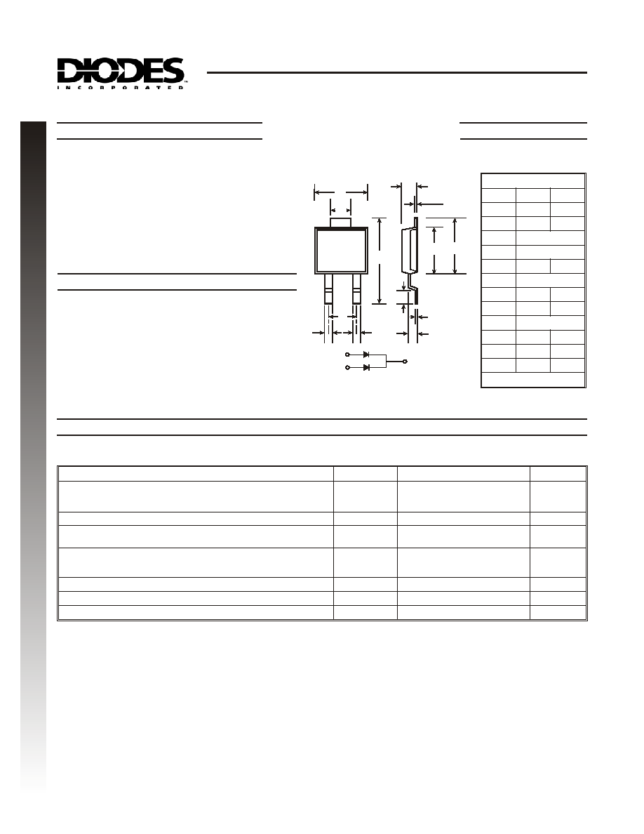
Mechanical Data
B
C
D
E
G
J
H
K
L
M
A
P
1
2
3
PIN 1
PIN 2
PIN 3, BOTTOMSIDE
HEAT SINK
C
Characteristic
Symbol
Value
Unit
Peak Repetitive Reverse Voltage
Working Peak Reverse Voltage
DC Blocking Voltage
V
RRM
V
RWM
V
R
40
V
RMS Reverse Voltage
V
R(RMS)
28
V
Average Rectified Output Current (See also Figure 5) per element
total device
I
O
5
10
A
Non-Repetitive Peak Forward Surge Current
8.3ms Single half sine-wave Superimposed on Rated Load
Per Package (JEDEC Method), total device T
C
= 115∞C
I
FSM
50
A
Typical Thermal Resistance Junction to Soldering Point Per Element
R
qJS
2.5
∞C/W
Operating Temperature Range
T
j
-55 to +125
∞C
Storage Temperature Range
T
STG
-55 to +150
∞C
∑
Guard Ring Die Construction for
Transient Protection
∑
Low Power Loss, High Efficiency
∑
High Surge Capability
∑
Very Low Forward Voltage Drop
∑
For Use in Low Voltage, High Frequency
Inverters, OR'ing, and Polarity Protection
Applications
∑
Plastic Material: UL Flammability
Classification Rating 94V-0
T
C
U
D
O
R
P
W
E
N
Maximum Ratings
@ T
A
= 25
∞C unless otherwise specified
POWERMITE
‚3
Dim
Min
Max
A
4.03
4.09
B
6.40
6.61
C
.889 NOM
D
1.83 NOM
E
1.10
1.14
G
.178 NOM
H
5.01
5.17
J
4.37
4.43
K
.178 NOM
L
.71
.77
M
.36
.46
P
1.73
1.83
All Dimensions in mm
UNDER DEVELOPMENT
DS30356 Rev. 2 - 1
2 of 3
SBM1040CT
www.diodes.com
Notes:
1. Short duration test pulse used to minimize self-heating effect.
Characteristic
Symbol
Min
Typ
Max
Unit
Test Condition
Reverse Breakdown Voltage (Note 1)
V
(BR)R
40
æ
æ
V
I
R
= 500
mA
Forward Voltage (Note 1) Per Element
V
F
æ
æ
æ
æ
0.45
0.39
0.53
0.50
0.48
0.42
0.575
0.55
V
I
F
= 5A, T
j
= 25
∞C
I
F
= 5A, T
j
= 100
∞C
I
F
= 10A, T
j
= 25
∞C
I
F
= 10A, T
j
= 100
∞C
Peak Reverse Current (Note 1)
Per Element
I
R
æ
æ
35
4
10
2
150
10
80
5
mA
mA
mA
mA
V
R
= 35V, T
j
= 25∞C
V
R
= 35V, T
j
= 100∞C
V
R
= 17.5V, T
j
= 25∞C
V
R
= 17.5V, T
j
= 100∞C
Total Capacitance Per Element
C
T
æ
375
æ
pF
f = 1.0MHz, V
R
= 4.0V DC
Electrical Characteristics
@ T
A
= 25
∞C unless otherwise specified
T
C
U
D
O
R
P
W
E
N
Ordering Information
Notes:
2. For Packaging Details, go to our website at http://www.diodes.com/datasheets/ap02007.pdf.
Device
Packaging
Shipping
SBM1040CT-13
POWERMITE
‚3
5000/Tape & Reel
(Note 2)
Marking Information
SBM1040CT = Product type marking code
= Manufacturers' code marking
YYWW = Date code marking
YY = Last digit of year ex: 2 for 2002
WW = Week code 01 to 52
YYWW
SBM1040CT
0
100
200
300
400
600
500
I
,
INST
ANT
ANE
O
US
F
O
R
W
ARD
CURRENT
(A)
F
V , INSTANTANEOUS FORWARD VOLTAGE (mV)
F
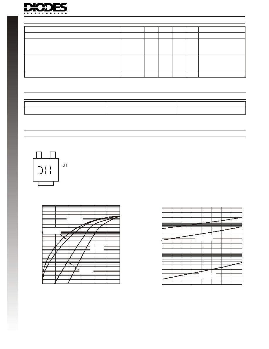
Fig. 1 Typical Forward Characteristics, Per Element
10
1
0.1
0.01
0.001
0.0001
100
T = +125∞C
j
T = +100∞C
j
T = -25∞C
j
T = +25∞C
j
0
5
10
15
20
25
30
40
35
I
,
INST
ANT
A
NE
O
US
REVERSE
CURRENT
(
m
A)
R
V , INSTANTANEOUS REVERSE VOLTAGE (V)
R
Fig. 2 Typical Reverse Characteristics, Per Element
10
1
0.1
0.01
0.001
100
T = +125∞C
j
T = +100∞C
j
T = +25∞C
j
UNDER DEVELOPMENT
DS30356 Rev. 2 - 1
3 of 3
SBM1040CT
www.diodes.com
T
C
U
D
O
R
P
W
E
N
100
1000
10,000
0
15
10
25
30
35
20
40
C
,
T
O
T
A
L
C
AP
ACIT
ANCE
(pF)
T
V , REVERSE VOLTAGE (V)
R
Fig. 4 Typical Capacitance
vs. Reverse Voltage, Per Element
5
f = 1MHz
0
1.5
3.0
4.5
7.5
6.0
0
25
50
75
100
125
150
I,
D
C
F
O
R
W
ARD
CURRENT
(A)
F
T , AMBIENT TEMPERATURE (∞C)
A
Fig. 5 DC Forward Current Derating
Note 1
Note 2
Note 3
Notes:
1. T
A
= T
SOLDERING POINT
, R
qJS
= 2.5
∞C/W, R
qSA
= 0
∞C/W.
2. Device mounted on GETEK substrate, 2"x2", 2 oz. copper, double-sided, cathode pad dimensions 0.75" x 1.0", anode pad
dimensions 0.25" x 1.0". R
qJA
in range of 20-40∞C/W.
3. Device mounted on FR-4 substrate, 2"x2", 2 oz. copper, single-sided, pad layout as per Diodes Inc. suggested pad layout
document AP02001 which can be found on our website at http://www.diodes.com/datasheets/ap02001.pdf. R
qJA
in range of
85-115∞C/W.
0
10
20
30
40
50
1
10
100
I
,
PEAK
FOR
W
A
RD
SURGE
C
URRENT
(
A)
FSM
NUMBER OF CYCLES AT 60 Hz
Fig. 3 Max Non-Repetitive Peak Fwd Surge Current
Single Half-Sine-Wave
(JEDEC Method)
T = 115∞C
C
Total Device
0
0.5
1
1.5
2.5
2
3
3.5
4
0
1
3
2
4
5
6
7
8
9
10
P
,
A
VERAGE
FOR
W
A
RD
POWER
D
ISSIP
A
T
ION
(
W)
F(A
V)
I
, AVERAGE FORWARD CURRENT (A)
F(AV)
Fig. 6 Forward Power Dissipation
T = 125∞C
j
dc
Note 3
Note 2
UNDER DEVELOPMENT
POWERMITE is a registered trademark of Microsemi Corporation.