DS11013 Rev. 13 - 2
1 of 2
SD103AW-SD103CW
SD103AW - SD103CW
SCHOTTKY BARRIER SWITCHING DIODE
Features
A
B
C
D
E
G
a
H
J
∑
Low Forward Voltage Drop
∑
Guard Ring Construction for
Transient Protection
∑
Negligible Reverse Recovery Time
∑
Case: SOD-123, Plastic
∑
Case material - UL Flammability Rating
Classification 94V-0
∑
Moisture sensitivity: Level 1 per J-STD-020A
∑
Polarity: Cathode Band
∑
Leads: Solderable per MIL-STD-202,
Method 208
∑
Marking: Date Code and Type Code, See Page 2
∑
Type Codes:
SD103AW S4
SD103BW S5 or S4
SD103CW S6 or S5 or S4
∑
Weight: 0.01 grams (approx.)
∑
Ordering Information: See Page 2
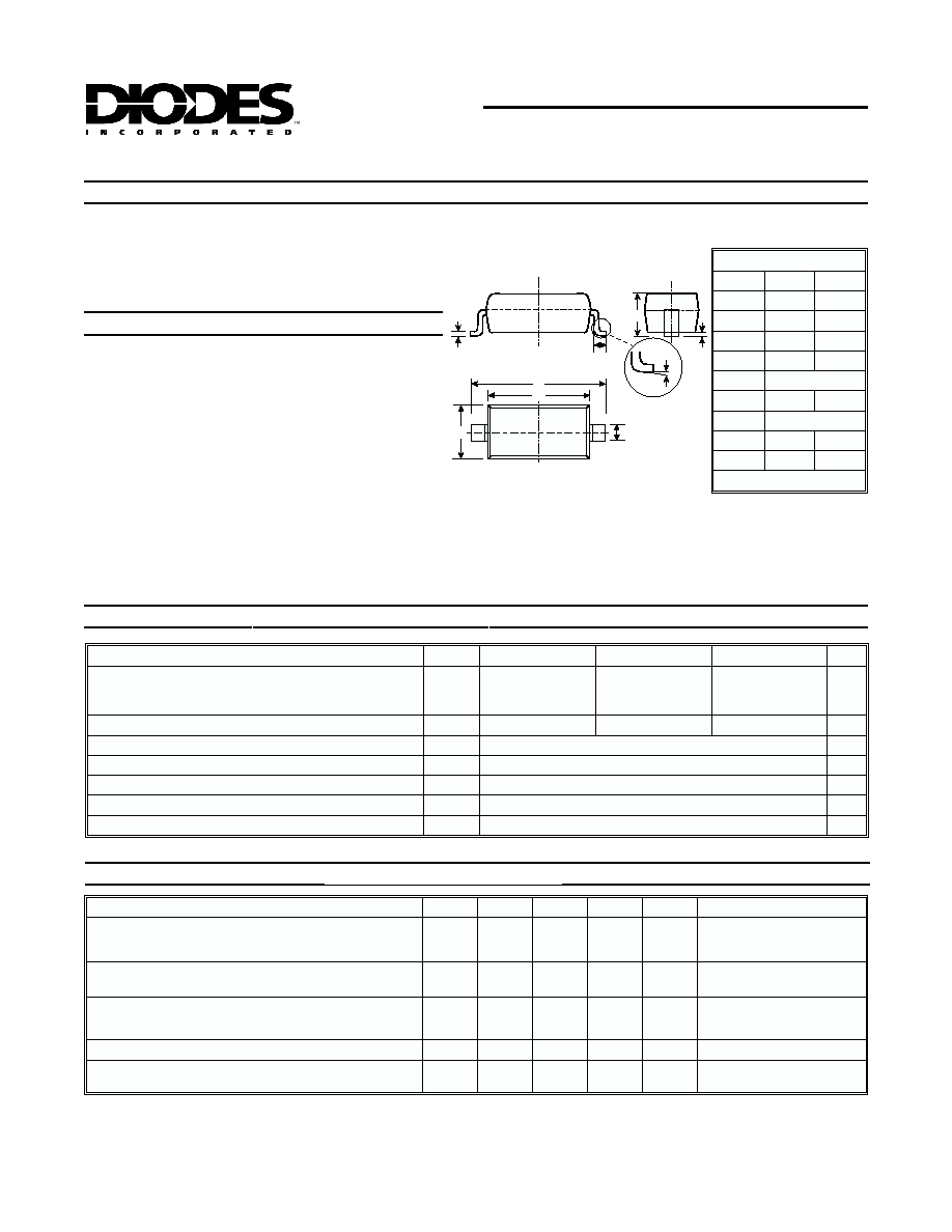
Mechanical Data
Maximum Ratings
@ T
A
= 25∞C unless otherwise specified
Notes:
1. Part mounted on FR-4 board with recommended pad layout, which can be found on our website
at http://www.diodes.com/datasheets/ap02001.pdf.
2. Short duration test pulse used to minimize self-heating effect.
Electrical Characteristics
@ T
A
= 25∞C unless otherwise specified
Characteristic
Symbol
SD103AW
SD103BW
SD103CW
Unit
Peak Repetitive Reverse Voltage
Working Peak Reverse Voltage
DC Blocking Voltage
V
RRM
V
RWM
V
R
40
30
20
V
RMS Reverse Voltage
V
R(RMS)
28
21
14
V
Forward Continuous Current (Note 1)
I
FM
350
mA
Non-Repetitive Peak Forward Surge Current @ t £ 1.0s
I
FSM
1.5
A
Power Dissipation (Note 1)
P
d
400
mW
Thermal Resistance, Junction to Ambient Air (Note 1)
R
qJA
300
∞C/W
Operating and Storage Temperature Range
T
j
, T
STG
-65 to +125
∞C
Characteristic
Symbol
Min
Typ
Max
Unit
Test Condition
Reverse Breakdown Voltage (Note 2)
SD103AW
SD103BW
SD103CW
V
(BR)R
40
30
20
æ
æ
V
I
R
= 100mA
Forward Voltage Drop (Note 2)
V
FM
æ
æ
0.37
0.60
V
I
F
= 20mA
I
F
= 200mA
Peak Reverse Current (Note 2)
SD103AW
SD103BW
SD103CW
I
RM
æ
æ
5.0
mA
V
R
= 30V
V
R
= 20V
V
R
= 10V
Total Capacitance
C
T
æ
50
æ
pF
V
R
= 0V, f = 1.0MHz
Reverse Recovery Time
t
rr
æ
10
æ
ns
I
F
= I
R
= 200mA,
I
rr
= 0.1 x I
R
, R
L
= 100W
SOD-123
Dim
MinMax
A
3.55
3.85
B
2.55
2.85
C
1.40
1.70
D
--
1.35
E
0.55 Typical
G
0.25
--
H
0.11 Typical
J
--
0.10
a
0∞
8∞
All Dimensions in mm
DS11013 Rev. 13 - 2
2 of 2
SD103AW-SD103CW
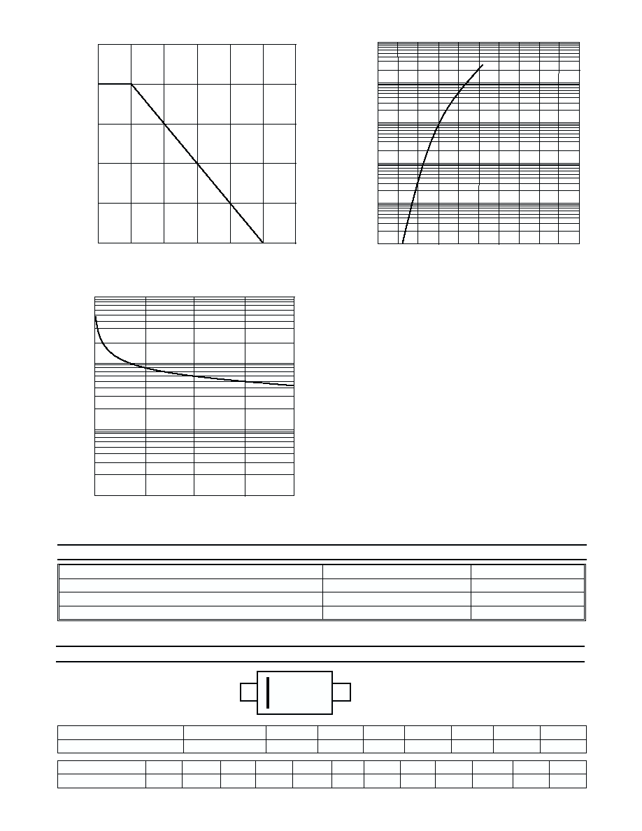
0
100
200
500
0
25
50
75
125
150
P,
P
O
WER
DISSIP
AT
I
O
N
(mW)
d
T , AMBIENT TEMPERATURE (∞C)
Fig.1 Power Derating Curve
A
100
300
400
1.0
10
100
1000
0.10
0.01
0
0.5
1.0
I
,
FOR
W
A
RD
CURRENT
(
mA)
F
V , FORWARD VOLTAGE (V)
Fig. 2 Typical Forward Characteristics
F
C,
T
O
T
A
L
CAP
ACIT
ANCE
(pF)
T
V , REVERSE VOLTAGE (V)
R
Fig. 3 Typ. Total Capacitance vs Reverse Voltage
100
0.1
1.0
10
0
10
20
30
40
Month
Jan
Feb
March
Apr
May
Jun
Jul
Aug
Sep
Oct
Nov
Dec
Code
1
2
3
4
5
6
7
8
9
O
N
D
Year
1998
1999
2000
2001
2002
2003
2004
2005
Code
J
K
L
M
N
P
R
S
Date Code Key
XX = Product Type Marking Code
YM = Date Code Marking
Y = Year (ex: N = 2002)
M = Month (ex: 9 = September)
XX
YM
Marking Information
Note:
3. For Packaging Details, go to our website at http://www.diodes.com/datasheets/ap02007.pdf.
Ordering Information
Device
Packaging
Shipping
SD103AW-7
SOD-123
3000/Tape and Reel
SD103BW-7
SOD-123
3000/Tape and Ree
SD103CW-7
SOD-123
3000/Tape and Ree
(Note 3)