
DS30359 Rev. 2 - 1
1 of 4
TB0640L - TB3500L
TB0640L - TB3500L
30A BI-DIRECTIONAL SURFACE MOUNT THYRISTOR
SURGE PROTECTIVE DEVICE
Features
∑
30A Peak Pulse Current @ 10/1000ms
∑
150A Peak Pulse Current @ 8/20ms
∑
58 - 320V Stand-Off Voltages
∑
Oxide-Glass Passivated Junction
∑
Bi-Directional Protection In a Single Device
∑
High Off-State impedance and Low On-State
Voltage
Mechanical Data
∑
Case: SMB, Molded Plastic
∑
Plastic Material: UL Flammability
Classification Rating 94V-0
∑
Moisture sensitivity: Level 1 per J-STD-020A
∑
Terminals: Solder Plated Terminal -
Solderable per MIL-STD-202, Method 208
∑
Polarity: None; Bi-Directional Devices Have No
Polarity Indicator
∑
Weight: 0.093 grams (approx.)
∑
Marking: Date Code and Marking Code (See Page 4)
∑
Ordering Information: See Page 4
Single phase, half wave, 60Hz, resistive or inductive load.
For capacitive load, derate current by 20%.
B
A
C
D
F
H
E
G
Characteristic
Symbol
Value
Unit
Non-Repetitive Peak Impulse Current @10/1000us
I
pp
30
A
Non-Repetitive Peak On-State Current @8.3ms (one-half cycle)
I
TSM
15
A
Junction Temperature Range
T
j
-40 to +150
∞
C
Storage Temperature Range
T
STG
-55 to +150
∞
C
Thermal Resistance, Junction to Lead
R
q
JL
30
∞C/W
Thermal Resistance, Junction to Ambient
R
q
JA
120
∞C/W
Typical Positive Temperature Coefficient for Breakdown Voltage
D
VBR/DT
j
0.1
%/∞C
SMB
Dim
Min
Max
A
4.06
4.57
B
3.30
3.94
C
1.96
2.21
D
0.15
0.31
E
5.21
5.59
F
0.05
0.20
G
2.01
2.62
H
0.76
1.52
All Dimensions in mm
Maximum Ratings
@ T
A
= 25∞C unless otherwise specified
Maximum Rated Surge Waveform
Waveform
Standard
Ipp (A)
2/10 us
GR-1089-CORE
200
8/20 us
IEC 61000-4-5
150
10/160 us
FCC Part 68
100
10/700 us
ITU-T, K20/K21
60
10/560 us
FCC Part 68
50
10/1000 us
GR-1089-CORE
30
0
TIME
100
50
0
I
,
P
E
A
K
P
U
L
S
E
C
U
R
R
E
N
T
(
%
)
P
P
Peak Value (I )
pp
Half Value
t = rise time to peak value
r
t = decay time to half value
p
t
r
t
p
T
C
U
D
O
R
P
W
E
N
UNDER DEVELOPMENT

DS30359 Rev. 2 - 1
2 of 4
TB0640L - TB3500L
Electrical Characteristics
@ T
A
= 25∞C unless otherwise specified
Part Number
Rated
Repetitive
Off-State
Voltage
Off-State
Leakage
Current @
V
DRM
Breakover
Voltage
On-State
Voltage
@ I
T
= 1A
Breakover
Current
I
BO
Holding Current
I
H
Off-State
Capacitance
Marking
Code
V
DRM
(V)
I
DRM
(uA)
V
BO
(V)
V
T
(V)
Min
(mA)
Max (mA)
Min
(mA)
Max (mA)
C
O
(pF)
TB0640L
58
5
77
3.5
50
800
150
800
100
T064L
TB0720L
65
5
88
3.5
50
800
150
800
100
T072L
TB0900L
75
5
98
3.5
50
800
150
800
100
T090L
TB1100L
90
5
130
3.5
50
800
150
800
60
T110L
TB1300L
120
5
160
3.5
50
800
150
800
60
T130L
TB1500L
140
5
180
3.5
50
800
150
800
60
T150L
TB1800L
160
5
220
3.5
50
800
150
800
60
T180L
TB2300L
190
5
265
3.5
50
800
150
800
40
T230L
TB2600L
220
5
300
3.5
50
800
150
800
40
T260L
TB3100L
275
5
350
3.5
50
800
150
800
40
T310L
TB3500L
320
5
400
3.5
50
800
150
800
40
T350L
Symbol
Parameter
V
DRM
Stand-off Voltage
I
DRM
Leakage current at stand-off voltage
V
BR
Breakdown voltage
I
BR
Breakdown current
V
BO
Breakover voltage
I
BO
Breakover current
I
H
Holding current NOTE: 1
V
T
On state voltage
I
PP
Peak pulse current
C
O
Off-state capacitance NOTE: 2
Notes:
1. I
H
> (V
L
/R
L
) If this criterion is not obeyed, the TSPD triggers but does not return correctly to high-resistance state. The surge
recovery time does not exceed 30ms.
2. Off-state capacitance measured at f = 1.0MHz, 1.0V
RMS
signal, V
R
= 2V
DC
bias.
I
BO
V
BR
V
DRM
V
T
V
BO
I
H
I
V
I
BR
I
DRM
I
PP
T
C
U
D
O
R
P
W
E
N
UNDER DEVELOPMENT
DS30359 Rev. 2 - 1
3 of 4
TB0640L - TB3500L
0.9
T , JUNCTION
J
TEMPERATURE (∞C)
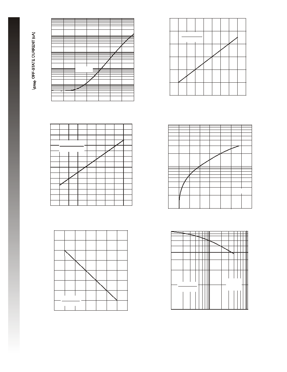
Fig. 2 Relative Variation of Breakdown Voltage
vs. Junction Temperature
V
= (T )
BR
J
V
= (T = 25∞C)
BR J
0.95
1
1.05
1.1
1.15
1.2
-50
-25
0
25
50
75
100 125 150 175
N
O
R
M
A
L
I
Z
E
D
B
R
E
A
K
D
O
W
N
V
O
L
T
A
G
E
1
10
100
1
2
5
4
3
7
6
9
8
I
,
O
N
-
S
T
A
T
E
C
U
R
R
E
N
T
(
A
)
T
V , ON-STATE VOLTAGE (V)
T
Fig. 4 On-State Current vs. On-State Voltage
T = 25∞C
j
0
0.5
1
1.5
2
-50
-25
0
25
50
100
75
125
N
O
R
M
A
L
I
Z
E
D
H
O
L
D
I
N
G
C
U
R
R
E
N
T
T , JUNCTION TEMPERATURE (∞C)
J
Fig. 5 Relative Variation of Holding Current vs.
Junction Temperature
I = (T )
H J
I
= (T = 25∞C)
H
J
0.1
1
1
10
100
N
O
R
M
A
L
I
Z
E
D
C
A
P
A
C
I
T
A
N
C
E
V , REVERSE VOLTAGE (V)
R
Fig. 6 Relative Variation of Junction Capacitance
vs. Reverse Voltage Bias
C = (V )
O
R
C
= (V = 1V)
O
R
T = 25∞C
j
f = 1 Mhz
V
RMS
= 1V
T
C
U
D
O
R
P
W
E
N
UNDER DEVELOPMENT
1
1.05
0.95
-50
N
O
R
M
A
L
I
Z
E
D
B
R
E
A
K
D
O
W
N
V
O
L
T
A
G
E
T , JUNCTION TEMPERATURE (∫C)
J
Fig. 3 Relative Variation of Breakover Voltage
vs. Junction Temperature
1.1
-25
0
75
50
25
125
100
175
150
V
= (T )
BO
J
V
= (T = 25∞C)
BO J
T , JUNCTION TEMPERATURE (∞C)
J
Fig. 1 Off-State Current vs. Junction Temperature
0.001
0.01
1
0.1
10
100
-25
0
25
50
75
100
125
150
V
= 50V
DRM
