
2 Megabit SRAM / 8 Megabit FLASH
DP3SZ128512X16NY5
ADVANCED INFORMATION
DESCRIPTION:
The DP3SZ128512X16NY5 modules are a
revolutionary new memory subsystem using
Dense-Pac Microsystems' TSOP stacking
technology. The Module packs 2-Megabits of
CMOS SRAM and 8-Megabits of FLASH EEPROM
in an area of 0.546 in
2
, while maintaining a total
height of .094 inches maximum.
The DP3SZ128512X16NY5 module contains two
individual TSOP packages, one TSOP containing a
128Kx16 SRAM memory device and one TSOP
containing a 512Kx16 Simultaneous Operation
FLASH memory device.
Using the TSOP Stack family of modules offer a
higher board density of memory than available with
conventional through-hole, surface mount or
hybrid techniques.
FEATURES:
∑
Access Time:
70ns
∑
Single 3.3 Volt Supply
∑
Fully Static Operation - No clock or refresh required
∑
Simultaneous Read/Write FLASH Operation
∑
Top or Bottom BOOT Block Configuration Available
∑
TTL Compatible Inputs and Outputs
∑
Common Data Inputs and Outputs
∑
10,000 Erase/Program Cycles (min.)
∑
Package: 56-Pin TSOP Stack
FUNCTIONAL BLOCK DIAGRAM
PIN NAMES
A0 - A18
Address Inputs
I/O0 - I/O15
Data Input/Output
FCS
FLASH Chip Enable
RAMCS
SRAM Low Chip Enable
UB
Upper Byte (SRAM)
LB
Lower Byte (SRAM)
BYTE
Select 8-Bit or
16-Bit Mode (FLASH)
RY/BY
Ready/Busy Output
(FLASH)
WE
Write Enable
OE
Output Enable
RESET
Reset
V
DD
Power (+5V)
V
SS
Ground
N.C.
No Connect
2Meg SRAM/8Meg FLASH, 70ns, TSOP STACK
30A193-00
C
This document contains information on a product under consideration for
development at Dense-Pac Microsystems, Inc. Dense-Pac reserves the right
to change or discontinue information on this product without prior notice.
PIN-OUT DIAGRAM
30A193-00
REV. C
1

DP3SZ128512X16NY5
Dense-Pac Microsystems, Inc.
ADVANCED INFORMATION
BUS OPERATIONS
Mode
RAMCS FCS LB
UB OE WE BYTE
RESET
Address
I/O0-
I/O7
I/O8-
I/O15
Supply
Current
Read SRAM (LB)
L
H
L
H
L
H
X
V
CC
±
0.3V
A
IN
D
OUT
High-Z
I
CC1
Read SRAM (UB)
L
H
H
L
L
H
X
V
CC
±
0.3V
A
IN
High-Z
D
OUT
I
CC1
Read SRAM (Word)
L
H
L
L
L
H
X
V
CC
±
0.3V
A
IN
D
OUT
D
OUT
I
CC1
Write SRAM (LB)
L
H
L
H
X
L
X
V
CC
±
0.3V
A
IN
D
IN
High-Z
I
CC1
Write SRAM (UB)
L
H
H
L
X
L
X
V
CC
±
0.3V
A
IN
High-Z
D
IN
I
CC1
Write SRAM (Word)
L
H
L
L
X
L
X
V
CC
±
0.3V
A
IN
D
IN
D
IN
I
CC1
Read FLASH (Byte)
H
L
X
X
L
H
L
H
A
IN
D
OUT
I/O8-I/O14
=High-Z,
I/O15=A-1
I
CC2
Read FLASH (Word)
H
L
X
X
L
H
H
H
A
IN
D
OUT
D
OUT
I
CC2
Write FLASH (Byte)
H
L
X
X
H
L
L
H
A
IN
D
IN
I/O8-I/O14
=High-Z,
I/O15=A-1
I
CC3
Write FLASH (Word)
H
L
X
X
H
L
H
H
A
IN
D
IN
D
IN
I
CC3
Standby
H
H
X
X
X
X
X
V
CC
±
0.3V
X
High-Z
High-Z
I
SB
Output Disable
SRAM Active
L
H
X
X
H
H
X
V
CC
±
0.3V
X
High-Z
High-Z
I
CC1
L
H
H
H
X
X
X
Output Disable
FLASH Active
H
L
X
X
H
H
X
H
X
High-Z
High-Z
I
CC2
FLASH Sector Protect
H
L
X
X
H
L
X
V
ID
Sector
Address
A6=L
A1=H
A0=L
D
IN
X
I
CC2
FLASH Sector Unprotect
H
L
X
X
H
L
X
V
ID
Sector
Address
A6=H
A1=H
A0=L
D
IN
X
I
CC2
FLASH Temporary Sector
Unprotect (Byte)
H
L
X
X
X
X
L
V
ID
A
IN
D
IN
High-Z
I
CC2
FLASH Temporary Sector
Unprotect (Word)
H
L
X
X
X
X
H
V
ID
A
IN
D
IN
D
IN
I
CC2
RECOMMENDED OPERATING RANGE
3
Symbol
Characteristic
Min.
Max.
Unit
V
CC
Supply Voltage
3.0
3.6
V
V
SS
Ground
0
0
V
IH
Input HIGH
Voltage
0.7 x V
CC
,
2.2 min.
V
CC
+0.2
V
V
IL
Input LOW
Voltage
-0.2
0.4
V
ABSOLUTE MAXIMUM RATINGS
3
Symbol
Parameter
Value
Unit
T
STC
Storage Temperature
-65 to +150
∞
C
T
A
Temperature Under Bias
-0 to +70
∞
C
V
DD
Supply Voltage
1
-0.5 to +4.0
∞
C
V
I/O
Input/Output Voltage
1
-0.2 to 3.9
V
30A193-00
REV. C
2

Dense-Pac Microsystems, Inc.
DP3SZ128512X16NY5
ADVANCED INFORMATION
CAPACITANCE
4
:
T
A
= 25∞C, F = 1.0MHz
Symbol
Parameter
Max.
Condition
Unit
C
IN
Input
20
V
IN
= 0V
pF
C
I/O
Data Input/Output
25
V
I/O
= 0V
pF
+2.8V
3.1K
3.0K
C
L
*
D
OUT
Figure 1.
Output Load
* Including Probe and Jig Capacitance.
TEST CONDITIONS
Input Pulse Levels
0V to 3.0V
Input Pulse Rise and Fall Times
5ns
Input and Output Timing Reference Levels 1.5V
Output Load
C
L
= 30pF
DC OPERATING CHARACTERISTICS
Symbol
Characteristic
Test Conditions
Min.
Typ.
Max.
Unit
I
IN
Input Leakage Current
V
IN
= V
SS
to V
CC
-2
2
µ
A
I
OUT
Output Leakage Current
RAMCS=FCS=V
IH
, V
I/O
=V
SS
to V
CC
-2
2
µ
A
I
CC1
Operating Current - SRAM
Cycle=Min., Duty=100%,
I
OUT
=0mA
70
mA
I
CC2
Operating Current - FLASH Read
FCS=V
IL
, OE=V
IH
7
12
mA
I
CC3
Operating Current - FLASH Write
FCS=V
IL
, OE=V
IH
, WE=V
IL
15
30
mA
I
CC4
Operating Current - FLASH
Read-While-Write
FCS=V
IL
, OE=V
IH
21
45
mA
I
CC5
Operating Current - FLASH
Read-While-Erase
FCS=V
IL
, OE=V
IH
21
45
mA
I
CC6
Operating Current - FLASH
Read-While-Erase-Suspended
FCS=V
IL
, OE=V
IH
17
35
ma
I
SB1
Standby Current (TTL)
RAMCS=FCS=V
IH
, V
IN
=V
IH
or V
IL
2
mA
I
SB2
Standby Current (CMOS)
RAMCS=FCS=V
CC
±
0.2V,
RESET=V
SS
±
0.3V
15
µ
A
V
ID
Voltage for Sector Protect/Unprotect
11.5
12.5
V
V
LKO
Low V
CC
Lock-Out-Protect
2.3
2.5
V
V
OL
Output Low Voltage
I
OL
=2.1mA, V
CC
=V
CC
min.
0.4
V
V
OH
Output High Voltage
I
OH
= -1.0mA
2.4
V
SRAM; DATA RETENTION CHARACTERISTICS
(t
A
= 0 to 70∞C, unless otherwise specified)
Symbol
Item
Test Condition
Min.
Max.
Units
V
DR
V
CC
for Data Retention
RAMCS = V
CC
-0.2V
1.5
3.6
V
t
SDR
Data Retention Set-up Time
See Data Retention Waveform
0
ns
t
RDR
Recovery Time
See Data Retention Waveform
t
RC
ns
30A193-00
REV. C
3

DP3SZ128512X16NY5
Dense-Pac Microsystems, Inc.
ADVANCED INFORMATION
SRAM - READ PARAMETERS
Symbol
Parameter List
Min.
Max.
Units
t
RC
Read Cycle Time
70
ns
t
AA
Address Access Time
70
ns
t
CO
Chip Select to Output
70
ns
t
OE
Output Enable to Valid Output
35
ns
t
BA
UB, LB Access Time
35
ns
t
LZ
Chip Select to Low-Z Output
10
ns
t
OLZ
Output Enable to Low-Z Output
5
ns
t
BLZ
UB, LB to Low-Z Output
5
ns
t
HZ
Chip Disable to High-Z Output
0
25
ns
t
OHZ
Output Enable disable to High-Z
0
25
ns
t
BHZ
UB, LB disable to High-Z
0
25
ns
t
OH
Output Hold from Address Change
10
ns
SRAM - WRITE PARAMETERS
Symbol
Parameter List
Min.
Max.
Units
t
WC
Write Cycle Time
70
ns
t
CW
Chip Select to End of Write
65
ns
t
AS
Address Setup Time
0
ns
t
AW
Address Valid to End of Write
65
ns
t
WP
Write Pulse Width
55
ns
t
BW
UB, LB Valid to End of Write
65
ns
t
WR
Write Recovery
0
ns
t
WHZ
Write to High-Z Output
0
25
ns
t
DW
Data to Write Time Overlap
30
ns
t
DH
Data Hold form Write Time
0
ns
t
OW
End Write to Output in Low-Z
5
ns
SRAM; DATA RETENTION WAVEFORM:
RAMCS Controlled.
V
CC
V
IH
V
DR
RAMCS
V
SS
30A193-00
REV. C
4

Dense-Pac Microsystems, Inc.
DP3SZ128512X16NY5
ADVANCED INFORMATION
SRAM; READ CYCLE 1:
Address Controlled. RAMCS = OE = V
IL
, WE = V
IH
, UB and/or LB = V
IL
, FSC = V
IH
SRAM; READ CYCLE 2:
WE = V
IH
, FCS = V
IH
ADDRESS
RAMCS
UB/LB
OE
DATA OUT
ADDRESS
DATA OUT
SRAM; READ CYCLE NOTES:
1. t
HZ
and t
OHZ
are defined as the time at which the outputs achieve the open circuit conditions and are not referenced to output
voltage levels.
2. At any given time temperature and voltage conditions, t
HZ
(max.) is less than t
LZ
(min.) both for a given device and from device
to device.
30A193-00
REV. C
5

DP3SZ128512X16NY5
Dense-Pac Microsystems, Inc.
ADVANCED INFORMATION
SRAM; READ CYCLE 2:
CE Controlled. FCS = V
IH
ADDRESS
RAMCS
UB/LB
WE
DATA IN
DATA OUT
SRAM: WRITE CYCLE 1:
WE Controlled. FCS = V
IH
ADDRESS
RAMCS
UB/LB
WE
DATA IN
DATA OUT
30A193-00
REV. C
6

Dense-Pac Microsystems, Inc.
DP3SZ128512X16NY5
ADVANCED INFORMATION
SRAM; READ CYCLE 3:
UL, LB Controlled. FCS = V
IH
SRAM; WRITE CYCLE NOTES:
1. A write occurs during the overlap (t
WP
) of a low RAMCS and Low WE. A write begins at the latest transition among RAMCS
going Low and WE going Low. : A write end at the earliest transition among RAMCS going High and WE going High, t
WP
is
measured from the beginning of write to the end of write.
2. t
CW
is measured from the later of RAMCS going Low to end of write.
3. t
AS
is measured for the address valid to the beginning of write.
4. t
WR
is measured form the end of write to the address change. t
WR
applied in case a write ends as
RAMCS, or WE going High.
ADDRESS
RAMCS
UB/LB
WE
DATA OUT
DATA IN
30A193-00
REV. C
7

DP3SZ128512X16NY5
Dense-Pac Microsystems, Inc.
ADVANCED INFORMATION
FLASH Simultaneous Read/Write Operations
with Zero Latency
The Simultaneous Read/Write architecture provides
simultaneous operation by dividing the memory space into
two banks. Bank 1 contains eight boot/parameter sectors, and
Bank 2 consists of fourteen larger, code sectors of uniform size.
The device can improve overall system performance by
allowing a host system to program or erase in one bank, then
immediately and simultaneously read from the other bank,
with zero latency. This releases the system from waiting for
the completion of program or erase operations.
FLASH Word/Byte Configuration
The BYTE pin controls whether the device data I/O pins
operate in the byte or word configuration. If the BYTE pin is
set at logic `1', the device is in word configuration, I/O0-I/O15
are active and controlled by FCS and OE.
If the BYTE pin is set at logic `0', the device is in byte
configuration, and only data I/O pins I/O0-I/O7 are active and
controlled by FCS and OE. The data I/O pins I/O8-I/O14 are
tri-stated, and the I/O15 pin is used as an input for the LSB
(A-1) address function.
Requirements for Reading, FLASH Array Data
To read array data from the outputs, the system must drive the
FCS and OE pins to V
IL
. Is the power control and selects the
device. OE is the output control and gates array data to the
output pins. WE should remain at V
IH
. The BYTE pin
determines whether the device outputs array data in words or
bytes.
The internal state machine is set for reading array data upon
device power-up, or after a hardware reset. This ensures that
no spurious alteration of the memory content occurs during
the power transition. No command is necessary in this mode
to obtain array data. Standard microprocessor read cycles that
assert valid addresses on the device address inputs produce
valid data on the device data outputs. Each bank remains
enabled for read access until the command register contents
are altered.
Table 1. FLASH TOP BOOT SECTOR ARCHITECTURE
Bank
Sector
Sector Address
Sector Size
(Kbytes/
Kwords)
(x8)
Address Range
(x16)
Address Range
Bank Address
A15
A14
A13
A12
A18
A17
A16
Bank 2
SA0
0
0
0
0
X
X
X
64/32
00000h-0FFFFh
00000h-07FFFh
SA1
0
0
0
1
X
X
X
64/32
10000h-1FFFFh
08000h--FFFFh
SA2
0
0
1
0
X
X
X
64/32
20000h-2FFFFh
10000h-17FFFh
SA3
0
0
1
1
X
X
X
64/32
30000h-3FFFFh
18000h-1FFFFh
SA4
0
1
0
0
X
X
X
64/32
40000h-4FFFFh
20000h-27FFFh
SA5
0
1
0
1
X
X
X
64/32
50000h-5FFFFh
28000h-2FFFFh
SA6
0
1
1
0
X
X
X
64/32
60000h-6FFFFh
30000h-37FFFh
SA7
0
1
1
1
X
X
X
64/32
70000h-7FFFFh
38000h-3FFFFh
SA8
1
0
0
0
X
X
X
64/32
80000h-8FFFFh
40000h-47FFFh
SA9
1
0
0
1
X
X
X
64/32
90000h-9FFFFh
48000h-4FFFFh
SA10
1
0
1
0
X
X
X
64/32
A0000h-AFFFFh
50000h-57FFFh
SA11
1
0
1
1
X
X
X
64/32
B0000h-BFFFFh
58000h-5FFFFh
SA12
1
1
0
0
X
X
X
64/32
C0000h-CFFFFh
60000h-67FFFh
SA13
1
1
0
1
X
X
X
64/32
D0000h-DFFFFh
68000h-6FFFFh
Bank 1
SA14
1
1
1
0
0
0
X
16/8
E000h-E3FFFh
70000h-71FFFh
SA15
1
1
1
0
0
1
X
32/16
E4000h-E7FFFh,
E8000h-EBFFFh
72000h-73FFFh,
74000h-75FFFh
1
0
X
SA16
1
1
1
0
1
1
0
8/4
EC000h-EDFFFh
76000h-76FFFh
SA17
1
1
1
0
1
1
1
8/4
EE000h-EFFFFh
77000h-77FFFh
SA18
1
1
1
1
0
0
0
8/4
F0000h-F1FFFh
78000h-78FFFh
SA19
1
1
1
1
0
0
1
8/4
F2000h-F3FFFh
79000h-79FFFh
SA20
1
1
1
1
0
1
X
32/16
F4000h-F7FFFh,
F8000h-FBFFFh
7A000h-7BFFFh,
7C000h-7DFFFh
1
0
X
SA21
1
1
1
1
1
1
X
16/8
FC000h-FFFFFh
7E000h-7FFFFh
NOTE:
The address range is A18:A-1 if in byte mode (BYTE - V
IL
). The address range is A18:A0 if in word mode (BYTE=V
IH
).
30A193-00
REV. C
8

Dense-Pac Microsystems, Inc.
DP3SZ128512X16NY5
ADVANCED INFORMATION
Writing Commands/Command Sequences
To write a command or command sequence (which includes
programming data to the device and erasing sectors of
memory), the system must drive WE and FCS to V
IL
, and OE
to V
IH
. For program operations, the BYTE pin determines
whether the device accepts program data in bytes or words.
Refer to "Word/Byte Configuration" for more information.
The device features an Unlock Bypass mode to facilitate faster
programming. Once a bank enters the Unlock Bypass mode,
only two write cycles are required to program a word or byte,
instead of four. The "Byte/Word Program Command
Sequence" section has details on programming data to the
device, using both standard and Unlock Bypass command
sequences.
An erase operation can erase one sector, multiple sectors, or
the entire device. Tables 1 and 2 indicate the address space
that each sector occupies. The device address space is divided
into two banks: Bank 1 contains the boot/parameter sectors,
and Bank 2 contains the larger, code sectors of uniform size.
A "bank address" is the address bits required to uniquely select
a bank. Similarly, a "sector address" is the address bits
required to uniquely select a sector.
If the system writes the autoselect command sequence, the
device enters the autoselect mode. The system can then read
autoselect, codes from the internal register (which is separate
from the memory array) on I/O7-I/O0. Standard read cycle
timings apply in this mode. Refer to the Autoselect Mode and
Autoselect. Command Sequence sections for more
information.
Simultaneous Read/Write Operations with Zero Latency
This device is capable of reading data from one bank of
memory while programming or erasing in the other bank of
memory. An erase operation may also be suspended to read
from or program to another location within the same bank
(except the sector being erased). Figure 13 shows how read
and write cycles may be initiated for simultaneous operation
with zero latency.
Table 2. FLASH BOTTOM BOOT SECTOR ARCHITECTURE
Bank
Sector
Sector Address
Sector Size
(Kbytes/
Kwords)
(x8)
Address Range
(x16)
Address Range
Bank Address
A15
A14
A13
A12
A18
A17
A16
Bank 2
SA21
1
1
1
1
X
X
X
64/32
F0000h-FFFFFh
78000h-7FFFFh
SA20
1
1
1
0
X
X
X
64/32
E0000h-EFFFFh
70000h--77FFh
SA19
1
1
0
1
X
X
X
64/32
D0000h-DFFFFh
68000h-6FFFFh
SA18
1
1
0
0
X
X
X
64/32
C0000h-CFFFFh
60000h-67FFFh
SA17
1
0
1
1
X
X
X
64/32
B0000h-BFFFFh
58000h-5FFFFh
SA16
1
0
1
0
X
X
X
64/32
A0000h-AFFFFh
50000h-57FFFh
SA15
1
0
0
1
X
X
X
64/32
90000h-9FFFFh
48000h-4FFFFh
SA14
1
0
0
0
X
X
X
64/32
80000h-8FFFFh
40000h-47FFFh
SA13
0
1
1
1
X
X
X
64/32
70000h-7FFFFh
38000h-3FFFFh
SA12
0
1
1
0
X
X
X
64/32
60000h-6FFFFh
30000h-37FFFh
SA11
0
1
0
1
X
X
X
64/32
50000h-5FFFFh
28000h-2FFFFh
SA10
0
1
0
0
X
X
X
64/32
40000h-4FFFFh
20000h-27FFFh
SA9
0
0
1
1
X
X
X
64/32
30000h-3FFFFh
18000h-1FFFFh
SA8
0
0
1
0
X
X
X
64/32
20000h-2FFFFh
10000h-17FFFh
Bank 1
SA7
0
0
0
1
1
1
X
16/8
1C000h-1FFFFh
0E000h-0FFFFh
SA6
0
0
0
1
1
0
X
32/16
18000h-1BFFFh,
14000h-17FFFh
0C000h-0DFFFh,
0A000h-0BFFFh
0
1
X
SA5
0
0
0
1
0
0
1
8/4
12000h-13FFFh
09000h-09FFFh
SA4
0
0
0
1
0
0
0
8/4
10000h-11FFFh
08000h-08FFFh
SA3
0
0
0
0
1
1
1
8/4
0E000h-0FFFFh
07000h-07FFFh
SA2
0
0
0
0
1
1
0
8/4
0C000h-0DFFFh
06000h-06FFFh
SA1
0
0
0
0
1
0
X
32/16
08000h-0BFFFh,
04000h-07FFFh
04000h-05FFFh,
02000h-03FFFh
0
1
X
SA0
0
0
0
0
0
0
X
16/8
00000h-03FFFh
00000h-01FFFh
NOTE:
The address range is A18:A-1 if in byte mode (BYTE - V
IL
). The address range is A18:A0 if in word mode (BYTE=V
IH
).
30A193-00
REV. C
9

DP3SZ128512X16NY5
Dense-Pac Microsystems, Inc.
ADVANCED INFORMATION
Standby Mode
When the system is not reading or writing to the device, it can
place the device in the standby mode. In this mode, current
consumption is greatly reduced, and the outputs are placed in
the high impedance state, independent of the OE input.
The device enters the CMOS standby mode when the OE and
RESET pins are all held at V
CC
±
0.2V (Note that this is a more
restricted voltage range than V
IH
.) If FCS and RESET are held
at V
IH
, but not within V
CC
±
0.2V, the device will be in the
standby mode, but the standby current will be greater. The
device requires standard access time (t
CE
) for read access when
the device is in either of these standby modes, before it is ready
to read data.
If the device is deselected during erasure or programming, the
device draws active current until the operation is completed.
RESET: Hardware Reset Pin
The RESET pin provides a hardware method of resetting the
device to reading array data. When the RESET pin is driven
low for at least a period of t
RP
, the device immediately
terminates any operation in progress, tristates all output pins,
and ignores all read/write commands for the duration of the
RESET pulse. The device also resets the internal state machine
to reading array data. The operation that was interrupted
should be reinitiated once the device is ready to accept another
command sequence, to ensure data integrity.
Current is reduced for the duration of the RESET pulse. When
RESET is held at V
SS
±
0.3 V, the device draws CMOS standby
current I
SB2
. If RESET is held at V
IL
but not within V
SS
±
0.3 the
standby current will be greater.
The RESET pin may be tied to the system reset circuitry. A
system reset would thus also reset the Flash memory, enabling
the system to read the boot-up firmware from the Flash
memory.
If RESET is asserted during a program or erase operation, the
RY/BY pin remains a "0" (busy) until the internal reset operation
is complete, which requires a time of ready (during Embedded
Algorithms). The system can thus monitor RY/BY to determine
whether the reset operation is complete. If RESET is asserted
when a program or erase operation is not executing (RY/BY pin
is "1"), the reset operation is completed within a time of ready
(not during Embedded Algorithms). The system can read date
t
RH
after the RESET pin returns to V
IH
.
Output Disable Mode
When the OE input is a V
IH
, output from the device is disabled.
The output pins are placed in the high impedance state.
Autoselect Mode
The autoselect mode provides manufacturer and device
identification, and sector protection verification, through
identifier codes output on I/O7-I/O0. The autoselect codes
can be accessed in-system through the command register.
To access the autoselect codes in-system, the host system can
issue the autoselect, the host system can issue the autoselect
command via the command register, as shown in Table 3.
Sector Protection/Unprotection
The hardware sector protection feature disables both program
and erase operations in any sector. The hardware sector
unprotection feature re-enables both program and erase
operations in previously protected sectors.
The Sector Protection/Unprotection method requires V
ID
on
the RESET pin only, and can be implemented either in-system
or via programming equipment. Figure 1 shows the algorithms
and Figure 18 shows the timing diagram. This method uses
standard microprocessor bus cycle timing. For sector
unprotect, all unprotected sectors must first be protected prior
to the first sector unprotect write cycle.
The device is shipped with all sectors unprotected. AMD offers
the option of programming and protecting sectors at its factory
prior to shipping.
It is possible to determine whether a sector is protected or
unprotected. See the Autoselect Mode section for details.
Temporary Sector Unprotect
This feature allows temporary unprotection of previously
protected sectors to change data in- system. The Sector
Unprotect mode is activated by setting the RESET pin to V
ID
(11.5 V-12.5 V). During this mode, formerly protected sectors
can be programmed or erased by selecting the sector
addresses. Once V
ID
is removed from the RESET # pin, all
the previously protected sectors are protected again. Figure 1
shows the algorithm, and Figure 17 shows the timing diagrams,
for this feature.
Figure 1. Temporary Sector Unprotect Operation
NOTES:
1. All protected sectors unprotected.
2. All previously protected sectors are protected once again.
30A193-00
REV. C
10

Dense-Pac Microsystems, Inc.
DP3SZ128512X16NY5
ADVANCED INFORMATION
Figure 2. In-System Sector Protect/Unprotect Algorithms
Sector Protect Algorithm Sector Unprotect Algorithm
30A193-00
REV. C
11

DP3SZ128512X16NY5
Dense-Pac Microsystems, Inc.
ADVANCED INFORMATION
HARDWARE DATA PROTECTION
The command sequence requirement of unlock cycles for
programming or erasing provides data protection against
inadvertent writes (refer to Table 3 for command definitions).
In addition, the following hardware data protection measures
prevent accidental erasure or programming, which might
otherwise be caused by spurious system level signals during
V
CC
power-up and power- down transitions, or from system
noise.
Low V
CC
Write Inhibit
When V
CC
is less than V
LKO
, the device does not accept any
write cycles. This protects data during V
CC
power-up and
power-down. The command register and all internal
program/erase circuits are disabled, and the device resets to
reading array data. Subsequent writes are ignored until V
CC
,
is greater than V
LKO
. The system must provide the proper
signals to the control pins to prevent unintentional writes when
V
CC
is greater than V
LKO
.
Write Pulse "Glitch" Protection
Noise pulses of less than 5 ns (typical) on OE, FCS, or WE do
not initiate a write cycle.
Logical Inhibit
Write cycles are inhibited by holding any one of OE=V
IL
,
FCS=V
IH
or WE=V
IH
. To initiate a write cycle, FCS and WE
must be a logical zero while OE is a logical one.
Power-Up Write Inhibit
If WE = FCS = V
IL
and OE = V
IH
during power up, the device
does not accept commands on the rising edge of WE. The
internal state machine is automatically reset to reading array
data on power-up.
COMMAND DEFINITIONS
Writing specific address and data commands or sequences into
the command register initiates device operations. Table 3
defines the valid register command sequences. Writing
incorrect address and data values or writing them in the
improper sequence resets the device to reading array data.
All addresses are latched on the falling edge of WE or FCS,
whichever happens later. All data is latched on the rising edge
of WE or FCS, whichever happens first. Refer to the
appropriate timing diagrams in the FLASH AC Characteristics
section.
Reading Array Data
The device is automatically set to reading array data after
device power-up. No commands are required to retrieve data.
Each bank is ready to read array data after completing an
Embedded Program or Embedded Erase algorithm.
After the device accepts an Erase Suspend command, the
corresponding bank enters the erase- suspend-read mode,
after which the system can read data from any
non-erase-suspended sector within the same bank, After
completing a programming operation in the Erase Suspend
mode, the system may once again read array data with the
same exception. See the Erase Suspend/Erase Resume
Commands section for more information.
The system must issue the reset-command to return a bank to
the read (or erase-suspend-read) mode if I/O5 goes high during
an active program or erase operation, or if the bank is in the
autoselect mode. See the next section, Reset Command, for
more information.
See also Requirements for Reading Array Data in the Device
Bus Operations section for more information. The Read-Only
Operations table provides the read parameters, and Figure 7
shows the timing diagram.
Reset Command
Writing the reset command resets the banks to the read or
erase-suspend-read mod. Address bits are don't cares for this
command.
The reset command may be written between the sequence
cycles in an erase command sequences before erasing begins.
This resets the bank to which the system was writing to reading
array data. Once erasure begins, however, the device ignores
reset commands until the operation; is complete.
The rest command may be written between the sequence
cycles in a program command sequence before programming
begins. This resets the bank to which the system was writing
to the reading array data. If the program command sequence
is written to a bank that is in the Erase Suspend mode, writing
the reset command returns that bank to the
erase-suspend-read mode. Once programming begins,
however, the device ignores reset commands until the
operation is complete.
The reset command may be written between the sequence
cycles in an autoselect command sequence. Once in the
autoselect mode, the reset command must be written to return
to reading array data. If a bank entered the autoselect mode
while in the Erase Suspend mode, writing the reset commands
returns that bank to the erase-suspend- read- mode.
If I/O5 goes high during a program or erase operation, writing
the reset command returns the banks to reading array data (or
erase-suspend-read-mode if that bank was in Erase Suspend).
Autoselect Command Sequence
The autoselect command sequence allows the host system to
access the manufacturer and device codes, and determine
whether or not a sector is protected. Table 3 shows the address
and data requirements. The autoselect command sequence
may be written to an address within a bank that is either in the
read or erase-suspend-mode. The autoselect command may
not be written while the device is actively programming or
erasing in the other bank.
30A193-00
REV. C
12

Dense-Pac Microsystems, Inc.
DP3SZ128512X16NY5
ADVANCED INFORMATION
The autoselect command sequence is initiated by first writing
two unlock cycles. This is followed by a third write cycle that
contains the bank address and the autoselect command. The
addressed bank then enters the autoselect mode. The system
may read at any address within the same bank any number of
times without initiating another autoselect command
sequence:
A read cycle at address (BA) XX00h (where BA is the bank
address) returns the manufacturer code.
A read cycle at address (BA)XX01h in word mode (or (BA)
XX02h in byte mode) returns the device code.
A read cycle to an address containing a sector address (SA)
within the same bank, and the address 02h on A7-A0 in
word mode (or the address 04h on A6-A-1 in byte mode)
returns 01h if the sector is protected, or 00h if it is
unprotected. Refer to Tables 1 and 2 for valid sector
addresses.
The system may continue to read array data from the other
bank while a bank is in the autoselect mode. To exit the
autoselect mode, the system must write the reset command to
return both banks to reading array data. If a bank enters the
autoselect mode while erase suspended, a reset command
returns that bank to the erase-suspend-mode. A subsequent
Erase Resume command returns the bank to the erase
operation.
Byte/Word Program Command Sequence
The system may program the device by word or byte,
depending on the state of BYTE pin. Programming is a
four-bus-cycle operation. The program command's sequence
is initiated by writing two unlock write cycles, followed by the
program set-up command. The program address and data are
written next, which in turn initiate the Embedded Program
algorithm. The system is not required to provide further
controls or timings. The device automatically generates the
program pulses and verifies the programmed cell margin.
When the Embedded Program algorithm is complete, that
bank then returns to reading array data and addresses are no
longer latched. The system can determine the status of the
program operation by using I/O7, I/O6 or RY/BY. Note that
while the Embedded Program operation is in progress, the
system can read data from the non-programming bank, Refer
to the Write Operation Status section for information on these
status bits.
Any commands written to the device during the Embedded
Program Algorithm are ignored. Note that a hardware reset
immediately terminates the program operation. The program
command sequence should be reinitiated once that bank has
returned to reading array data, to ensure data integrity.
Programming is allowed in any sequence and across sector
boundaries. A bit cannot be programmed from"0" back to a
"1". Attempting to do so may cause that bank to set I/O5=1,
or cause the I/O7 and I/O 6 status bits to indicate the operation
was successful. However, a succeeding read will show that the
data is till "0". Only erase operations can convert a "0" to a "1"
Unlock Bypass Command Sequence
The unlock bypass feature allows the system to program bytes
or words to a bank faster than using the standard program
command sequence. The unlock bypass command sequence
is initiated by first writing two unlock cycles. This is followed
by a third write cycle containing the unlock bypass command,
20h. That bank then enters the unlock bypass mode. A
two-cycle unlock bypass program command sequence is all
that is required to program in this mode. The first cycle in this
sequence contains the unlock bypass program command,
A0h: the second cycle contains the program address and data.
Additional data is programmed in the same manner. This
mode dispenses with the initial two unlock cycles required in
the standard program command sequence, resulting in faster
total programming time.
During the unlock bypass mode, only the Unlock Bypass
Program and Unlock Bypass Reset commands are valid. To
exit the unlock bypass mode, the system must issue the
two-cycle unlock bypass reset command sequence. The first
cycle must contain the bank address and the data 90h. The
second cycle need only contain the data 00h. The bank then
returns to reading array data.
Figure 3 illustrates the algorithm for the program operation.
Figure 3. Program Operation
NOTE:
See Table 3 for program command sequence.
30A193-00
REV. C
13

DP3SZ128512X16NY5
Dense-Pac Microsystems, Inc.
ADVANCED INFORMATION
Chip Erase Command Sequence
Chip Erase is a six bus cycle operation. The chip erase
command sequence is initiated by writing two unlock cycles,
followed by a set-up command. Two additional unlock write
cycles are then followed by the chip erase command, which
in turn involves the Embedded Erase algorithm. The device
does not require the system to preprogram prior to erase. The
Embedded Erase algorithm automatically preprograms and
verifies the entire memory for an all zero data pattern prior to
electrical erase. The system is not required to provide any
controls or timings during these operations. Table 3 shows the
address and data requirements for the chip erase command
sequence.
When the Embedded Erase algorithm is complete, that bank
returns to reading array data and addresses are no longer
latched. The system can determine the status of the erase
operation by using I/O7, I/O6, I/O2, or RY/BY. Refer to the
Write Operation Status section for information on these status
bits.
Any commands written during the chip erase operation are
ignored. However, note that a hardware reset immediately
terminates the erase operation. If that occurs, the chip erase
command sequence should be reinitiated once that bank has
returned to reading array data, to ensure data integrity.
Sector Erase Command Sequence
Sector erase is a six bus cycle operation. The sector erase
command sequence is initiated by writing two unlock cycles,
followed by a set-up command. Two additional unlock cycles
are written, and are then followed by the address of the sector
to be erased, and the sector erase command.
The device does not require the system to preprogram prior to
erase. The Embedded Erase algorithm automatically programs
and verifies the entire memory for an all zero data pattern prior
to electrical erase. The system is not required to provide any
controls or timings during these operations.
After the command sequence is written, a sector erase time-out
of 80
µ
s occurs. During the time-out period, additional sector
addresses and sector erase commands may be written.
Loading the sector erase buffer may be done in any sequence,
and the number of sectors may be from one sector to all sectors.
The time between these additional cycles must be less than
80
µ
s, otherwise the last address and command may not be
accepted, and erasure may begin. It is recommended that
processor interrupts be disabled during this time to ensure all
commands are accepted. The interrupts can be re-enabled
after the last Sector Erase command is written. Any command
other than Sector Erase or Erase Suspend during the
time-out period resets that bank to reading array data. The
system must rewrite the command sequence and any
additional addresses and commands.
The system can monitor I/O3 (in the erasing bank) to determine
if the sector erase timer has timed out (See the section on I/O3:
Sector Erase Time). The time-out begins from the rising edge
of the final WE pulse in the command sequence.
When the Embedded Erase algorithm is complete, the bank
returns to reading array data and addresses are no longer
latched. Note that while the Embedded Erase operation is in
progress, the system can read data from the non-erasing bank.
The system can determine the status of the erase operation by
reading I/O7, I/O6, I/O2 or RY/BY in the erasing bank, Refer
to the Write Operation Status section for information on these
status bits.
Once the sector erase operation has begun, only the Erase
Suspend command is valid. All other commands are ignored.
However, not that a hardware reset immediately terminates
the erase operation. If that occurs, the sector erase command
sequence should be reinitiated once that bank has returned to
reading array data, to ensure data integrity.
Erase Suspend/Erase Resume Commands
The Erase Suspend command, B0h, allows the system to
interrupt a sector erase operation and then read data from, or
program data to, any sector not selected for erasure. The bank
address is required when writing this command. This
command is valid only during the sector erase operation,
including the 50
µ
s time-out period during the sector erase
command sequence. The Erase Suspend command is ignored
if written during the chip erase operation for Embedded
Program algorithm.
Figure 4. Erase Operation
NOTES:
1. See Table 3 for erase command sequence.
2. See the section on I/O3 for information on the sector erase
timer.
30A193-00
REV. C
14

Dense-Pac Microsystems, Inc.
DP3SZ128512X16NY5
ADVANCED INFORMATION
Table 3. FLASH Command Definitions
Command Address
(Note 1)
Bus Cycle
(Notes 2-5)
First
Second
Third
Fourth
Fifth
Sixth
Addr Data Addr Data
Addr
Data
Addr
Data Addr Data Addr Data
Read (Note 6)
1
RA
RD
Reset (Note 7)
1 XXX
F0
Manufacturer ID
Word
4
555
AA
2AA
55
(BA)555
90
(BA)X00
01
Byte
AAA
555
(BA)AAA
Device ID,
Top Boot Block
Word
4
555
AA
2AA
55
(BA)555
90
(BA)X01 224A
Byte
AAA
555
(BA)AAA
(BA)X02 4A
Device ID,
Bottom Boot Block
Word
4
555
AA
2AA
55
(BA)555
90
(BA)X01 22CB
Byte
AAA
555
(BA)AAA
(BA)X02 CB
Sector Protect Verify
(Note 9)
Word
4
555
AA
2AA
55
(BA)555
90
(SA)X02
XX00
XX01
Byte
AAA
555
(BA)AAA
(SA)X04
00
01
Program
Word
4
555
AA
2AA
55
555
A0
PA
PD
Byte
AAA
555
AAA
Unlock Bypass
Word
3
555
AA
2AA
55
555
20
Byte
AAA
555
AAA
Unlock Bypass Program (Note 10)
2 XXX
A0
PA
PD
Unlock Bypass Reset (Note 11)
2
BA
90
XXX
00
Chip Erase
Word
6
555
AA
2AA
55
555
80
555
AA
2AA
55
555
10
Byte
AAA
555
AAA
AAA
555
AAA
Sector Erase
Word
6
555
AA
2AA
55
555
80
555
AA
2AA
55
SA
30
Word
AAA
555
AAA
AAA
555
Erase Suspend (Note 12)
1
BA
B0
Erase Resume (Note 13)
1
BA
30
X =
Don't Care.
RA = Address of the memory location to be read.
RD = Data read from location RA during read operation.
PA = Address of the memory location to be programmed.
Address latch on the falling edge of the WE or FCS pulse,
whichever happens first.
PD = Data to be programmed at location PA. Data Latches on the
rising edge of WE or FCS pulse whichever happens first.
SA = Address of the sector to be verified (in autoselect mode) or
erase. Address bits A18-A12 uniquely select any sector.
BA = Address of the bank that is being switched to autoselect
mode, is in bypass mode, or is being erased. Address bits
A18-A16 select a bank.
FLASH NOTES:
1. See Bus Operations Table (page 2) for definitions.
2. All values are in hexadecimal.
3. Except when reading array or autoselect data, all bus
cycles are write operations.
4. Data bits I/O15-I/O8 are don't cares for unlock and
command cycles in word mode.
5. Address bits A18-A11 are don't cares for unlock and
command cycles, unless bank address (BA) is required.
6. No unlock or command cycles required when bank is in
read mode.
7. The Reset command is required to return to reading array
data (or to the erase-suspend-read mode if previously in
Erase Suspend) when a bank is in autoselect mode, or if
I//O5 is going high (while the bank is providing status
information).
8. The fourth cycle of the autoselect command sequence is
a read cycle. The system must provide the bank address
to obtain the manufacturer or device ID information.
9. The data is 00h for an unprotected sector and 01h for a
protected sector. See the Autoselect Command Sequence
section for more information.
10.The Unlock Bypass command is required prior to the
Unlock Bypass Program command.
11.The Unlock Bypass Reset command is required to return
to reading array data when the bank is in the unlock bypass
mode.
12.The system may read and program in non-erasing sectors,
or enter the autoselect mode, when in the Erase Suspend
Mode. The Erase Suspend command is valid only during
a sector erase operation, and requires the bank address.
13.The Erase Resume command is valid only during the Erase
Suspend mode, and requires the bank address.
30A193-00
REV. C
15

DP3SZ128512X16NY5
Dense-Pac Microsystems, Inc.
ADVANCED INFORMATION
When the Erase Suspend command is written during the sector
erase operation, the device requires a maximum of 20
µ
s to
suspend the erase operation. However, when the Erase
Suspend command is written during the sector erase time-out,
the device immediately terminates the time-out period and
suspends the erase operation.
After the erase operation has been suspended, the bank enters
the erase suspend-read-mode. The system can read data from
or program data to any sector not selected for erasure, (the
device "erase suspends" all sectors selected for erasure.)
Reading at any address within erase- suspended sectors
produces status information on I/O7-I/O0. The system can use
I/O7, or I/O6 and I/O2 together, to determine if a sector is
actively erasing or is erase-suspended.
After an erase-suspended program operation is complete, the
bank returns to the erase-suspend- read-mode. The system
can determine the status of the program operation using the
I/O7 or I/O6 status bits, just as in the standard Byte Program
operation. Refer to the Write Operation Status section for
more information.
In the erase-suspend-read mode, the system can also issue the
autoselect command sequence. Refer to the Autoselect Mode
and Autoselect Command Sequence sections for details.
To resume the sector erase operation, the system must write
the Erase Resume command. The bank address of the
erase-suspended bank is required when writing this command.
Further writes of the Resume command are ignored. Another
Erase Suspend command can be written after the chip has
resumed erasing.
WRITE OPERATION STATUS
The device provides several bits to determine the status of a
write operation in the bank where a program or erase
operation is in progress: I/O2, I/O3, I/O5, I/O6, I/O7, and
RY/BY. Table and the following subsections describe the
function of these bits. I/O7, RY/BY and I/O6 each offer a
method for determining whether a program or ease operation
is complete or in progress. These three bits are discussed first.
I/O7: DATA Polling
The DATA Polling bit, I/O7, indicates to the host system
whether an Embedded Programmer Erase algorithm is in
progress or completed, or whether a bank is in Erase Suspend,
Data Polling is valid after the rising edge of the final WE pulse
in the command sequence.
During the Embedded Program algorithm, the device outputs
on I/O7 the complement of the datum programmed to I/O7.
This I/O7 status also applies to programming during Erase
Suspend. When the Embedded Program algorithm is
complete, the device outputs the datum programmed to I/O7.
The system must provide the program address to read valid
status information on I/O7. If a program address fails within a
protected sector. DATA Polling on I/O7 is active for
approximately 1
µ
s, then that bank returns to reading array
data.
During the Embedded Erase algorithm, Data Polling produces
a "0" on I/O7. When the Embedded Erase algorithm is
complete, or if the bank enters the Erase Suspend mode, Data
Polling produces a `1" on I/O7. The system must provide an
address within any of the sectors selected for erasure to read
valid status information on I/O7.
After an erase command sequence is written, if all sectors
selected for erasing are protected, DATA Polling is active for
approximately 100
µ
s then the bank returns to reading array
data. If not all selected sectors are protected, the Embedded
Erase algorithm erases the unprotected sectors, and ignores the
selected sectors that are protected. However, if the system
reads I/O7 at an address within a protected sector, the status
may not be valid.
Figure 5. DATA Polling Algorithm
NOTES:
1. VA - Valid address for programming. During a sector erase
operation, a valid address is any sector address within the
sector being erased. During chip erase, a valid address is any
non-protected sector address.
2. I/O7 should be rechecked even of I/O5 = "1" because I/O7
may change simultaneously with I/O5.
30A193-00
REV. C
16

Dense-Pac Microsystems, Inc.
DP3SZ128512X16NY5
ADVANCED INFORMATION
Just prior to the completion of an Embedded Program or Erase
operation, I/O7 may change asynchronously with I/O0-I/O6
while Output Enable (OE) is asserted low. That is, the device
may change from providing status information to valid data o
I/O7. Depending on when the system samples the I/O7
output, it may read the status or valid data. Even if the device
has completed the program or erase operation and I/O7 has
valid data, the data outputs o I/O0-I/O6 may be still invalid.
Valid data on I/O0-I/O7 will appear on, successive read cycles.
RY/BY: Ready/Busy
The RY/BY is a dedicated, open-drain output pin that indicates
whether an Embedded Algorithm is in progress or complete.
The RY/BY status is valid after the rising edge of the final WE
pulse in the command sequence. Since RY/BY is an
open-drain output, several RY/BY pins can be tied together in
parallel with a pull-up resistor to V
CC
.
If the output is low (Busy), the device is actively erasing or
programming. (This includes programming in the Erase
Suspend mode.) If the output is high (Ready), the device is
ready to read array data, is in the standby mode, or one of the
banks is in the erase-suspend-mode.
I/O6: Toggle Bit I
Toggle Bit I on I/O6 indicates whether an Embedded Program
or Erase algorithm is in progress or complete, or whether the
device has entered the Erase Suspend mode. Toggle Bit I may
be read at any address, and is valid after the rising edge of the
final WE pulse in the command sequence (prior to the program
or erase operation), and during the sector erase time-out.
During an Embedded Program or Erase algorithm operation,
successive read cycles to any address cause I/O6 to toggle. The
system may use either OE or CE to control the read cycles.
When the operation is complete, I/O6 stops toggling.
After an erase command sequence is written, if all sectors
selected for erasing are protected, I/O6 toggles for
approximately 100
µ
s then returns to reading array data. If not
all selected sectors are protected, the Embedded Erase
algorithm erases the unprotected sectors, and ignores the
selected sectors that are protected.
The system can use I/O6 and I/O2 together to determine
whether a sector is actively erasing or is erase-suspended.
When the device is actively erasing (that is, the Embedded
Erase algorithm is in progress), I/O6 toggles. When the device
enters the Erase Suspend mode, I/O6 stops toggling. However,
the system must also use I/O2 to determine which sectors are
erasing or erase-suspended. Alternatively, the system can use
I/O7 (see the subsection on I/O7: DATA Polling).
If a program address falls within a protected sector, I/O6 toggles
for approximately 1 us after the program command sequence
is written, then returns to reading array data.
I/O6 also toggles during the erase-suspend-program mode, and
stops toggling once the Embedded Program algorithm is
complete.
I/O2: Toggle Bit ll
The "Toggle Bit ll" on I/O2, when used with I/O6, indicates
whether a particular sector is actively erasing (tat is, the
Embedded Erase algorithm is in progress), or whether that
sector is erase-suspended. Toggle Bit may be read at any
address, and is valid after the rising edge of the final WE pulse
in the command sequence.
I/O2 toggles when the system reads at addresses within those
sectors that have been selected for erasure. (The system may
use either OE or FCS control the read cycles.) But I/O cannot
distinguish whether the device is actively erasing, or is in Erase
Suspend, but cannot distinguish which sectors are selected for
erasure. Thus, both status bits are required for sector and
mode information. Refer to Table 4 to compare outputs of
I/O2 and I/O6 to compare outputs for I/O2 and I/O6.
Figure 6. Toggle Bit Algorithm
NOTE: The system should recheck the toggle bit even if I/O5 -
"1" because the toggle bit may stop toggling as I/O5 changes to
"1". See the subsections on I/O6 and I/O2 for more information.
30A193-00
REV. C
17

DP3SZ128512X16NY5
Dense-Pac Microsystems, Inc.
ADVANCED INFORMATION
Table 4. Write Operation Status
Status
I/O7
2
I/O6
I/O5
1
I/O3
I/O2
2
RY/BY
Standard
Mode
Embedded Program Algorithm
I/O7
Toggle
0
N/A
No Toggle
0
Embedded Erase Algorithm
0
Toggle
0
1
Toggle
0
Erase
Suspend
Mode
Erase-Suspend-Mode
Erase
Suspend Sector
1
No Toggle
0
N/A
Toggle
1
Non-Erase
Suspend Sector
Data
Data
Data
Data
Data
1
Erase Suspend-Program
I/O7
Toggle
0
N/A
N/A
0
NOTES:
1. I/O5 switches to `1' when an Embedded Program or Embedded Erase operation has exceeded the maximum timing limits.
Refer to the section on I/O5 for more information.
2. I/O7 and I/O2 require a valid address when reading status information. Refer to the appropriate subsection for further details.
3. When reading write operations status bits, the system must always provide the bank address where the Embedded Algorithm
is in progress. The device outputs array data if the system addresses a non-busy bank.
Reading Toggle Bits I/O6-I/O2
Whenever the system initially begins reading toggle bit status,
it must read I/O7-I/O0 at least twice in a row to determine
whether a toggle bit is toggling. Typically, the system would
note and store the value of the toggle bit after the first read.
After the second read, the system would compare the new
value of the toggle bit with the first. If the toggle bit is not
toggling, the device has completed the program or erase
operation. The system can read array data on I/O7-I/O0 on
the following read cycle.
However, if after the initial two read cycles, the system
determines that the toggle bit is still toggling, the system also
should note whether the value of I/O5 is high (see the section
on I/O5). If it is, the system should then determine again
whether the toggle bit is toggling since the toggle bit may have
stopped toggling just as I/O5 went high. If the toggle bit is no
longer toggling, the device has successfully completed the
program or erase operation. If it is still toggling, the device did
not complete the operation successfully, and the system must
write the reset command to return to reading array data.
The remaining scenario is that the system initially determines
that the toggle bit is toggling and I/O5 has not gone high. The
system may continue to monitor the toggle bit and I/O5
through successive read cycles, determining the status as
described in the previous paragraph. Alternatively, it may
choose to perform other system tasks. In this case, the system
must start at the beginning of the algorithm when it returns to
determine the status of the operation (top of Figure 6).
I/O5: Exceeded Timing Limits
I/O5 indicates whether the program or erase time has
exceeded a specified internal pulse count limit. Under these
conditions I/O5 produces a "1", indicating that the program
or erase cycle was not successfully completed.
The device may output a "1" on I/O5 if the system tries to
program a "1" to a location that was previously programmed
to "0". Only an erase operation can change a "0" back to a
"1". Under this condition, the device halts the operation, and
when the timing limit has been exceeded. I/O5 produces a "1".
Under both these conditions, the system must write the reset
command to return to reading array data (or to the
erase-suspend-read-mode if a bank was previously in the
erase-suspend-program mode).
I/O3: Sector Erase Timer
After writing a sector erase command sequence, the system
may read I/O3 to determine whether or not erasure has begun.
(The sector erase timer does not apply to the chip erase
command.) If additional sectors are selected for erasure, the
entire time-out also applies after each additional sector erase
command. When the time-out command is complete, I/O
switches from a "0" to a "1". If the system can guarantee the
time between additional sector erase commands to be less
than 50 us it need not monitor I/O3. See also the Sector Erase
Command Sequence section.
After the sector erase command is written, the system should
read the status of I/O7 (Data Polling) or I/O6 (Toggle Bit l) to
ensure that the device has accepted the command sequence,
and then read I/O3. If I/O3 is "1", the Embedded Erase
algorithm has begun; all further commands (except Erase
Suspend) are ignored until the erase operation is complete. If
I/O3 is "0", the device will accept additional sector erase
commands. To ensure the command has been accepted, the
system software should check the status of I/O3 prior to and
following each subsequent sector erase command. If I/O3 is
high on the second status check, the last command might not
have been accepted.
30A193-00
REV. C
18

Dense-Pac Microsystems, Inc.
DP3SZ128512X16NY5
ADVANCED INFORMATION
Figure 7: FLASH; READ OPERATION TIMING
ADDRESS
FCS
OE
WE
OUTPUTS
RESET
RY/BY
0V
FLASH: AC CHARACTERISTICS - Read-Only Operations
Symbol
Description
Conditions
70ns
Units
Min.
Max.
t
RC
Read Cycle Time*
70
ns
t
ACC
Address to Output Delay
FCS, OE = V
IL
70
ns
t
CE
Chip Enable to Output Delay
OE=V
IL
70
ns
t
OE
Output Enable to Output Delay
30
ns
t
DF
Chip Enable to Output High-Z*
25
ns
t
DF
Output Enable to Output High-Z
25
ns
t
OH
Output Hold Time form Address, FCS or OE,
Whichever Occurs First
0
ns
t
OEH
Output Enable
Hold Time*
Read
0
ns
Toggle & DATA Polling
10
ns
* Not 100% tested.
30A193-00
REV. C
19
DP3SZ128512X16NY5
Dense-Pac Microsystems, Inc.
ADVANCED INFORMATION
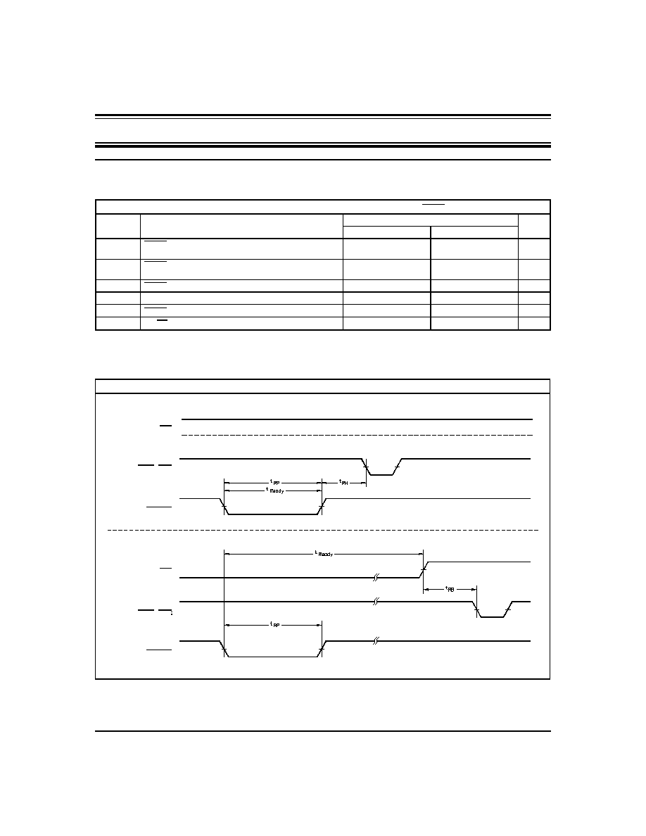
Figure 8: FLASH; RESET TIMING
Reset Timings Not during Embedded Algorithms
Reset Timings during Embedded Algorithms
RY/BY
FCS, OE
RESET
RY/BY
FCS, OE
RESET
FLASH: AC CHARACTERISTICS - Hardware Reset:
(RESET)
Symbol
Description
70ns
Units
Min.
Max.
t
Ready
RESET Pin Low (During Embedded Algorithms) to
Read Mode*
20
µ
s
t
Ready
RESET Pin Low (NOT During Embedded Algorithms)
to Read Mode*
500
ns
t
RP
RESET Pulse Width
500
ns
t
RH
Reset High Time Before Read*
50
ns
t
RPD
RESET Low to Standby Mode
20
µ
s
t
RB
RY/BY Recovery Time
0
ns
* Not 100% tested.
30A193-00
REV. C
20

Dense-Pac Microsystems, Inc.
DP3SZ128512X16NY5
ADVANCED INFORMATION
FLASH: AC CHARACTERISTICS - Word/Byte Configuration:
(BYTE)
Symbol
Description
70ns
Units
Min.
Max.
t
ELFL
/t
ELFH
FCS to BYTE Switching Low or High
5
ns
t
FLQZ
BYTE Switching Low to Output High-Z
25
ns
t
FHQV
BYTE Switching High to Output Active
70
ns
Figure 9: FLASH; BYTE TIMING FOR READ OPERATIONS
FCS
OE
BYTE
I/O0-I/O14
I/O15 / A-1
BYTE
I/O0-I/O14
I/O15 / A-1
BYTE Switch from Byte to Word Mode
BYTE Switch from Word to Byte Mode
Figure 10: FLASH; BYTE TIMING FOR WRITE OPERATIONS
FCS
WE
BYTE
30A193-00
REV. C
21

DP3SZ128512X16NY5
Dense-Pac Microsystems, Inc.
ADVANCED INFORMATION
FLASH: AC CHARACTERISTICS - Erase and Program Operations
Symbol
Description
70ns
Units
Min.
Typ.
Max.
t
WC
Write Cycle Time
1
70
ns
t
AS
Address Setup Time
0
ns
t
ASO
Address Setup Time to OE Low During Toggle Bit
Polling
45
ns
t
AH
Address Hold Time
45
ns
t
AHT
Address Hold Time from FCS or OE High During
Toggle Bit Polling
0
ns
t
DS
Data Setup Time
35
ns
t
DH
Data Hold Time
0
ns
t
OEPH
Output Enable High During Toggle Bit Polling
20
ns
t
GHWL
Read Recovery Time before Write
(OE High to WE Low)
0
ns
t
CS
FCS Setup Time
0
ns
t
CH
FCS Hold Time
0
ns
t
WP
Write Pulse Width
35
ns
t
WPH
Write Pulse Width High
30
ns
t
SR/W
Zero Latency between Read and Write Operations
0
ns
t
WHWH1
Programming Operation
1, 2
Byte
9
µ
s
Word
11
t
WHWH2
Sector Erase Operations
1, 2
0.7
sec
t
VCS
V
CC
Setup Time
50
µ
s
t
RB
Write Recovery Time from RY/BY
0
ns
t
BUSY
Program/Erase Valid to RY/BY Delay
90
ns
NOTES:
1. Not 100% tested.
2. See the "Erase and Programming Performance" section for more information.
30A193-00
REV. C
22

Dense-Pac Microsystems, Inc.
DP3SZ128512X16NY5
ADVANCED INFORMATION
Figure 11: FLASH; PROGRAM OPERATION TIMING
Figure 12: FLASH; CHIP/SECTOR OPERATION TIMINGS
ADDRESS
FCS
OE
WE
DATA
RY/BY
V
CC
NOTES:
1. PA = Program Address, PD = Program Data, D
OUT
is the true data at the Program Address.
2. Illustration shows device in Word Mode.
ADDRESS
FCS
OE
WE
DATA
RY/BY
V
CC
NOTES:
1. SA = Sector Address (for Sector Erase), VA = Valid Address for reading status data (see "Wr
ite Operation Status").
2. Illustration shows device in Word Mode.
30A193-00
REV. C
23

DP3SZ128512X16NY5
Dense-Pac Microsystems, Inc.
ADVANCED INFORMATION
Figure 13: FLASH; BACK-TO-BACK READ/WRITE CYCLE TIMING
Figure 14: FLASH; DATA POLLING TIMINGS (During Embedded Algorithms)
ADDRESS
FCS
OE
WE
DATA
ADDRESS
FCS
OE
WE
I/O7
I/O0-I/O6
RY/BY
NOTE:
VA = Valid Address. Illustration shows first status cycle after command sequence, last rea
d cycle, and array data read cycle.
30A193-00
REV. C
24

Dense-Pac Microsystems, Inc.
DP3SZ128512X16NY5
ADVANCED INFORMATION
Figure 15: FLASH; TOGGLE BIT TIMING (During Embedded Algorithms)
Figure 16: FLASH; CHIP/SECTOR OPERATION TIMINGS
ADDRESS
FCS
WE
OE
I/O6,I/O2
RY/BY
NOTES:
1. VA = Valid Address. Not required for I/O6.
2. Illustration shows first two status cycle after command sequence, last status read cycle,
and array data read cycle.
WE
I/O6
I/O2
NOTE:
I/O2 toggles only when read at an address within an erase-suspend sector. The system may use o
nly one OE or FCS to toggle I/O2 and I/O6.
30A193-00
REV. C
25

DP3SZ128512X16NY5
Dense-Pac Microsystems, Inc.
ADVANCED INFORMATION
FLASH: AC CHARACTERISTICS - Temporary Sector Unprotect
Symbol
Description
70ns
Units
Min.
Max.
t
VIDR
VID Rise and Fall Time
500
ns
t
RSP
RESET Setup Time for Temporary Sector Unprotect
4
µ
s
t
RRB
RESET Hold Time from RY/BY High for Temporary
Sector Unprotect
4
µ
s
Figure 18: FLASH; SECTOR PROTECT/UNPROTECT TIMING
Figure 17: FLASH; TEMPORARY SECTOR UNPROTECT TIMING
VID
VIH
ADDRESS
SA, A6, A1, A0
DATA
FCS
WE
OE
* For sector protect, A6 = 0, A1 = 1, A0 = . For sector unprotect, A6 = 1, A1 = 1, A0 = 0.
12.0V
RESET
0V or 3.0V
FCS
WE
RY/BY
30A193-00
REV. C
26

Dense-Pac Microsystems, Inc.
DP3SZ128512X16NY5
ADVANCED INFORMATION
FLASH: AC CHARACTERISTICS - Alternate RAMCS Controlled Erase/Program Operations
Symbol
Description
70ns
Units
Min.
Typ.
Max.
t
WC
Write Cycle Time
1
70
ns
t
AS
Address Setup Time
0
ns
t
AH
Address Hold Time
45
ns
t
DS
Data Setup Time
35
ns
t
DH
Data Hold Time
0
ns
t
GHEL
Read Recovery Time before Write
(OE High to WE Low)
0
ns
t
WS
WE Setup Time
0
ns
t
WH
WE Hold Time
0
ns
t
CP
FCS Pulse Width
35
ns
t
CPH
FCS Pulse Width High
30
ns
t
WHWH1
Programming Operation
1, 2
Byte
9
µ
s
Word
11
t
WHWH2
Sector Erase Operations
1, 2
0.7
sec
NOTES:
1. Not 100% tested.
2. See the "Erase and Programming Performance" section for more information.
Figure 19: ALTERNATE FCS CONTROLLED ERASE/PROGRAM OPERATION TIMING
ADDRESS
WE
OE
FCS
DATA
RESET
RY/BY
NOTES:
1. 555 for program, 2AA for erase.
2. PA for program, SA for sector erase, 555 for chip erase.
3. A0 for program, 55 for erase.
4. PD for program, 30 for sector erase, 10 for chip erase.
5. Figure indicates last two bus cycles of a program or erase
operation.
6. PA = Program Address, SA = Sector Address, PD =
Program Data, I/O7 = complement of the data written to
the device, D
OUT
= data written to the device.
7. Waveforms are for the word mode.
30A193-00
REV. C
27

DP3SZ128512X16NY5
Dense-Pac Microsystems, Inc.
ADVANCED INFORMATION
FLASH: AC CHARACTERISTICS - Erase and Program Performance
Comments
Description
70ns
Units
Min.
1
Max.
2
Excludes 00h
Programming Prior to Erasure
4
Sector Erase Time
0.7
15
sec
Chip Erase Time
14
sec
Excludes
System Level Overhead
5
Byte Program Time
9
300
µ
s
Word Program Time
11
360
µ
s
Chip Programming Time
3
Byte Mode
9
27
sec
Word Mode
5.8
17
NOTES:
1. Typical Program erase times assume the following conditions: +25
∞
C, 3.0V
V
CC
, 1,000,000 cycles. Additionally,
programming typically assume checkerboard pattern.
2. Under worst case conditions of +90
∞
C, V
CC
= 2.7V, 100,000 cycles.
3. The typical chip programming time is considerably less than the maximum chip programming time listed, since most bytes
program faster than the maximum program time listed.
4. In the pre-programming step of the Embedded Erase algorithm, all bytes are programmed to 00h before erasure.
5. System-level overhead is the time required to execute the two-bus-cycle or four-bus-cycle sequence for the program command.
See Table 3 for further information on command definitions.
6. The device has guaranteed erase and program cycle endurance of 1,000,000 cycles.
FLASH: Data Retention Characteristics
Parameter Description
Test Conditions
Min.
Unit
Minimum Pattern Data Retention Time
+150
∞
C
10
Years
+125
∞
C
20
Years
30A193-00
REV. C
28

Dense-Pac Microsystems, Inc.
DP3SZ128512X16NY5
ADVANCED INFORMATION
Dense-Pac Microsystems, Inc.
7321 Lincoln Way Garden Grove , California 92841-1431
(714) 898-0007 (800) 642-4477
(Outside CA)
FAX: (714) 897-1772 http://www.dense-pac.com
MECHANICAL DRAWING
ORDERING INFORMATION
30A193-00
REV. C
29