
16 Megabit FLASH EEPROM
DP5Z2MX8PAnY
PRELIMINARY
DESCRIPTION:
The DP5Z2MX8PAnY "SLCC" devices are a revolutionary new memory
subsystem using Dense-Pac Microsystems' ceramic Stackable Leadless Chip
Carriers (SLCC). Available unleaded, straight leaded, "J" leaded, gullwing
leaded packages, or mounted on a 50-pin PGA co-fired ceramic substrate.
The Device packs 16-Megabits of FLASH EEPROM in an area as small as
0.463 in2 while maintaining a total height as low as 0.171 inches.
The DP5Z2MX8PAnY is a 2 Meg x 8 FLASH EEPROM based memory module.
Each SLCC is hermetically sealed making the module suitable for commercial,
industrial and military applications.
By using SLCCs, the "Stack" family of modules offer a higher board density
of memory than available with conventional through-hole, surface mount or
hybrid techniques.
FEATURES:
∑
Organization: 2 Meg x 8
∑
Fast Access Times: 70*, 90, 120, 150ns (max.)
* V
DD
= 5.0V
±
5%
∑
Single 5.0 Volt Power Supply
∑
High-Density Symmetrically Blocked Architecture
- 32 Uniform Sectors of 64 Kbytes Each
∑
Extended Cycling Capability
- 100,000 Write/Erase Cycles per Sector
∑
Automated Erase and Program Cycles
- Command User Interface
- Status Register
∑
SRAM-Compatible Write Interface
∑
Hardware Data Protection Feature
- Erase / Write Lockout during Power Transitions
∑
Packages Available:
DP5Z2MX8PAY
48 - Pin SLCC
DP5Z2MX8PAIY
48 - Pin Straight Leaded SLCC
DP5Z2MX8PAHY
48 - Pin Gullwing Leaded SLCC
DP5Z2MX8PAJY
48 - Pin J Leaded SLCC
DP5Z2MX8PAA3
50 - Pin PGA Dense-SLCC
This document contains information on a product under consideration for
development at Dense-Pac Microsystems, Inc. Dense-Pac reserves the right
to
c
hange or discontinue information on this product without prior notice.
DP5Z2MX8PAH3
DP5Z2MX8PAY3
DP5Z2MX8PAI3
DP5Z2MX8PAJ3
DP5Z2MX8PAA3
30A161-A1
Rev. A
1
DP5Z2MX8PAn3
Dense-Pac Microsystems, Inc.
PRELIMINARY
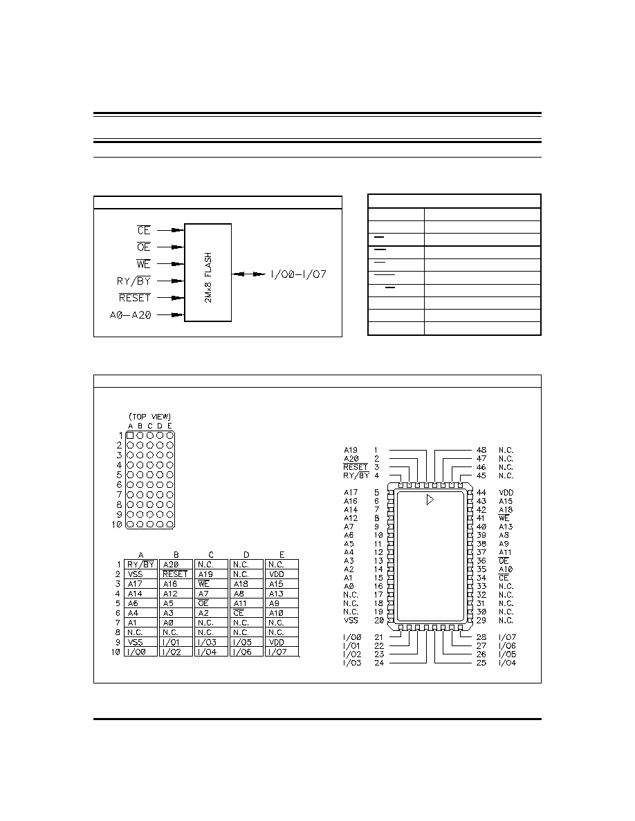
PIN NAMES
A0 - A20
Address
I/O0 - I/O7
Data Inputs/Outputs
CE
Chip Enable
WE
Write Enable
OE
Output Enable
RESET
Hardware reset Pin, Active Low
RY/BY
Ready/Busy Output
V
DD
Single Power (+5.0V)
V
SS
Ground
N.C.
No Connect
PIN-OUT DIAGRAM
FUNCTIONAL BLOCK DIAGRAM
50 - PIN PGA
DENSE-STACK
48 - PIN SLCC
48 - PIN STRAIGHT LEADED SLCC
48 - PIN GULLWING LEADED SLCC
48 - PIN J LEADED SLCC
48 - PIN PGA DENSE-SLCC
30A161-A1
Rev. A
2

Dense-Pac Microsystems, Inc.
DP5Z2MX8PAn3
PRELIMINARY
BUS OPERATION
This section describes the requirements and use of the device
bus operations, which are initiated through the internal
command register. The command register itself does not occupy
any addressable memory locations. The register is composed of
latches that store the commands, along with the address and data
information needed to execute the command. The contents of
the register serve as inputs to the internal state machine. The
state machine outputs dictate the function of the device. The
appropriate device bus operations table lists the inputs and
control levels required, and the resulting output. The following
subsections describe each of these operations in further detail.
Table 1. Device Bus Operation
Operation
CE
OE
WE
RESET
A0 - A20
I/O0 - I/O7
Read
L
L
H
H
A
IN
D
OUT
Write
L
H
L
H
A
IN
D
IN
CMOS Standby
V
DD
±
0.5V
X
X
V
DD
±
0.5V
X
HIGH-Z
TTL Standby
H
X
X
H
X
HIGH-Z
Output Disable
L
H
H
H
X
HIGH-Z
Hardware Reset
X
X
X
L
X
HIGH-Z
Temporary Sector Unprotect (See Note)
X
X
X
V
ID
A
IN
D
IN
Legend: L = Logic LOW = V
IL
H = Logic HIGH = V
IH
, V
ID
= 12.0
±
0.5V, X = Don't Care, D
IN
= Data In, D
OUT
= Data Out, A
IN
= Address In
Requirements for Reading Array Data
To read array data from the outputs, the system must drive the
CE and OE pins to V
IL
. CE is the power control and selects the
device. OE is the output control and gates array data to the output
pins. WE should remain at V
IH
.
The internal state machine is set for reading array data upon
device power-up, or after a hardware reset. This ensures that no
spurious alteration of the memory content occurs during the
power transition. No command is necessary in this mode to
obtain array data. Standard microprocessor read cycles that
assert valid addresses on the device address inputs produce valid
data on the device data outputs. The device remains enabled for
read access until the command register contents are altered.
See "Reading Array Data" for more information. Refer to the AC
Read Operations table for timing specifications and to the Read
Operations Timings diagram for the timing waveforms. I
CC1
in
the DC Characteristics table represents the active current
specification for reading array data.
Writing Commands/Command Sequences
To write a command or command sequence (which includes
programming data to the device and erasing sectors of memory),
the system must drive WE and CE to V
IL
, and OE to V
IH
.
An erase operation can erase one sector, multiple sectors, or the
entire device. The Sector Address Tables indicate the address
space that each sector occupies. A "Sector Address" consists of
the address bits required to uniquely select a sector. See the
"Command Definitions" section for details on erasing a sector or
the entire chip, or suspending/resuming the erase operation.
After the system writes the autoselect command sequence, the
device enters the autoselect mode. The system can then read
autoselect codes from the internal register (which is separate
from the memory array) on I/O7-I/O0. Standard read cycle
timings apply in this mode. Refer to the "Autoselect Mode" and
"Autoselect Command Sequence" sections for more information.
I
CC2
in the DC Characteristics table represents the active current
specification for the write mode. The "AC Characteristics"
section contains timing specification tables and timing diagrams
for write operations.
Program and Erase Operation Status
During an erase or program operation, the system may check the
status of the operation by reading the status bits on I/O7-I/O0.
Standard read cycle timings and I
CC
read specifications apply.
Refer to "Write Operation Status" for more information, and to
each AC Characteristics section for timing diagrams.
30A161-A1
Rev. A
3

DP5Z2MX8PAn3
Dense-Pac Microsystems, Inc.
PRELIMINARY
Standby Mode
When the system is not reading or writing to the device, it can
place the device in the standby mode. In this mode, current
consumption is greatly reduced, and the outputs are placed in
the high impedance state, independent of the OE input.
The device enters the CMOS standby mode when CE and RESET
pins are both held at V
DD
0.5 V. (Note that this is a more
restricted voltage range than V
IH
.) The device enters the TTL
standby mode when CE and RESET pins are both held at V
IH
.
The device requires standard access time (t
CE
) for read access
when the device is in either of these standby modes, before it is
ready to read data.
The device also enters the standby mode when the RESET pin is
driven low. Refer to the next section, "RESET: Hardware Reset
Pin".
If the device is deselected during erasure or programming, the
device draws active current until the operation is completed.
In the DC Characteristics tables, I
SB1
and I
SB2
represent the
standby current specification.
RESET: Hardware Reset Pin
The RESET pin provides a hardware method of resetting the
device to reading array data. When the system drives the RESET
pin low for at least a period of t
RP
, the device immediately
terminates any operation in progress, tristates all data output
pins, and ignores all read/write attempts for the duration of the
RESET pulse. The device also resets the internal state machine
to reading array data. The operation that was interrupted should
be reinitiated once the device is ready to accept another
command sequence, to ensure data integrity.
Current is reduced for the duration of the RESET pulse. When
RESET is held at V
IL
, the device enters the TTL standby mode; if
RESET is held at V
SS
±
0.5V, the device enters the CMOS standby
mode.
The RESET pin may be tied to the system reset circuitry. A system
reset would thus also reset the Flash memory, enabling the system
to read the boot-up firmware from the Flash memory.
If RESET is asserted during a program or erase operation, the
RY/BY pin remains a "0" (busy) until the internal reset operation
is complete, which requires a time of t
READY
(during Embedded
Algorithms). The system can thus monitor RY/BY to determine
whether the reset operation is complete. If RESET is asserted
when a program or erase operation is not executing (RY/BY pin
is "1"), the reset operation is completed within a time of t
READY
(not during Embedded Algorithms). The system can read data
t
RH
after the RESET pin returns to V
IH
.
Refer to the AC Characteristics tables for RESET parameters and
timing diagram.
Output Disable Mode
When the OE input is at V
IH
, output from the device is disabled.
The output pins are placed in the high impedance state.
Autoselect Mode
The autoselect mode provides manufacturer and device
identification through identifier codes output on I/O7-I/O0. This
mode is primarily intended for programming equipment to
automatically match a device to be programmed with its
corresponding programming algorithm. However, the autoselect
codes can also be accessed in-system through the command
register.
When using programming equipment, the autoselect mode
requires V
ID
(11.5V to 12.5V) on address pin A9. Address pins
A6, A1, and A0 must be as shown in Table 2, Autoselect Codes
(High Voltage Method). The "Command Definitions", table 4,
shows the remaining address bits that are don't care. When all
necessary bits have been set as required, the programming
equipment may then read the corresponding identifier code on
I/O7-I/O0.
To access the autoselect codes in-system, the host system can
issue the autoselect command via the command register, as
shown in the "Command Definitions" table. This method does
not require V
ID
. See Command Definitions for details on using
the autoselect mode.
Table 2. Auto Select Codes
(High Voltage Method)
Description
CE
OE
WE A20-A18 A17-A10 A9
A8-A7
A6
A5-A2
A1
A0
I/O7-I/O0
Manufacture ID
L
L
H
X
X
V
ID
X
V
IL
X
V
IL
V
IL
01h
Device ID
L
L
H
X
X
V
ID
X
V
IL
X
V
IL
V
IH
ADh
L = Logic Low = V
IL
, H = Logic High = V
IH
, SA = Sector Address, X = Don't Care.
30A161-A1
Rev. A
4

Dense-Pac Microsystems, Inc.
DP5Z2MX8PAn3
PRELIMINARY
Table 3: SECTOR ADDRESS
Sector
A20
A19
A18
A17
A16
Address Range
SA0
0
0
0
0
0
000000h-00FFFFh
SA1
0
0
0
0
1
010000h-01FFFFh
SA2
0
0
0
1
0
020000h-02FFFFh
SA3
0
0
0
1
1
030000h-03FFFFh
SA4
0
0
1
0
0
040000h-04FFFFh
SA5
0
0
1
0
1
050000h-05FFFFh
SA6
0
0
1
1
0
060000h-06FFFFh
SA7
0
0
1
1
1
070000h-07FFFFh
SA8
0
1
0
0
0
080000h-08FFFFh
SA9
0
1
0
0
1
090000h-09FFFFh
SA10
0
1
0
1
0
0A0000h-0AFFFFh
SA11
0
1
0
1
1
0B0000h-0BFFFFh
SA12
0
1
1
0
0
0C0000h-0CFFFFh
SA13
0
1
1
0
1
0D0000h-0DFFFFh
SA14
0
1
1
1
0
0E0000h-0EFFFFh
SA15
0
1
1
1
1
0F0000h-0FFFFFh
SA16
1
0
0
0
0
100000h-10FFFFh
SA17
1
0
0
0
1
110000h-11FFFFh
SA18
1
0
0
1
0
120000h-12FFFFh
SA19
1
0
0
1
1
130000h-13FFFFh
SA20
1
0
1
0
0
140000h-14FFFFh
SA21
1
0
1
0
1
150000h-15FFFFh
SA22
1
0
1
1
0
160000h-16FFFFh
SA23
1
0
1
1
1
170000h-17FFFFh
SA24
1
1
0
0
0
180000h-18FFFFh
SA25
1
1
0
0
1
190000h-19FFFFh
SA26
1
1
0
1
0
1A0000h-1AFFFFh
SA27
1
1
0
1
1
1B0000h-1BFFFFh
SA28
1
1
1
0
0
1C0000h-1CFFFFh
SA29
1
1
1
0
1
1D0000h-1DFFFFh
SA30
1
1
1
1
0
1E0000h-1EFFFFh
SA31
1
1
1
1
1
1F0000h-1FFFFFh
NOTE: All sectors are 64 Kbytes in size.
30A161-A1
Rev. A
5

DP5Z2MX8PAn3
Dense-Pac Microsystems, Inc.
PRELIMINARY
Hardware Data Protection
The command sequence requirement of unlock cycles for
programming or erasing provides data protection against
inadvertent writes (refer to Table 3, Command Definitions). In
addition, the following hardware data protection measures
prevent accidental erasure or programming, which might
otherwise be caused by spurious system level signals during V
DD
power-up and power-down transitions, or from system noise.
Low V
DD
Write Inhibit
When V
DD
is less than V
LKO
, the device does not accept any write
cycles. This protects data during V
DD
power-up and power-
down. The command register and all internal program/erase
circuits are disabled, and the device resets. Subsequent writes
are ignored until V
DD
is greater than V
LKO
. The system must
provide the proper signals to the control pins to prevent
unintentional writes when V
DD
is greater than V
LKO
.
Write Pulse "Glitch" Protection
Noise pulses of less than 5ns (typical) on OE, CE or WE do not
initiate a write cycle.
Logical Inhibit
Write cycles are inhibited by holding any one of OE = V
IL
, CE
= V
IH
or WE = V
IH
. To initiate a write cycle, CE and WE must
be a logical zero while OE is a logical one.
Power-Up Write Inhibit
If WE = CE = V
IL
and OE = V
IH
during power up, the device
does not accept commands on the rising edge of WE. The internal
state machine is automatically reset to reading array data on
power-up.
COMMAND DEFINITIONS
Writing specific address and data commands or sequences into
the command register initiates device operations. The Command
Definitions table defines the valid register command sequences.
Writing incorrect address and data values or writing them in
the improper sequence resets the device to reading array data.
All addresses are latched on the falling edge of WE or CE,
whichever happens later. All data is latched on the rising edge of
WE or CE, whichever happens first. Refer to the appropriate
timing diagrams in the "AC Characteristics" section.
Reading Array Data
The device is automatically set to reading array data after device
power-up. No commands are required to retrieve data. The
device is also ready to read array data after completing an
Embedded Program or Embedded Erase algorithm.
After the device accepts an Erase Suspend command, the device
enters the Erase Suspend mode. The system can read array data
using the standard read timings, except that if it reads at an
address within erase-suspended sectors, the device outputs
status data. After completing a programming operation in the
Erase Suspend mode, the system may once again read array data
with the same exception. See "Erase Suspend/Erase Resume
Commands" for more information on this mode.
The system must issue the reset command to re-enable the
device for reading array data if I/O5 goes high, or while in the
autoselect mode. See the "Reset Command" section, next.
See also "Requirements for Reading Array Data" in the "Device
Bus Operations" section for more information. The Read
Operations table provides the read parameters, and Read
Operation Timings diagram shows the timing diagram.
Reset Command
Writing the reset command to the device resets the device to
reading array data. Address bits are don't care for this command.
The reset command may be written between the sequence
cycles in an erase command sequence before erasing begins. This
resets the device to reading array data. Once erasure begins,
however, the device ignores reset commands until the operation
is complete.
The reset command may be written between the sequence
cycles in a program command sequence before programming
begins. This resets the device to reading array data (also applies
to programming in Erase Suspend mode). Once programming
begins, however, the device ignores reset commands until the
operation is complete.
The reset command may be written between the sequence
cycles in an autoselect command sequence. Once in the
autoselect mode, the reset command must be written to return
to reading array data (also applies to autoselect during Erase
Suspend).
If I/O5 goes high during a program or erase operation, writing
the reset command returns the device to reading array data (also
applies during Erase Suspend).
Autoselect Command Sequence
The autoselect command sequence allows the host system to
access the manufacturer and devices codes, and determine
whether or not a sector is protected. The Command Definitions
table shows the address and data requirements. This method is
an alternative to that shown in Table 2, Autoselect Codes (High
Voltage Method), which is intended for PROM programmers and
requires V
ID
on address bit A9.
The autoselect command sequence is initiated by writing two
unlock cycles, followed by the autoselect command. The device
then enters the autoselect mode, and the system may read at any
address any number of times, without initiating another
command sequence.
30A161-A1
Rev. A
6

Dense-Pac Microsystems, Inc.
DP5Z2MX8PAn3
PRELIMINARY
A read cycle at address XX00h retrieves the manufacturer code.
A read cycle at address XX01h returns the device code. A read
cycle containing a sector address (SA) and the address 02h in
returns 01h if that sector is protected, or 00h if it is unprotected.
Refer to the Sector Address tables for valid sector addresses.
The system must write the reset command to exit the autoselect
mode and return to reading array data.
Byte Program Command Sequence
Programming is a four-bus-cycle operation. The program
command sequence is initiated by writing two unlock write
cycles, followed by the program set-up command. The program
address and data are written next, which in turn initiate the
Embedded Program algorithm. The system is not required to
provide further controls or timings. The device automatically
provides internally generated program pulses and verify the
programmed cell margin. The Command Definitions table
shows the address and data requirements for the byte program
command sequence.
When the Embedded Program algorithm is complete, the device
then returns to reading array data and addresses are no longer
latched. The system can determine the status of the program
operation by using I/O7, I/O6, or RY/BY. See "Write Operation
Status ` for information on these status bits.
Any commands written to the device during the Embedded
Program Algorithm are ignored. Note that a hardware reset
immediately terminates the programming operation. The
program command sequence should be reinitiated once the
device has reset to reading array data, to ensure data integrity.
Programming is allowed in any sequence and across sector
boundaries. A bit cannot be programmed from a "0" back to
a "1". Attempting to do so may halt the operation and set I/O5
to 1, or cause the Data Polling algorithm to indicate the operation
was successful. However, a succeeding read will show that the
data is still "0". Only erase operations can convert a "0" to a "1".
Chip Erase Command Sequence
Chip erase is a six-bus-cycle operation. The chip erase command
sequence is initiated by writing two unlock cycles, followed by
a set-up command. Two additional unlock write cycles are then
followed by the chip erase command, which in turn invokes the
Embedded Erase algorithm. The device does not require the
system to preprogram prior to erase. The Embedded Erase
algorithm automatically preprograms and verifies the entire
memory for an all zero data pattern prior to electrical erase. The
system is not required to provide any controls or timings during
these operations. The Command Definitions table shows the
address and data requirements for the chip erase command
sequence.
Any commands written to the chip during the Embedded Erase
algorithm are ignored. Note that a hardware reset during the
chip erase operation immediately terminates the operation. The
Chip Erase command sequence should be reinitiated once the
device has returned to reading array data, to ensure data integrity.
The system can determine the status of the erase operation by
using I/O7, I/O6, I/O2, or RY/BY. See "Write Operation Status"
for information on these status bits. When the Embedded Erase
algorithm is complete, the device returns to reading array data
and addresses are no longer latched.
Figure 2 illustrates the algorithm for the erase operation. See the
Erase/Program Operations tables in "AC Characteristics" for
parameters, and to the Chip/Sector Erase Operation Timings for
timing waveforms.
Sector Erase Command Sequence
Sector erase is a six bus cycle operation. The sector erase
command sequence is initiated by writing two unlock cycles,
followed by a set-up command. Two additional unlock write
cycles are then followed by the address of the sector to be erased,
and the sector erase command. The Command Definitions table
shows the address and data requirements for the sector erase
command sequence.
The device does not require the system to preprogram the
memory prior to erase. The Embedded Erase algorithm
automatically programs and verifies the sector for an all zero data
pattern prior to electrical erase. The system is not required to
provide any controls or timings during these operations.
After the command sequence is written, a sector erase time-out
of 50
µ
s begins. During the time-out period, additional sector
addresses and sector erase commands may be written. Loading
the sector erase buffer may be done in any sequence, and the
Figure 1. Program Operation
Note: See the table 4 for appropriate Command Definitions.
30A161-A1
Rev. A
7

DP5Z2MX8PAn3
Dense-Pac Microsystems, Inc.
PRELIMINARY
number of sectors may be from one sector to all sectors. The
time between these additional cycles must be less than 50
µ
s,
otherwise the last address and command might not be accepted,
and erasure may begin. It is recommended that processor
interrupts be disabled during this time to ensure all commands
are accepted. The interrupts can be re-enabled after the last
Sector Erase command is written. If the time between additional
sector erase commands can be assumed to be less than 50s, the
system need not monitor I/O3. Any command other than
Sector Erase or Erase Suspend during the time-out period
resets the device to reading array data. The system must rewrite
the command sequence and any additional sector addresses and
commands.
The system can monitor I/O3 to determine if the sector erase
timer has timed out. (See the "I/O3: Sector Erase Timer"
section.) The time-out begins from the rising edge of the final WE
pulse in the command sequence.
Once the sector erase operation has begun, only the Erase
Suspend command is valid. All other commands are ignored.
Note that a hardware reset during the sector erase operation
immediately terminates the operation. The Sector Erase
command sequence should be reinitiated once the device has
returned to reading array data, to ensure data integrity.
When the Embedded Erase algorithm is complete, the device
returns to reading array data and addresses are no longer latched.
The system can determine the status of the erase operation by
using I/O7, I/O6, I/O2, or RY/BY. Refer to Write Operation Status
for information on these status bits.
Figure 2 illustrates the algorithm for the erase operation. Refer
to the Erase/Progra m Operations tables in the "AC
Characteristics" section for parameters, and to the Sector Erase
Operations Timing diagram for timing waveforms.
Erase Suspend/Erase Resume Commands
The Erase Suspend command allows the system to interrupt a
sector erase operation and then read data from, or program data
to, any sector not selected for erasure. This command is valid
only during the sector erase operation, including the 50
µ
s
time-out period during the sector erase command sequence. The
Erase Suspend command is ignored if written during the chip
erase operation or Embedded Program algorithm. Writing the
Erase Suspend command during the Sector Erase time-out
immediately terminates the time-out period and suspends the
erase operation. Addresses are "don't-cares" when writing the
Erase Suspend command.
When the Erase Suspend command is written during a sector
erase operation, the device requires a maximum of 20
µ
s to
suspend the erase operation. However, when the Erase Suspend
command is written during the sector erase time-out, the device
immediately terminates the time-out period and suspends the
erase operation.
After the erase operation has been suspended, the system can
read array data from or program data to any sector not selected
for erasure. (The device "Erase Suspends" all sectors selected for
erasure.) Normal read and write timings and command
definitions apply. Re ading at a ny a ddress within
erase-suspended sectors produces status data on I/O7-I/O0. The
system can use I/O7, or I/O6 and I/O2 together, to determine if
a sector is actively erasing or is erase-suspended. See "Write
Operation Status" for information on these status bits.
After an erase-suspended program operation is complete, the
system can once again read array data within non-suspended
sectors. The system can determine the status of the program
operation using the I/O7 or I/O6 status bits, just as in the standard
program operation. See Write Operation Status for more
information. The system may also write the autoselect command
sequence when the device is in the Erase Suspend mode. The
device allows reading autoselect codes even at addresses within
erasing sectors, since the codes are not stored in the memory
array. When the device exits the autoselect mode, the device
reverts to the Erase Suspend mode, and is ready for another valid
operation. See "Autoselect Command Sequence" for more
information.
The system must write the Erase Resume command (address bits
are don't care) to exit the erase suspend mode and continue the
sector erase operation. Further writes of the Resume command
are ignored. Another Erase Suspend command can be written
after the device has resumed erasing.
Figure 2. Erase Operation
Notes:
1. See the appropriate Command Definitions table for erase command
sequence.
2. See "I/O3: Sector Erase Timer" for more information.
30A161-A1
Rev. A
8
Dense-Pac Microsystems, Inc.
DP5Z2MX8PAn3
PRELIMINARY
Command Definition Notes:
1. See Table 1 for description of bus operations.
2. All values are in hexadecimal.
3. Except when reading array or autoselect data, all bus cycles are write
operations.
4. Address bits A20 - A11 are don't cares for unlock and command
cycles, unless SA or PA required.
5. No unlock or command cycles required when reading array data.
6. The Reset command is required to return to reading array data when
device is in the autoselect mode, or if I/O5 goes high (while the device
is providing status data).
7. The fourth cycle of the autoselect command sequence is a read cycle.
8. The data is 00h for an unprotected sector group and 01h for a
protected sector group. See "Autoselect Command Sequence" for
more information.
9. The system may read and program in non-erasing sectors, or enter the
autoselect mode, when in the Erase Suspend mode. The Erase
Suspend command is valid only during a sector erase operation.
10. The Erase Resume command is valid only during the Erase Suspend
mode.
Table 4: Command Definitions
Command Sequence
1
Bus Cycles
2, 3 & 4
First
Second
Third
Forth
Fifth
Sixth
Address Data Address Data Address Data Address Data Address Data Address Data
Read
5
1
RA
F0
-
-
-
-
-
-
-
-
-
-
Reset
6
1
XXX
F0
-
-
-
-
-
-
-
-
-
-
Autoselect
7
Manufacturer ID
4
555
AA
2AA
55
555
90
X00
01
-
-
-
-
Device ID
4
555
AA
2AA
55
555
90
X01
AD
-
-
-
-
Program
4
555
AA
2AA
55
555
A0
PA
PD
-
-
-
-
Chip Erase
6
555
AA
2AA
55
555
80
555
AA
2AA
55
555
10
Sector Erase
6
555
AA
2AA
55
555
8
555
AA
2AA
55
SA
30
Erase Suspend
9
1
XXX
B0
-
-
-
-
-
-
-
-
-
-
Ease Resume
10
1
XXX
30
-
-
-
-
-
-
-
-
-
-
Legend:
X
= Don't Care
RA
= Address of the memory location to be read.
RD
= Data read from location RA during read operation.
PA
= Address of the memory location to be programmed.
Addresses latch on the falling edge of the WE or CE pulse, whichever happens later.
PD
= Data to be programmed at location PA. Data latches on the rising edge of WE or CE pulse, whichever happens first.
SA
= Address of the sector to be verified (in autoselect mode) or erased.
Address bits A20 - A16 select a unique sector.
SGA = Address of the sector group to be verified. Address bits A20 - A18 select a unique sector group.
30A161-A1
Rev. A
9

DP5Z2MX8PAn3
Dense-Pac Microsystems, Inc.
PRELIMINARY
WRITE OPERATION STATUS
The device provides several bits to determine the status of a write operation: I/O2, I/O3, I/O5, I/O6, I/O7, and RY/BY. Table 5 and
the following subsections describe the functions of these bits. I/O7, RY/BY, and I/O6 each offer a method for determining whether
a program or erase operation is complete or in progress. These three bits are discussed first.
I/O7: Data Polling
The Data Polling bit, I/O7, indicates to the host system whether
an Embedded Algorithm is in progress or completed, or whether
the device is in Erase Suspend. Data Polling is valid after the rising
edge of the final WE pulse in the program or erase command
sequence.
During the Embedded Program algorithm, the device outputs on
I/O7 the complement of the datum programmed to I/O7. This
I/O7 status also applies to programming during Erase Suspend.
When the Embedded Program algorithm is complete, the device
outputs the datum programmed to I/O7. The system must
provide the program address to read valid status information on
I/O7. If a program address falls within a protected sector, Data
Polling on I/O7 is active for approximately 2
µ
s, then the device
returns to reading array data.
During the Embedded Erase algorithm, Data Polling produces a
"0" on I/O7. When the Embedded Erase algorithm is complete,
or if the device enters the Erase Suspend mode, Data Polling
produces a "1" on I/O7. This is analogous to the
complement/true datum output described for the Embedded
Program algorithm: the erase function changes all the bits in a
sector to "1"; prior to this, the device outputs the complement,
or "0". The system must provide an address within any of the
sectors selected for erasure to read valid status information on
I/O7.
After an erase command sequence is written, if all sectors
selected for erasing are protected, Data Polling on I/O7 is active
for approximately 100
µ
s, then the device returns to reading array
data. If not all selected sectors are protected, the Embedded
Erase algorithm erases the unprotected sectors, and ignores the
selected sectors that are protected.
When the system detects I/O7 has changed from the
complement to true data, it can read valid data at I/O7-I/O0 on
the following read cycles. This is because I/O7 may change
asynchronously with I/O0 - I/O6 while Output Enable (OE) is
asserted low. The Data Polling Timings (During Embedded
Algorithms) in the "AC Characteristics" section illustrates this.
Table 5 shows the outputs for Data Polling on I/O7. Figure 3
shows the Data Polling algorithm.
RY/BY: Ready/Busy
The RY/BY is a dedicated, open-drain output pin that indicates
whether an Embedded Algorithm is in progress or complete. The
RY/BY status is valid after the rising edge of the final WE pulse in
the command sequence. Since RY/BY is an open- drain output,
several RY/BY pins can be tied together in parallel with a pull-up
resistor to V
DD
.
If the output is low (Busy), the device is actively erasing or
programming. (This includes programming in the Erase Suspend
mode.) If the output is high (Ready), the device is ready to read
array data (including during the Erase Suspend mode), or is in
the standby mode.
Table 6 shows the outputs for RY/BY. The timing diagrams for
read, reset, program, and erase shows the relationship of RY/BY
to other signals.
Figure 3. Data Polling Algorithm
Notes:
1. VA = Valid address for programming. During a sector erase operation,
a valid address is an address within any sector selected for erasure.
During chip erase, a valid address is any non-protected sector address.
2. I/O7 should be rechecked even if I/O5 = "1" because I/O7 may change
simultaneously with I/O5.
30A161-A1
Rev. A
10

Dense-Pac Microsystems, Inc.
DP5Z2MX8PAn3
PRELIMINARY
I/O6: Toggle Bit I
Toggle Bit I on I/O6 indicates whether an Embedded Program or
Erase algorithm is in progress or complete, or whether the device
has entered the Erase Suspend mode. Toggle Bit I may be read
at any address, and is valid after the rising edge of the final WE
pulse in the command sequence (prior to the program or erase
operation), and during the sector erase time-out.
During an Embedded Program or Erase algorithm operation,
successive read cycles to any address cause I/O6 to toggle. (The
system may use either OE or CE to control the read cycles.) When
the operation is complete, I/O6 stops toggling.
After an erase command sequence is written, if all sectors
selected for erasing are protected, I/O6 toggles for approximately
100
µ
s, then returns to reading array data. If not all selected
sectors are protected, the Embedded Erase algorithm erases the
unprotected sectors, and ignores the selected sectors that are
protected.
The system can use I/O6 and I/O2 together to determine whether
a sector is actively erasing or is erase-suspended. When the
device is actively erasing (that is, the Embedded Erase algorithm
is in progress), I/O6 toggles. When the device enters the Erase
Suspend mode, I/O6 stops toggling. However, the system must
also use I/O2 to determine which sectors are erasing or
erase-suspended. Alternatively, the system can use I/O7 (see the
subsection on "I/O7: Data Polling").
If a program address falls within a protected sector, I/O6 toggles
for approximately 2
µ
s after the program command sequence is
written, then returns to reading array data.
I/O6 also toggles during the erase-suspend-program mode, and
stops toggling once the Embedded Program algorithm is
complete.
The Write Operation Status table shows the outputs for Toggle
Bit I on I/O6. Refer to Figure 4 for the toggle bit algorithm, and
to the "Toggle Bit Timings" in the AC Characteristics section for
the timing diagram. The I/O2 vs. I/O6 figure shows the
differences between I/O2 and I/O6 in graphical form. See also
the subsection on "I/O2: Toggle Bit II".
I/O2: Toggle Bit II
The Toggle Bit II on I/O2, when used with I/O6, indicates whether
a particular sector is actively erasing (that is, the Embedded Erase
algorithm is in progress), or whether that sector is
erase-suspended. Toggle Bit II is valid after the rising edge of the
final WE pulse in the command sequence.
I/O2 toggles when the system reads at addresses within those
sectors that have been selected for erasure. (The system may
use either OE or CE to control the read cycles.) But I/O2 cannot
distinguish whether the sector is actively erasing or is erase-
suspended. I/O6, by comparison, indicates whether the device
is actively erasing, or is in Erase Suspend, but cannot distinguish
which sectors are selected for erasure. Thus, both status bits are
required for sector and mode information. Refer to Table 6 to
compare outputs for I/O2 and I/O6.
Figure 4 shows the toggle bit algorithm in flowchart form, and
the section "I/O2: Toggle Bit II" explains the algorithm. See also
the "I/O6: Toggle Bit I" subsection. Refer to the Toggle Bit
Timings figure for the toggle bit timing diagram. The I/O2 vs. I/O6
figure shows the differences between I/O2 and I/O6 in graphical
form.
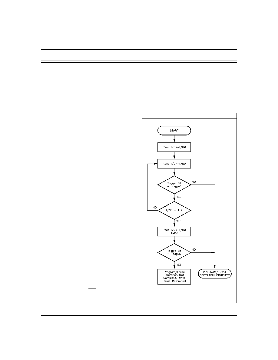
Reading Toggle Bits I/O6-I/O2
Refer to Figure 4 for the following discussion. Whenever the
system initially begins reading toggle bit status, it must read I/O7-
I/O0 at least twice in a row to determine whether a toggle bit is
Table 5. Write Operation Status
Operation
I/O7
1,3
I/O6
3
I/O5
2,3
I/O3
3
I/O2
3
RY/BY
Standard
Mode
Embedded Program Algorithm
I/O7
Toggle
0
N/A
No Toggle
0
Embedded Erase Algorithm
0
Toggle
0
1
Toggle
0
Erase
Suspend
Mode
Read within Erase
Suspended Sector
1
No Toggle
0
N/A
Toggle
1
Read within Non-Erase
Suspended Sector
Data
Data
Data
Data
Data
1
Erase-Suspend-Program
I/O7
Toggle
0
N/A
N/A
0
Notes:
1. I/O7 and I/O2 require a valid address when reading status
information. Refer to the appropriate subsection for further details.
2. I/O5 switches to 1 when an Embedded Program or Embedded Erase
operation has exceeded the maximum timing limits. See I/O5:
Exceeded Timing Limits for more information.
3. Data Polling Bits = I/O7, I/O15
Toggle Bits I = I/O6, I/O14
Exceeding Timing Limits Bits = I/O5, I/O13
Sector Erase Timer Bits = I/O3, I/O11
Toggle Bits II = I/O2, I/O10
30A161-A1
Rev. A
11
DP5Z2MX8PAn3
Dense-Pac Microsystems, Inc.
PRELIMINARY
toggling. Typically, a system would note and store the value of
the toggle bit after the first read. After the second read, the
system would compare the new value of the toggle bit with the
first. If the toggle bit is not toggling, the device has completed
the program or erase operation. The system can read array data
on I/O7- I/O0 on the following read cycle.
However, if after the initial two read cycles, the system
determines that the toggle bit is still toggling, the system also
should note whether the value of I/O5 is high (see the section on
I/O5). If it is, the system should then determine again whether
the toggle bit is toggling, since the toggle bit may have stopped
toggling just as I/O5 went high. If the toggle bit is no longer
toggling, the device has successfully completed the program or
erase operation. If it is still toggling, the device did not complete
the operation successfully, and the system must write the reset
command to return to reading array data.
The remaining scenario is that the system initially determines that
the toggle bit is toggling and I/O5 has not gone high. The system
may continue to monitor the toggle bit and I/O5 through
successive read cycles, determining the status as described in the
previous paragraph. Alternatively, it may choose to perform
other system tasks. In this case, the system must start at the
beginning of the algorithm when it returns to determine the status
of the operation (top of Figure 4).
I/O5: Exceeded Timing Limits
I/O5 indicates whether the program or erase time has exceeded
a specified internal pulse count limit. Under these conditions
I/O5 produces a "1". This is a failure condition that indicates the
program or erase cycle was not successfully completed.
The I/O5 failure condition may appear if the system tries to
program a "1" to a location that is previously programmed to 0.
Only an erase operation can change a "0" back to a "1". Under
this condition, the device halts the operation, and when the
operation has exceeded the timing limits, I/O5 produces a "1".
Under both these conditions, the system must issue the reset
command to return the device to reading array data.
I/O3: Sector Erase Timer
After writing a sector erase command sequence, the system may
read I/O3 to determine whether or not an erase operation has
begun. (The sector erase timer does not apply to the chip erase
command.) If additional sectors are selected for erasure, the
entire time-out also applies after each additional sector erase
command. When the time-out is complete, I/O3 switches from
"0" to "1". The system may ignore I/O3 if the system can
guarantee that the time between additional sector erase
commands will always be less than 50
µ
s. See also the Sector
Erase Command Sequence section.
After the sector erase command sequence is written, the system
should read the status on I/O7 (Data Polling) or I/O6 (Toggle Bit
I) to ensure the device has accepted the command sequence,
and then read I/O3. If I/O3 is "1", the internally controlled erase
cycle has begun; all further commands (other than Erase
Suspend) are ignored until the erase operation is complete. If
I/O3 is "0", the device will accept additional sector erase
commands. To ensure the command has been accepted, the
system software should check the status of I/O3 prior to and
following each subsequent sector erase command. If I/O3 is high
on the second status check, the last command might not have
been accepted. Table 5 shows the outputs for I/O3.
Figure 4. Toggle Bit Algorithm
Notes:
1. Read toggle bit twice to determine whether or not it is toggling. See text.
2. Recheck toggle bit because it may stop toggling as I/O5 changes to 1.
See text.
30A161-A1
Rev. A
12

Dense-Pac Microsystems, Inc.
DP5Z2MX8PAn3
PRELIMINARY
RECOMMENDED OPERATING RANGE
1
Symbol
Characteristic
Min. Typ.
Max.
Unit
V
DD
Supply Voltage
4.5
5.0
5.5
V
V
IH
Input HIGH Voltage
2.2
V
DD
+0.5
V
V
IL
Input LOW Voltage -0.5
2
0.8
V
T
A
Operating
Temperature
C
0
+25
+70
∫
C
I
-40
+25
+85
M/B -55
+25
+125
CAPACITANCE
6
:
T
A
= 25
∫
C, F = 1.0MHz
Symbol
Parameter
Max. Unit Condition
C
ADR
Address Input
10
pF
V
IN
= 0V
C
CE
Chip Enable
12
C
WE
Write Enable
12
C
OE
Output Enable
12
C
I/O
Data Input/Output
15
ABSOLUTE MAXIMUM RATING
Symbol
Parameter
Max.
Unit
T
STC
Storage Temperature
-65 to +150
∫
C
T
BIAS
Temperature Under Bias
-55 to +150
∫
C
T
OP
Operating Temperature
-55 to +150
∞
C
I
OUT
Output Short Circuit
Current
200
4
mA
V
DD
Supply Voltage
2
-0.5 to +7.0
3
V
V
I/O
Input/Output Voltage
A9, OE, RESET
3
-0.5 to +12.5
V
Input Voltage
All Other Pins
2
-0.5 to +7.0
DC OUTPUT CHARACTERISTICS
Symbol
Parameter
Condition Min. Max. Unit
V
OH
HIGH Voltage
I
OH
= 2.5mA
2.4
V
V
OL
LOW Voltage
I
OL
= 12mA
0.45
V
DC OPERATING CHARACTERISTICS:
Over Operating Ranges
Symbol
Characteristics
Test Condition
Min.
Typ.
Max.
Unit
I
LI
Input Load Current
V
IN
= V
SS
to V
DD
, V
DD
= V
DD
Max.
±
1.0
µ
A
I
LIT
A9 Input Load Current
V
DD
= V
DD
Max., A9 = 12.5V
50
µ
A
I
OUT
Output Leakage Current
V
OUT
=V
SS
to V
DD
, V
DD
= V
DD
Max.
±
1.0
µ
A
I
CC1
V
DD
Read Current
7
CE = V
IL
, OE = V
IH
25
40
mA
I
CC2
V
DD
Write Current
6, 8
CE = V
IL
, CE = V
IH
40
60
mA
I
SB1
Standby Current (TTL)
V
DD
= V
DD
Max., CE = V
IH
,
RESET = V
IH
or RESET = V
IH
0.4
1.0
mA
I
SB2
V
DD
Standby Current (CMOS)
V
DD
= V
DD
Max., CE = V
DD
±
0.5V, or
RESET = V
DD
±
0.5V or RESET = V
SS
±
0.5V
1
5
µ
A
V
IL
Input LOW Voltage
-0.5
0.8
V
V
IH
Input HIGH Voltage
2.0
V
DD
+0.5
V
V
ID
Voltage for Autoselect
and Sector Protect
V
DD
= 5.0V
11.5
12.5
V
V
OL
Output LOW Voltage
I
OL
= 12mA, V
DD
= V
DD
Max.
0.45
V
V
OH
Output HIGH Voltage
I
OH
= -2.5mA, V
DD
= V
DD
Max.
2.4
V
V
LKO
Low V
DD
Lock-out Voltage
3.2
4.2
V
30A161-A1
Rev. A
13

DP5Z2MX8PAn3
Dense-Pac Microsystems, Inc.
PRELIMINARY
ERASE AND PROGRAMMING PERFORMANCE
Parameter
Typ.
1
Max.
2
Unit
Comments
Sector Erase Time
1
8
sec
Excludes 00h programming prior to
erasure.
4
Chip Erase Time
32
256
sec
Byte Programming Time
7
300
µ
s
Excludes system-level overhead.
5
Chip Programming Time
3
14.4
43.2
sec
Notes:
1. Typical program and erase times assume the following conditions: 25
∞
C, 5.0V V
DD
, 1,000,000 cycles. Additionally, programming typicals assume
checkerboard pattern.
2. Under worst case conditions of 90
∞
C, V
DD
= 4.5 V, 1,000,000 cycles.
3. The typical chip programming time is considerably less than the maximum chip programming time listed, since most bytes program faster than the
maximum byte program time listed. If the maximum byte program time given is exceeded, only then does the device set I/O5 = 1. See the section
on I/O5 for further information.
4. In the pre-programming step of the Embedded Erase algorithm, all bytes are programmed to 00h before erasure.
5. System-level overhead is the time required to execute the four-bus-cycle sequence for programming. See Table 5 for further information on command
definitions.
6. The device has a guaranteed minimum erase and program cycle endurance of 1,000,000 cycles.
LATCHUP CHARACTERISTICS
Parameter
Min.
Max.
Unit
Input Voltage with Respect
to V
SS
on I/O Pins
-1.0
V
DD
+1.0
V
V
DD
Current
-100
+100
mA
Note: Includes all pins except V
DD
. Test Conditions: V
DD
= 5.0 Volt, one pin at
a time.
DATA RETENTION
Parameter
Condition
Max.
Unit
Minimum Pattern
Data Retention
+150
∞
C
10
Years
+125
∞
C
20
Years
Test Specifications
Test Conditions
All Speed
Options
Unit
Output
1 TTL Gate
Output Load Capacitance, C
L
*
100
pF
Input Rinse and Fall Times
20
ns
Input Pulse Levels
0.45 - 2.4
V
Input Timing Measurement
Reference Levels
0.8
V
Output Timing Measurement
Reference Levels
2.0
V
Figure 6. Output Load Test Conditions
* Including Probe and Jig Capacitance.
Device
Under
Test
C
L
*
6.2K
2.7K
+5.0V
Diodes are
IN3064 or
equivalent
30A161-A1
Rev. A
14
Dense-Pac Microsystems, Inc.
DP5Z2MX8PAn3
PRELIMINARY
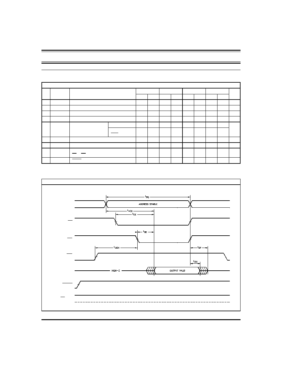
READ-ONLY TIMING
A0 - A20
CE
OE
WE
I/O0 - I/O7
RESET
RY/BY
0V
AC OPERATING CONDITIONS AND CHARACTERISTICS - Read-Only Operations
No.
Symbol
Parameter
70ns*
90ns
120ns
150ns
Unit
Min.
Max.
Min.
Max.
Min.
Max.
Min.
Max.
1
t
RC
Read Cycle Time
6
70
90
120
150
ns
2
t
ACC
Address to Output Delay
70
90
120
150
ns
3
t
CE
Chip Enable to Output Delay
70
90
120
150
ns
4
t
OE
Chip Enable to Output Delay
40
40
50
55
ns
5
t
OEH
Output Enable
Hold Time
6
Read
0
0
0
0
ns
Toggle and
Data Polling
10
10
10
10
6
t
DF
Chip Enable to Output in HIGH-Z
6
20
20
30
35
ns
7
t
DF
Output Enable to Output in HIGH-Z
6
20
20
30
35
ns
8
t
OH
Output Hold Time from Addresses
CE or OE Whichever Occurs First
0
0
0
0
ns
9
t
READY
RESET Pin Low to Read Mode
6
20
20
20
20
µ
s
* V
DD
= 5.0V
±
5%.
30A161-A1
Rev. A
15
DP5Z2MX8PAn3
Dense-Pac Microsystems, Inc.
PRELIMINARY
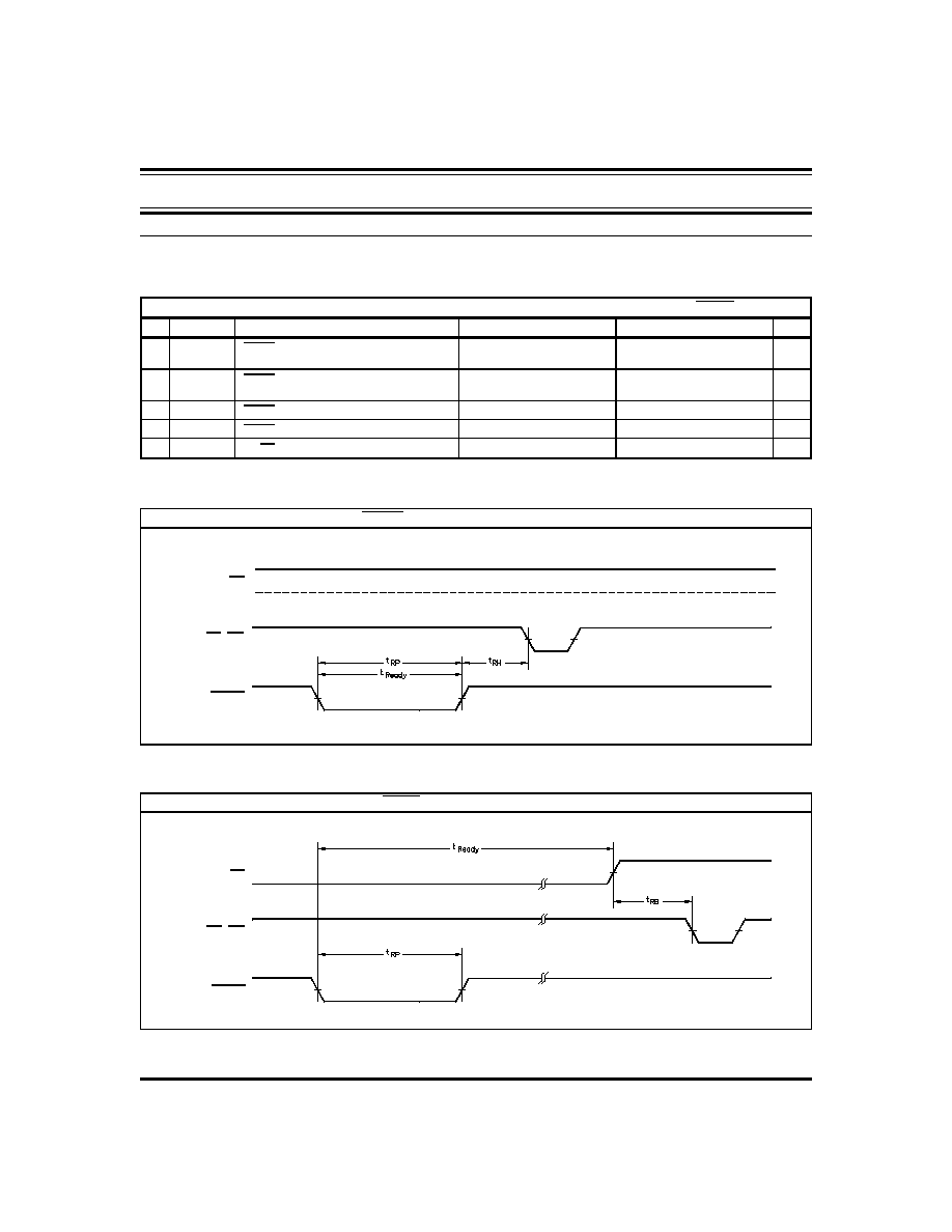
HARDWARE RESET (RESET): Reset Timing NOT During Embedded Algorithm.
RY/BY
CE, OE
RESET
HARDWARE RESET (RESET): Reset Timing During Embedded Algorithm.
RY/BY
CE, OE
RESET
AC OPERATING CONDITIONS AND CHARACTERISTICS - HARDWARE RESET (RESET)
No.
Symbol
Parameter
Min.
Max.
Unit
10
t
READY
RESET Pin Low (During Embedded
Algorithms) to Read or Write
6
20
µ
s
11
t
READY
RESET Pin Low (NOT During Embedded
Algorithms) to Read or Write
6
500
ns
12
t
RP
RESET Pulse Width
500
ns
13
t
RH
RESET High Time before Read
6
50
ns
14
t
RB
RY/BY Recovery Time
0
ns
30A161-A1
Rev. A
16

Dense-Pac Microsystems, Inc.
DP5Z2MX8PAn3
PRELIMINARY
PROGRAM OPERATION TIMINGS
A0 - A20
CE
OE
WE
I/O0 - I/O7
RY/BY
V
DD
NOTE: PA = Program Address, PD = Program Data, D
OUT
is the true data at the program address.
AC OPERATING CONDITIONS AND CHARACTERISTICS - ERASE/PROGRAM OPERATION
No. Symbol
Parameter
70ns*
90ns
120ns
150ns
Unit
Min. Typ. Max. Min. Typ. Max. Min. Typ. Max. Min. Typ. Max.
15
t
WC
Write Cycle Time
6
70
90
120
150
ns
16
t
AS
Address Set-up Time
0
0
0
0
ns
17
t
AH
Address Hold Time
40
45
50
50
ns
18
t
DS
Data Setup Time
40
45
50
50
ns
19
t
DH
Data Hold Time
0
0
0
0
ns
20
t
OES
Output Enable Setup Time
0
0
0
0
ns
21
t
GHWL
Read Recover Time before Write
(OE High to WE Low)
0
0
0
0
ns
22
t
CS
Chip Enable Setup Time
0
0
0
0
ns
23
t
CH
Chip Enable Hold Time
0
0
0
0
ns
24
t
WP
Write Pulse Width
40
45
50
50
ns
25
t
WPH
Write Pulse Width High
20
20
20
20
ns
26
t
WHWH1
Byte Programming Operation
7
7
7
7
µ
s
27
t
WHWH2
Sector Erase Operation
1
8
1
8
1
8
1
8
sec
28
t
VCS
V
DD
setup Time
6
50
50
50
50
µ
s
29
t
BUSY
Write Enable to RY/BY Valid
40
40
40
40
ns
* V
DD
= 5.0V
±
5%.
30A161-A1
Rev. A
17

DP5Z2MX8PAn3
Dense-Pac Microsystems, Inc.
PRELIMINARY
DATA POLLING TIMINGS (During Embedded Algorithms)
CHIP/SECTOR ERASE OPERATION TIMINGS
A0 - A20
CE
OE
WE
I/O0 - I/O7
RY/BY
V
DD
NOTE: When different from Sector Erase, Chip Erase listed in parentheses. SA = Sector Address. VA = Valid Address for reading status data.
A0 - A20
CE
OE
WE
I/O7
1
I/O0 - I/O6
1
RY/BY
NOTE: VA = Valid Address. Illustration shows first two status cycle after command sequence, last status read cycle, and array data read cycle.
30A161-A1
Rev. A
18

Dense-Pac Microsystems, Inc.
DP5Z2MX8PAn3
PRELIMINARY
TOGGLE BIT TIMING (During Embedded Algorithm)
A0 - A20
CE
OE
WE
I/O6, I/O2
RY/BY
NOTE: VA = Valid Address; not required for I/O6
1
. Illustration shows first two status cycle after command sequence, last status read cycle, and array data read cycle.
I/O2 vs. I/O6
WE
I/O6
I/O2
30A161-A1
Rev. A
19
DP5Z2MX8PAn3
Dense-Pac Microsystems, Inc.
PRELIMINARY
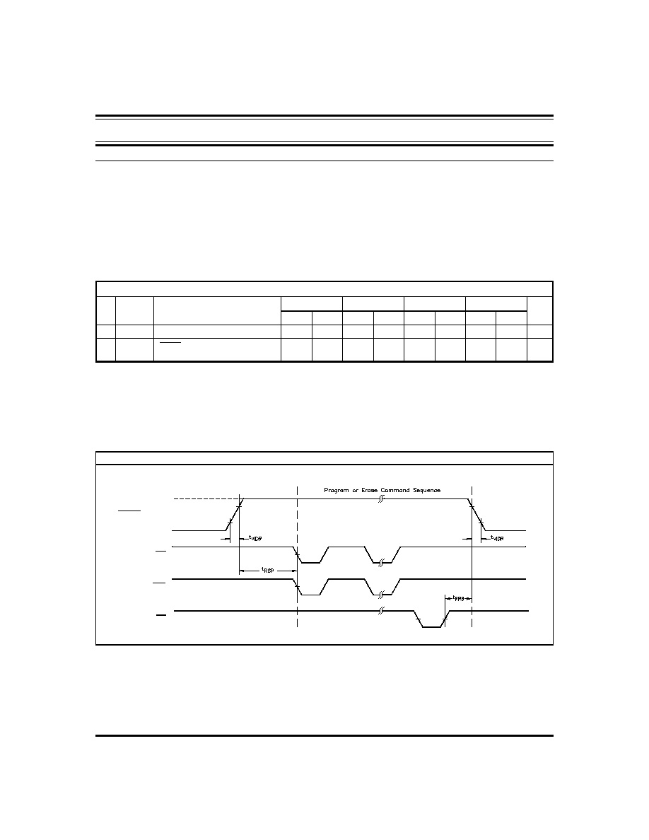
TEMPORARY SECTOR GROUP UNPROTECT TIMINGS
12V
RESET
0 or 5V
CE
WE
RY/BY
AC OPERATING CONDITIONS AND CHARACTERISTICS - TEMPORARY SECTOR UNPROTECT
No. Symbol
Parameter
70ns
90ns
12ns
150ns
Unit
Min.
Max.
Min.
Max.
Min.
Max.
Min.
Max.
30
t
VIDR
V
ID
Rise and Fall Rime
6
500
500
500
500
ns
31
t
RSP
RESET Setup Time for Temporary
Sector Unprotect
4
4
4
4
µ
s
* V
DD
= 5.0V
±
5%.
30A161-A1
Rev. A
20

Dense-Pac Microsystems, Inc.
DP5Z2MX8PAn3
PRELIMINARY
ALTERNATE CE CONTROLLED WRITE OPERATION TIMINGS
A0 - A20
WE
OE
CE
I/O0 - I/O7
RESET
RY/BY
Notes: 1. 555 for Program, 2AA for Erase.
2. Program Address for Program, Sector Address for Sector Erase, 555 for Chip Erase.
3. A0 for Program, 55 for Erase.
4. Program Data for Program, 30 for Sector Erase, 10 for Chip Erase.
5. PA =Program Address, I/O7 = Complement of Data Input, D
OUT
= Array Data.
AC OPERATING CONDITIONS AND CHARACTERISTICS - ERASE/PROGRAM OPERATION
No. Symbol
Parameter
70ns*
90ns
120ns
150ns
Unit
Min. Typ. Max. Min. Typ. Max. Min. Typ. Max. Min. Typ. Max.
32
t
WC
Write Cycle Time
6
70
90
120
150
ns
33
t
AS
Address Set-up Time
0
0
0
0
ns
34
t
AH
Address Hold Time
40
45
50
50
ns
35
t
DS
Data Setup Time
40
45
50
50
ns
36
t
DH
Data Hold Time
0
0
0
0
ns
37
t
GHEL
Read Recover Time before Write
0
0
0
0
ns
38
t
WS
Chip Enable Setup Time
0
0
0
0
ns
39
t
WH
Chip Enable Hold Time
0
0
0
0
ns
40
t
CP
Write Pulse Width
40
45
50
50
ns
41
t
CPH
Write Pulse Width High
20
20
20
20
ns
42
t
WHWH1
Byte Programming Operation
7
7
7
7
µ
s
43
t
WHWH2
Sector Erase Operation
1
8
1
8
1
8
1
8
sec
* V
DD
= 5.0V
±
5%.
See the "Erase and Programming Performance" Section for more information.
30A161-A1
Rev. A
21
DP5Z2MX8PAn3
Dense-Pac Microsystems, Inc.
PRELIMINARY
(48 - Pin Leadless SLCC) MECHANICAL DIAGRAM
(48 - Pin Straight Leaded SLCC) MECHANICAL DIAGRAM
30A161-A1
Rev. A
22

Dense-Pac Microsystems, Inc.
DP5Z2MX8PAn3
PRELIMINARY
(48 - Pin "J" Leaded SLCC) MECHANICAL DIAGRAM
(48 - Pin Gullwing Leaded SLCC) MECHANICAL DIAGRAM
30A161-A1
Rev. A
23
DP5Z2MX8PAn3
Dense-Pac Microsystems, Inc.
PRELIMINARY
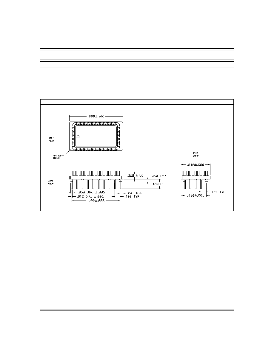
(50 - Pin PGA) MECHANICAL DIAGRAM
30A161-A1
Rev. A
24

Dense-Pac Microsystems, Inc.
DP5Z2MX8PAn3
PRELIMINARY
PART NUMBERING SYSTEM
* V
DD
= 5.0V
±
5%.
Dense-Pac Microsystems, Inc.
7321 Lincoln Way, Garden Grove, California 92841-1431
(714) 898-0007 u (800) 642-4477 u FAX: (714) 897-1772 u http://www.dense-pac.com
Notes:
1. All voltages are with respect to V
SS
.
2. Minimum DC voltage on input or I/O pins is -0.5 V. During voltage
transitions, inputs may overshoot V
SS
to -2.0V for periods of up to
20ns. Maximum DC voltage on output and I/O pins is V
DD
+0.5V.
During voltage transitions, outputs may overshoot to V
DD
+2.0V for
periods up to 20ns.
3. Minimum DC input voltage on A9, OE, RESET pins is -0.5V. During
voltage transitions, A9, OE, RESET pins may overshoot V
SS
to -2.0V
for periods of up to 20ns. See Maximum DC Input Voltage on A9,
OE, and RESET is 12.5V which may overshoot to 13.5V for periods
up to 20ns.
4. No more than one output shorted at a time. Duration of the short
circuit should not be greater than one second.
5. Stresses greater than those under ABSOLUTE MAXIMUM
RATINGS may cause permanent damage to the device. This is a
stress rating only and functional operation of the device at these or
any other conditions above those indicated in the operational
sections of this specification is not implied. Exposure to absolute
maximum rating conditions for extended periods may affect
reliability.
6. This parameter is guaranteed and not 100% tested.
7. The I
CC
current listed includes both the DC Operating Current and
the frequency dependent component (at 6MHz). The frequency
component typically is less than 1mA/MHz, with OE at V
IH
.
8. I
CC
active while Embedded Program or Embedded Erase algorithm
is in progress.
WAVEFORM KEY
Data Valid
Transition from
Transition from
Input = Don't Care
Input = Don't Care
(Steady)
HIGH to LOW
LOW to HIGH
Output = Undefined
Output = Center Line
is HIGH-Z
30A161-A1
Rev. A
25