PIN NAMES
A0-A11
Row Address:
A0-A11
Column Address: A0-A9, A11
BA0,BA1
Bank Select Address
A10/AP
Auto Precharge
DQ0-DQ7
Data In/Data Out
CAS
Column Address Strobe
CS0, CS1
Chip Select
RAS
Row Address Strobe
WE
Data Write Enable
CK, CK
Differential Clock Inputs
CKE0, CKE1
Clock Enable
DQS
Data Strobe
DM
Data Masks
V
DD
Power Supply
V
SS
Ground
V
DDQ
DQ Power Supply
V
SSQ
DQ Ground
V
REF
SSTL_2 Reference Voltage
DNU
Do Not Use
NC
No Connect
This document contains information on a product under consideration for development at DPAC Technologies Corp.
DPAC reserves the right to change or discontinue information on this product without prior notice.
30A242-00
REV. B 2/03
256 Megabit CMOS DDR SDRAM
DPDD32MX8TSBY5
1
ADVAN C E D C O M P O N E NTS PAC K AG I N G
A
D
V
A
N
C
E
D
I
NFO
RM
A
T
I
O
N
DESCRIPTION:
The Memory StackTM series is a family of interchangeable memory devices. The 256 Mb, CMOS DDR Synchronous DRAM
assembly utilizes the space saving LP-StackTM technology to increase memory density. This stack is constructed with two 128Mb
(16M x 8) DDR SDRAMs.
This 256 Mb LP-StackTM, has been designed to fit in the same
footprint as the 128Mb (16M x 8) DDR SDRAM TSOPII
monolithic. This allows system upgrade without electrical or
mechanical redesign, providing an alternative low cost memory
solution.
FEATURES:
∑
Electrical characteristics meet semiconductor
manufacturers' datasheet
∑
Memory organization:
(2) 128Mb memory devices. Each device arranged
as 16M x 8 bits (4M x 8 bits x 4 banks)
∑
Memory stack organization:
32M x 8 bits (8M x 8 bits x 4 banks)
∑
JEDEC approved, 2 Rank stack pinout and footprint
(with 2 CSs and 2 CKEs)
∑
Optimized for RDIMMs
∑
IPC-A-610, class 2, manufacturing standards
∑
Lead free manufacturing process
∑
Package: 66-Pin TSOPII stack
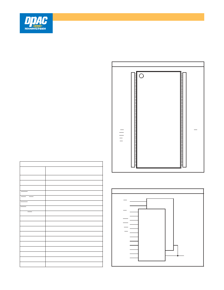
FUNCTIONAL BLOCK DIAGRAM
DM
CAS
WE
DQ0-DQ7
CS0
RAS
CK
DQS
CS1
CK
A0-A11
VREF
CKE1
CKE0
BA0-BA1
(4M x 8 bits x 4 banks)
128 Mb DDR SDRAM
(4M x 8 bits x 4 banks)
PINOUT DIAGRAM
1
(TOP VIEW)
60
NC
VDD
1
2
54
NC
VDDQ
3
53
NC
4
52
VSSQ
DQ1
5
51
DQS
VSSQ
6
50
DNU
NC
7
49
VREF
8
48
VSS
VDDQ
9
47
NC
10
46
CK
DQ3
11
45
CK
VSSQ
12
44
CKE0
NC
13
43
CKE1
NC
14
42
NC
VDDQ
15
41
A11
NC
16
40
A9
NC
17
39
A8
VDD
18
38
A7
DNU
19
37
A6
NC
20
36
A5
WE
21
35
A4
CAS
22
34
VSS
RAS
23
59
DQ5
CS0
24
57
VSSQ
CS1
25
57
NC
BA0
26
56
DQ4
BA1
27
55
VDDQ
DQ2
DQ0
DM
NC
33
VDD
32
A3
31
A2
30
A1
29
A0
28
A10/AP
VDDQ
61
DQ6
62
NC
63
VSSQ
64
DQ7
65
VSS
66
2
DPAC Technologies Products & Services for the Integration Age
7321 Lincoln Way, Garden Grove, CA 92841 Tel 714 898 0007 Fax 714 897 1772
www.dpactech.com Nasdaq: DPAC
©2003 DPAC Technologies, all rights reserved. DPAC TechnologiesTM, Memory StackTM, System StackTM, LP-StackTM, CS-StackTM are trademarks of DPAC Technologies Corp.
DPDD32MX8TSBY5
256 Megabit CMOS DDR SDRAM
30A242-00
REV. B 2/03
A
D
V
A
N
C
E
D
I
NFO
RM
A
T
I
O
N
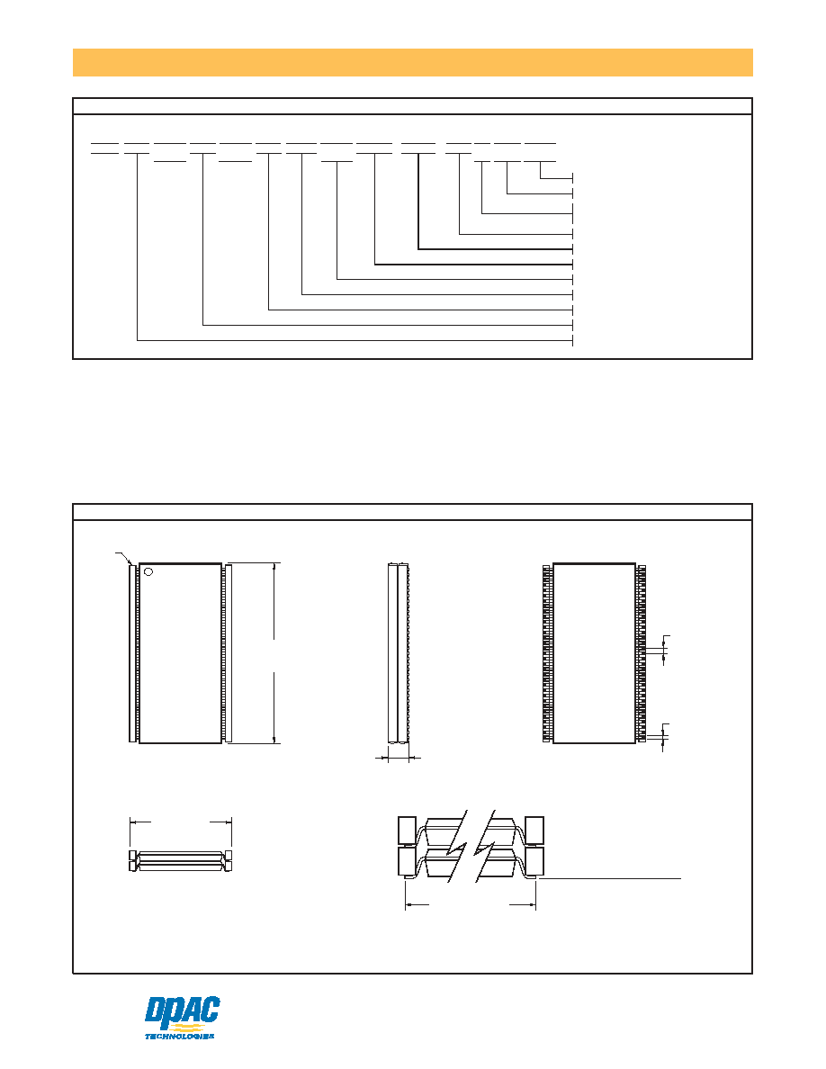
MECHANICAL DIAGRAM
1
.015 [.18]
.0256 [.65]
.102 MAX [2.59 MAX]
PIN 1
INDEX
TOP VIEW
SIDE VIEW
BOTTOM VIEW
END VIEW
.502±.008
.891 MAX.
[12.75±.20]
[22.63 MAX.]
TYP
TYP
END VIEWDETAIL
.463 [11.76] TYP
Lead Toe-to-Toe per device datasheet
Inch [mm]
.004 [.10] from seating plane
COPLANARITY:
ORDERING INFORMATION
DP
X
-
MFR
DOUBLE DATA RATE SYNCHRONOUS DRAM
PREFIX
DD 32M
X
8
Y5
PACKAGE
MEMORY
DESIG
MEMORY
TYPE
MEMORY MODULE WITHOUT SUPPORT LOGIC
DEPTH
WIDTH
DESIG
T
128 MEGABIT BASED
STACKABLE TSOP
MANUFACTURER CODE *
XX
-
MFR ID
SUPPLIER
DP
SUPPLIER CODE *
I/O TYPE
S
SSTL INPUTS/OUTPUTS
WIDTH
DEVICE
B
x8 MEMORY BASED
CLOCK
XX
SPEED
REV
REVISION NOT SPECIFIED
MANUFACTURER DIE REVISION
BLANK
X
XX
LATENCY
CAS
CAS LATENCY
CLOCK SPEED (ns)
* Contact your sales representative for supplier and manufacturer codes.
NOTES:
1. AC Parameters of base memory are unchanged from device manufacturers' specifications.
2. DC Parameters may be affected by stacking. Please refer to application note 53A004-00 for further information.
3. For assembly and inspection procedures, refer to application note 53A001-00.
4. Maximum reflow temperature recommendation is 215∞C.