 | –≠–ª–µ–∫—Ç—Ä–æ–Ω–Ω—ã–π –∫–æ–º–ø–æ–Ω–µ–Ω—Ç: DPS512S8P | –°–∫–∞—á–∞—Ç—å:  PDF PDF  ZIP ZIP |

4 Megabit CMOS SRAM
DPS512S8P/DPS512S8PL/DPS512S8PLL
DESCRIPTION:
The DPS512S8P/PL/PLL is a 512K X 8 high-density,
low-power static RAM module comprised of four
128K X 8 monolithic SRAM's, an advanced
high-speed CMOS decoder and decoupling capacitors
surface mounted on a co-fired ceramic substrate
having side-brazed leads.
The DPS512S8P/PL/PLL is available in a 600-mil-wide,
32-pin dual-in-line package that conforms to the same
JEDEC standard pin configuration as the future four
megabit monolithics.
The DPS512S8P/PL/PLL operates from a single +5V
supply and all input and output pins are completely
TTL-compatible. The low standby power of the
DPS512S8P/PL/PLL makes it ideal for battery-backed
applications.
FEATURES:
∑
524, 288 by 8 Bit Configuration
∑
Access Times: 70*, 85, 100, 120, 150ns
∑
Low Power Dissipation:
25
µ
W (typ.) Standby (DPS512S8PL/DPS512S8PLL)
40
µ
W (typ.) Standby (DPS512S8P)
375 mW (typ.) Operating
∑
2-Volt Data Retention
∑
Fully Static Operation - No Clock or Refresh
Required
∑
All inputs and Outputs are TTL-Compatible
∑
600 mil, 32-pin JEDEC Standard DIP Pinout
*
Available in Commercial only.
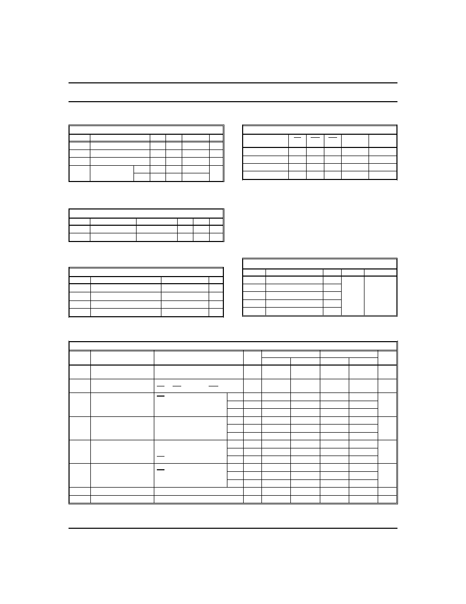
PIN NAMES
A0 - A18
Address Inputs
I/O0 - I/O7
Data In/Out
CE
Chip Enable
WE
Write Enable
OE
Output Enable
V
DD
Power (+5V)
V
SS
Ground
PIN-OUT DIAGRAM
FUNCTIONAL BLOCK DIAGRAM
This document contains information on a product that is currently released
to production at Dense-Pac Microsystems, Inc. Dense-Pac reserves the
right to change products or specifications herein without prior notice.
30A034-00
REV. E
1
DPS512S8P/PL/PLL
Dense-Pac Microsystems, Inc.
DC OUTPUT CHARACTERISTICS
Symbol
Parameter
Conditions
Min. Max. Unit
V
OH
HIGH Voltage
I
OH
= -1.0mA 2.4
-
V
V
OL
LOW Voltage
I
OL
= 2.1mA
0.4
V
ABSOLUTE MAXIMUM RATINGS
3
Symbol
Parameter
Max.
Unit
T
STC
Storage Temperature
-55 to +125
∞
C
T
BIAS
Temperature Under Bias
-10 to + 85
∞
C
V
DD
Supply Voltage
1
-0.5 to + 7.0
V
V
I/O
Input/Output Voltage
1
-0.5 to V
DD
+0.5 V
TRUTH TABLE
Mode
CE
WE
OE
I/O Pin
Supply
Current
Not Selected
H
X
X
HIGH-Z Standby
D
OUT
Disable
L
H
H
HIGH-Z
Active
Read
L
H
L
D
OUT
Active
Write
L
L
X
D
IN
Active
H = HIGH L = LOW X = Don't Care
CAPACITANCE
4
: T
A
= 25
∞
C, F = 1.0MHz
Symbol
Parameter
Max.
Unit
Condition
C
ADR
Address Input
45
pF
V
IN
= 0V
C
CE
Chip Enable
20
C
WE
Write Enable
45
C
OE
Output Enable
45
C
I/O
Data Input/Output
50
DC OPERATING CHARACTERISTICS: Over operating ranges
Symbol
Characteristics
Test Conditions
TYP.
COMMERCIAL
INDUSTRIAL
Unit
Min.
Max.
Min.
Max.
I
IN
Input
Leakage Current
V
IN
= 0V to V
DD
-
-10
+10
-10
+10
µ
A
I
OUT
Output
Leakage Current
V
I/O
= 0V to V
DD
,
CE or OE = V
IH
, or WE = V
IL
-
-10
+10
-10
+10
µ
A
I
CC1
Active
Supply Current
CE = V
IL
,
V
IN
= V
IH
or V
IL
,
I
OUT
= 0mA
P
30
50
55
mA
PL
30
50
55
PLL
30
40
45
I
CC2
Operating
Supply Current
Cycle = min.,
Duty = 100%,
I
OUT
= 0mA
P
75
110
110
mA
PL
60
100
100
PLL
40
80
80
I
SB1
Full Standby
Supply Current
V
IN
V
DD
-0.2V or
V
IN
V
SS
+0.2V,
CE
V
DD
-0.2V
P
8
400
600
µ
A
PL
5
200
300
PLL
5
100
200
I
SB2
Standby Current
CE = V
IH
,
V
IN
= V
IH
or V
IN
P
4
12
12
mA
PL
4
8
10
PLL
4
6
8
V
OL
Output Low Voltage
I
OUT
= 2.1mA
-
0.4
0.4
V
V
OH
Output High Voltage
I
OUT
= -1.0mA
-
2.4
2.4
V
Not available in 70ns.
RECOMMENDED OPERATING RANGE
1
Symbol
Characteristic
Min. Typ.
Max.
Unit
V
DD
Supply Voltage
4.5
5.0
5.5
V
V
IH
Input HIGH Voltage
2.2
V
DD
+0.3 V
V
IL
Input LOW Voltage
-0.5
2
0.8
V
T
A
Operating
Temperature
C
0
+25
+70
∞
C
I
-40 +25
+85
30A034-00
REV. E
2
Dense-Pac Microsystems, Inc.
DPS512S8P/PL/PLL
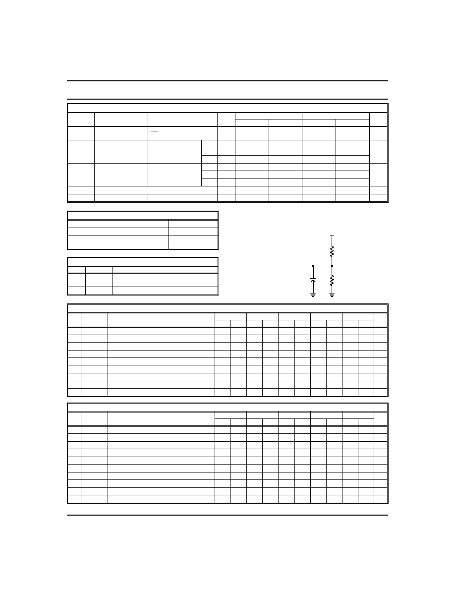
Figure 1. Output Load
** Including Probe and Jig Capacitance.
+5V
990
1.8K
C
L
**
D
OUT
Output Load
Load
C
L
Parameters Measured
1
100pF
except t
CLZ
, t
OLZ
, t
CHZ
, t
OHZ
, t
WHZ
,
and t
WLZ
2
5pF
t
CLZ
, t
OLZ
, t
CHZ
, t
OHZ
, t
WHZ
, and t
WLZ
AC TEST CONDITIONS
Input Pulse Levels
0V to 3.0V
Input Pulse Rise and Fall Times
5ns *
Input and Output
Timing Reference Levels
1.5V
* Transition measured between 0.8V and 2.2V.
AC OPERATING CONDITIONS AND CHARACTERISTICS - READ CYCLE: Over operating ranges
No. Symbol
Parameter
70ns
85ns
100ns
120ns
150ns
Unit
Min. Max. Min. Max. Min. Max. Min. Max. Min. Max.
1
t
RC
Read Cycle Time
70
85
100
120
150
ns
2
t
AA
Address Access Time
70
85
100
120
150 ns
3
t
CO
Chip Enable to Output Valid
70
85
100
120
150 ns
4
t
OV
Output Enable to Output Valid
45
45
45
50
60
ns
5
t
OH
Output Hold from Address Change
10
10
10
10
10
ns
6
t
CLZ
Chip Enable to Output in LOW-Z
4, 6
5
5
5
5
5
ns
7
t
OLZ
Output Enable to Output in LOW-Z
4, 6
0
0
0
0
0
ns
8
t
CHZ
Chip Enable to Output in HIGH-Z
4, 6
35
45
45
50
60
ns
9
t
OHZ
Output Enable to Output in HIGH-Z
4, 6
30
30
30
35
45
ns
AC OPERATING CONDITIONS AND CHARACTERISTICS - WRITE CYCLE: Over operating ranges
7
No. Symbol
Parameter
70ns
85ns
100ns
120ns
150ns
Unit
Min. Max. Min. Max. Min. Max. Min. Max. Min. Max.
10
t
WC
Write Cycle Time
70
85
100
120
150
ns
11
t
AW
Address Valid to End of Write
65
80
90
105
115
ns
12
t
CW
Chip Enable to End of Write
65
80
90
105
115
ns
13
t
DW
Data to Write Time Overlap
35
35
35
40
50
ns
14
t
DH
Data Hold Time from Write Time
0
0
0
0
0
ns
15
t
WP
Write Pulse Width
55
55
65
75
85
ns
16
t
AS
Address Set-up Time ***
0
0
0
0
0
ns
17
t
AH
Address Hold Time
5
5
5
5
5
ns
18
t
WHZ
Write Enable to Output in HIGH-Z
4, 6
30
30
30
35
40
ns
19
t
WLZ
Write Enable to Output in LOW-Z
4, 6
5
5
5
5
5
ns
*** Valid for both Read and Write Cycles.
Available in commercial only.
DATA RETENTION CHARACTERISTICS
Symbol
Parameter
Test Conditions
Typ.
COMMERCIAL
INDUSTRIAL
Unit
Min.
Max.
Min.
Max.
V
DR
Data Retention
Voltage
CE
V
DR
-0.2V
-
2.0
5.5
2.0
5.5
V
I
CCDR2
Data Retention
Supply Current
V
DR
= 2.0V
P
4
180
270
µ
A
PL
4
80
120
PLL
1
40
60
I
CCDR3
Data Retention
Supply Current
V
DR
= 3.0V
P
4
200
300
µ
A
PL
4
100
150
PLL
1
50
75
t
CDR
Chip Disable to Data Retention Time
-
0
0
ns
t
R
Recovery Time
t
RC
= Read Cycle Timing
5
5
ms
Not Available in 70ns.
30A034-00
REV. E
3

DPS512S8P/PL/PLL
Dense-Pac Microsystems, Inc.
READ CYCLE 2:
CE Controlled. WE is HIGH.
ADDRESS
CE
OE
DATA I/O
READ CYCLE 1:
Address Controlled. WE is HIGH. CE and OE are LOW.
ADDRESS
DATA I/O
DATA RETENTION WAVEFORM
CE
V
DR
2.2V
V
SS
V
DD
4.5V
30A034-00
REV. E
4

Dense-Pac Microsystems, Inc.
DPS512S8P/PL/PLL
WRITE CYCLE 2:
CE Controlled. OE is HIGH.
ADDRESS
CE
WE
DATA I/O
WAVEFORM KEY
Data Valid
Transition from
Transition from
Data Undefined
HIGH to LOW
LOW to HIGH
or Don't Care
WRITE CYCLE 1
:
WE Controlled. OE is LOW.
ADDRESS
CE
WE
DATA I/O
30A034-00
REV. E
5