8 Megabit High Speed CMOS SRAM
DPS512X16Cn3/DPS512X16Bn3
DESCRIPTION:
The DPS512X16Cn3/DPS512X16Bn3 High Speed SRAM `'STACK''
modules are a revolutionary new memory subsystem using Dense-Pac
Microsystems' ceramic Stackable Leadless Chip Carriers (SLCC).
Available in straight leaded, `'J'' leaded or gullwing leaded packages,
or mounted on a 50-pin PGA co-fired ceramic substrate. The module
packs 8-Megabits of low-power CMOS static RAM in an area as small
as 0.463 in
2
, while maintaining a total height as low as 0.705 inches.
The DPS512X16Cn3/DPS512X16Bn3 STACK modules contain eight
individual 128K x 8 SRAMs, each packaged in a hermetically sealed
SLCC, making the modules suitable for commercial, industrial and
military applications.
The DPS512X16Bn3 has one active low Chip Enable (CE) and while
the DPS512X16Cn3 an active low Chip Enable (CE) and an active high
Select Line (SEL).
By using SLCCs, the `'Stack'' family of modules offer a higher board
density of memory than available with conventional through-hole,
surface mount or hybrid techniques.
FEATURES:
∑
Organizations Available: 512Kx16 or 1024Kx8
∑
Access Times: 20*, 25, 30, 35, 45ns
∑
Fully Static Operation - No clock or refresh required
∑
Single +5V Power Supply,
±
10% Tolerance
∑
TTL Compatible
∑
Common Data Inputs and Outputs
∑
Low Data Retention Voltage: 2.0V min.
∑
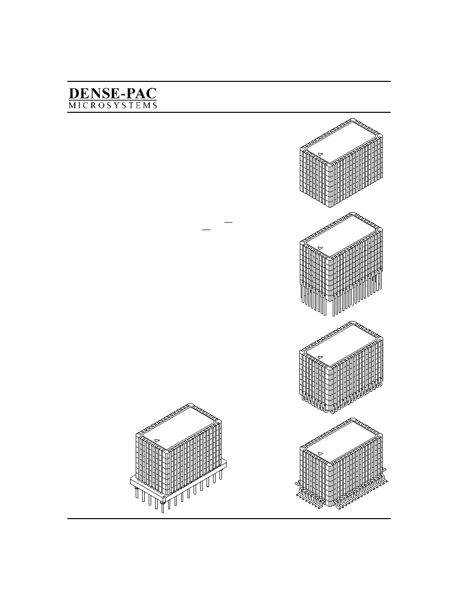
Packages Available:
48 - Pin SLCC Stack
48 - Pin Straight Leaded Stack
48 - Pin `'J'' Leaded Stack
48 - Pin Gullwing Leaded Stack
50 - Pin PGA Dense-Stack
*
Commercial only.
`'J'' Leaded
Stack
Gullwing
Leaded Stack
Dense-Stack
SLCC Stack
Straight Leaded
Stack
This document contains information on a product that is currently released
to production at Dense-Pac Microsystems, Inc. Dense-Pac reserves the
right to change products or specifications herein without prior notice.
30A097-38
REV. D
1

DPS512X16Cn3/DPS512X16Bn3
Dense-Pac Microsystems, Inc.
PIN-OUT DIAGRAM
NOTE: SEL0 and SEL1 apply to DPS512X16Cn3 version only, No Connect for DPS512X16Bn3 version.
PIN NAMES
A0 - A16
Address Inputs
I/O0 - I/O15
Data Input/Output
CE0 - CE7
Low Chip Enables
SEL0, SEL1
High Chip Enables
WE
Write Enable
OE
Output Enable
V
DD
Power (+5V)
V
SS
Ground
N.C.
No Connect
FUNCTIONAL BLOCK DIAGRAM
NOTE: SEL0 and SEL1 apply to DPS512X16Cn3 version only.
48 - PIN LEADLESS STACK
48 - PIN STRAIGHT LEADED STACK
48 - PIN `'J'' LEADED STACK
48 - PIN GULLWING LEADED STACK
50 - PIN PGA
DENSE-STACK
30A097-38
REV. D
2

Dense-Pac Microsystems, Inc.
DPS512X16Cn3/DPS512X16Bn3
RECOMMENDED OPERATING RANGE
3
Symbol
Characteristic
Min. Typ.
Max.
Unit
V
DD
Supply Voltage
4.5
5.0
5.5
V
V
IH
Input HIGH Voltage 2.2
V
DD
+0.3 V
V
IL
Input LOW Voltage -0.5
2
0.8
V
T
A
Operating
Temperature
M/B -55 +25
+125
o
C
I
-40 +25
+85
C
0
+25
+70
TRUTH TABLE
Mode
SEL
CE
WE
OE I/O Pin Supply
Current
Not Selected
L
X
X
X
High-Z Standby
Not Selected
X
H
X
X
High-Z Standby
D
OUT
Disable
H
L
H
H
High-Z Active
Read
H
L
H
L
D
OUT
Active
Write
H
L
L
X
D
IN
Active
H = HIGH L = LOW X = Don't Care
NOTE: SEL applies to DPS512X16Cn3 version only.
DC OUTPUT CHARACTERISTICS
Symbol
Parameter
Conditions
Min. Max. Unit
V
OH
HIGH Voltage
I
OH
= -4.0mA 2.4
V
V
OL
LOW Voltage
I
OL
=8.0mA
0.4
V
ABSOLUTE MAXIMUM RATINGS
3
Symbol
Parameter
Value
Unit
T
STC
Storage Temperature
-65 to +150
∞
C
T
BIAS
Temperature Under Bias
-55 to +125
∞
C
V
DD
Supply Voltage
1
-0.5 to +7.0
∞
C
V
I/O
Input/Output Voltage
1
-0.5 to V
DD
+0.5
V
DC OPERATING CHARACTERISTICS:
Over operating ranges
Symbol
Characteristics
Test Conditions
Typ.
()
C
I
M
Unit
Min.
Max.
Min.
Max.
Min.
Max.
I
IN
Input
Leakage Current
V
IN
= 0V to V
DD
-
-40
+40
-40
+40
-40
+40
µ
A
I
OUT
Output
Leakage Current
V
I/O
= 0V to V
DD
,
CE or OE = V
IH
, or WE = V
IL
-
-40
+40
-40
+40
-40
+40
µ
A
I
CC
Operating
Supply Current
Cycle=min., Duty=100%
I
OUT
= 0mA
X8
275
350
385
405
mA
X16
350
460
490
530
I
SB1
Full Standby
Supply Current
V
IN
V
DD
-0.2V or
V
IN
V
SS
+0.2V
3.2
40
40
80
mA
I
SB2
Standby Current (TTL)
CE = V
IH
200
240
280
280
mA
I
DR3
Data Retention
Supply Current
(3V)
V
DR
= 3V, CE
V
DR
-0.2V,
(or SEL
0.2V, V
IN
V
DD
-0.2V
or V
IN
+0.2V)
0.56
3.20
4.80
16.00 mA
I
DR2
Data Retention
Supply Current
(2V)
V
DR
= 2V, CE
V
DR
-0.2V,
(or SEL
0.2V, V
IN
V
DD
-0.2V
or V
IN
+0.2V)
0.28
2.00
3.20
14.40 mA
V
OL
Output Low Voltage
I
OUT
= 8.0mA
-
0.4
0.4
0.4
V
V
OH
Output High Voltage
I
OUT
= -4.0mA
-
2.4
2.4
2.4
V
Typical measurements made at +25
o
C, Cycle = min., V
DD
= 5.0V.
NOTE: Test Conditions in parenthesis apply to DPS512X16Cn3 version only.
CAPACITANCE
4
:
T
A
= 25∞C, F = 1.0MHz
Symbol
Parameter
Max.
Unit
Condition
C
ADR
Address Input
100
pF
V
IN
2
= 0V
C
CE
Chip Enable
30
C
SEL
Active High
Chip Select
50
C
WE
Write Enable
100
C
OE
Output Enable
100
C
I/O
Data Input/Output
70
NOTE: C
SEL
applies to DPS512X16Cn3 version only.
30A097-38
REV. D
3

DPS512X16Cn3/DPS512X16Bn3
Dense-Pac Microsystems, Inc.
DATA RETENTION WAVEFORM: SEL Controlled. (Applies to DPS512X16Cn3 only)
DATA RETENTION WAVEFORM:
CE Controlled.
V
DD
4.5V
SEL
V
DR2
0.4V
0V
SEL
-0.2V
V
DD
4.5V
2.3V
V
DR1
CE
0V
CE
V
DD
-0.2V
+5V
255
480
C
L
*
D
OUT
Figure 1.
Output Load
* Including Probe and Jig Capacitance.
OUTPUT LOAD
Load
C
L
Parameters Measured
1
100pF
except t
LZ1
, t
LZ2
, t
HZ1
, t
HZ2
, t
OHZ
, t
OLZ
,
and t
WHZ
2
5pF
t
LZ1
, t
LZ2
, t
HZ1
, t
HZ2
, t
OHZ
, t
OLZ
, and
t
WHZ
NOTE: t
LZ2
and t
HZ2
apply to DPS512X16Cn3 version only.
AC TEST CONDITIONS
Input Pulse Levels
0V to 3.0V
Input Pulse Rise and Fall Times
5ns
Input and Output
Timing Reference Levels
1.5V
Data Retention AC Characteristics
8
Symbol
Parameter
Test Conditions
Min.
Typ.
Max.
Unit
V
DR
V
DD
for Data
Retention
CE
V
DR
-0.2V, (SEL
V
DR
-0.2V,
or V
IN
V
DR
-0.2V or V
IN
0.2V)
2.0
-
-
V
V
CDR
Chip Disable to
Data Retention Time
See Data Retention Waveform
0
-
-
ns
t
R
Operation Recovery Time
See Data Retention Waveform
5
-
-
ms
NOTE: Test Conditions in parenthesis apply to DPS512X16Cn3 version only.
30A097-38
REV. D
4

Dense-Pac Microsystems, Inc.
DPS512X16Cn3/DPS512X16Bn3
READ CYCLE
NOTE: SEL, t
CO2
, t
LZ2
and t
HZ2
apply to DPS512X16Cn3 version only.
ADDRESS
CE
SEL
OE
DATA I/O
WAVEFORM KEY
Data Valid
Transition from
Transition from
Data Undefined
HIGH to LOW
LOW to HIGH
or Don't Care
AC OPERATING CONDITIONS AND CHARACTERISTICS - READ CYCLE:
Over operating ranges
No. Symbol
Parameter
20ns*
25ns
30ns
35ns
45ns
Unit
Min. Max. Min. Max. Min. Max. Min. Max. Min. Max.
1
t
RC
Read Cycle Time
20
25
30
35
45
ns
2
t
AA
Address Access Time
20
25
30
35
45
ns
3
t
CO1
CE to Output Valid
20
25
30
35
45
ns
4
t
CO2
SEL to Output Valid
20
25
30
35
45
ns
5
t
OE
Output Enable to Output Valid
8
10
15
20
25
ns
6
t
LZ1
CE to Output in LOW-Z
4, 5
3
3
3
3
3
ns
7
t
LZ2
SEL to Output in LOW-Z
4, 5
3
3
3
3
3
ns
8
t
OLZ
Output Enable to Output in LOW-Z
4, 5
0
0
0
0
0
ns
9
t
HZ1
CE to Output in HIGH-Z
4, 5
10
12
15
20
25
ns
10
t
HZ2
SEL to Output in HIGH-Z
4, 5
10
12
15
20
25
ns
11
t
OHZ
Output Enable to Output in HIGH-Z
4, 5
8
10
15
20
25
ns
12
t
OH
Output Hold from Address Change
3
3
3
3
3
ns
* Available in Commercial Only.
NOTE: t
CO2
, t
LZ2
and t
HZ2
apply to DPS512X16Cn3 version only.
30A097-38
REV. D
5