DCR1260Y
1/10
www.dynexsemi.com
FEATURES
s
Double Side Cooling
s
High Surge Capability
s
Low Inductance Internal Construction
APPLICATIONS
s
High Power Converters
s
DC Motor Control
s
High Voltage Power Supplies
VOLTAGE RATINGS
ORDERING INFORMATION
When ordering, select the required part number shown in the
Voltage Ratings selection table.
For example:
DCR1260Y63
Note: Please use the complete part number when ordering and
quote this number in any future correspondance relating to your
order.
KEY PARAMETERS
V
DRM
6500V
I
T(AV)
1260A
I
TSM
(max)
20800A
dV/dt
1000V/
µ
s
dI/dt
300A/
µ
s
DCR1260Y
Phase Control Thyristor
Target Information
DS5498-1.2 February 2002
Conditions
T
vj
= 0∞ to 125∞C,
I
DRM
= I
RRM
= 150mA,
V
DRM
, V
RRM
t
p
= 10ms,
V
DSM
& V
RSM
=
V
DRM
& V
RRM
+ 100V
respectively
Lower voltage grades available.
6500
6400
6300
6200
6100
6000
DCR1260Y65
DCR1260Y64
DCR1260Y63
DCR1260Y62
DCR1260Y61
DCR1260Y60
Part and Ordering
Number
Repetitive Peak
Voltages
V
DRM
and V
DRM
V
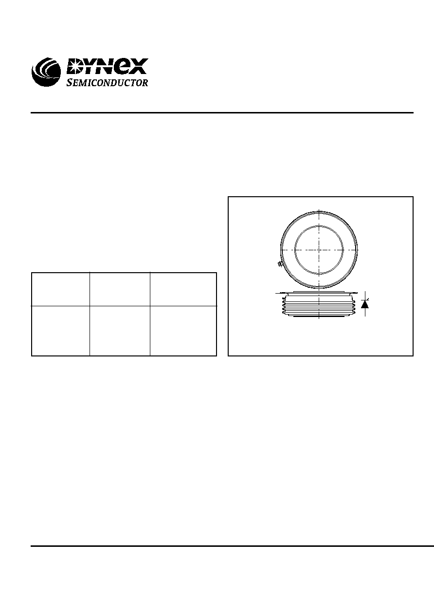
Fig. 1 Package outline
Outline type code: Y
(See Package Details for further information)
DCR1260Y
2/10
www.dynexsemi.com
Symbol
I
T(AV)
I
T(RMS)
I
T
I
T(AV)
I
T(RMS)
I
T
CURRENT RATINGS
T
case
= 60∞C unless stated otherwise.
Test Conditions
Half wave resistive load
-
-
Half wave resistive load
-
-
Units
A
A
A
A
A
A
Max.
1260
1980
1935
863
1356
1254
Parameter
Mean on-state current
RMS value
Continuous (direct) on-state current
Mean on-state current
RMS value
Continuous (direct) on-state current
Single Side Cooled
Double Side Cooled
Symbol
I
T(AV)
I
T(RMS)
I
T
I
T(AV)
I
T(RMS)
I
T
T
case
= 80∞C unless stated otherwise.
Test Conditions
Half wave resistive load
-
-
Half wave resistive load
-
-
Units
A
A
A
A
A
A
Max.
1617
1598
1543
690
1084
983
Parameter
Mean on-state current
RMS value
Continuous (direct) on-state current
Mean on-state current
RMS value
Continuous (direct) on-state current
Single Side Cooled
Double Side Cooled
DCR1260Y
3/10
www.dynexsemi.com
Parameter
Surge (non-repetitive) on-state current
I
2
t for fusing
Surge (non-repetitive) on-state current
I
2
t for fusing
Test Conditions
10ms half sine, T
case
= 125∞C
V
R
= 50% V
RRM
- 1/4 sine
10ms half sine, T
case
= 125∞C
V
R
= 0
Symbol
I
TSM
I
2
t
I
TSM
I
2
t
SURGE RATINGS
Units
kA
A
2
s
kA
A
2
s
Max.
16.7
1.4 x 10
6
20.8
2.18 x 10
6
Parameter
Peak reverse and off-state current
Max. linear rate of rise of off-state voltage
Rate of rise of on-state current
Threshold voltage
On-state slope resistance
Delay time
Turn-off time
Latching current
Holding current
Test Conditions
At V
RRM
/V
DRM
, T
case
= 125∞C
To 67% V
DRM
, T
j
= 125∞C
From 67% V
DRM
,
Repetitive 50Hz
Gate source 30V, 15
,
Non-repetitive
t
r
0.5
µ
s, T
j
= 125∞C
At T
vj
= 125∞C
At T
vj
= 125∞C
V
D
= 67% V
DRM
, gate source 30V, 15
t
r
= 0.5
µ
s, Tj = 25∞C
I
T
= 1000A, t
p
= 1ms, T
j
=125∞C,
V
R
= 100V, dI
RR
/dt = 10A/
µ
s,
V
DR
= 67% V
DRM
,
dV
DR
/dt = 25V/
µ
s linear
T
j
= 25∞C, V
D
= 10V
T
j
= 25∞C
Symbol
I
RRM
/I
RRM
dV/dt
dI/dt
V
T(TO)
r
T
t
gd
t
q
I
L
I
H
DYNAMIC CHARACTERISTICS
Units
mA
V/
µ
s
A/
µ
s
A/
µ
s
V
m
µ
s
µ
s
mA
mA
Max.
300
1000
150
300
1.2
1.18
1.5
-
600
200
Min.
-
-
-
-
-
-
0.5
600
-
-

DCR1260Y
4/10
www.dynexsemi.com
Parameter
Gate trigger voltage
Gate trigger current
Gate non-trigger voltage
Peak forward gate voltage
Peak forward gate voltage
Peak reverse gate voltage
Peak forward gate current
Peak gate power
Mean gate power
Test Conditions
V
DRM
= 5V, T
case
= 25
o
C
V
DRM
= 5V, T
case
= 25
o
C
At V
DRM
T
case
= 125
o
C
Anode positive with respect to cathode
Anode negative with respect to cathode
-
Anode positive with respect to cathode
See table fig. 4
-
Symbol
V
GT
I
GT
V
GD
V
FGM
V
FGN
V
RGM
I
FGM
P
GM
P
G(AV)
GATE TRIGGER CHARACTERISTICS AND RATINGS
Max.
3.0
300
0.25
30
0.25
5
10
150
5
Units
V
mA
V
V
V
V
A
W
W
Parameter
Thermal resistance - junction to case
Thermal resistance - case to heatsink
Virtual junction temperature
Storage temperature range
Clamping force
Test Conditions
Double side cooled
DC
Single side cooled
Anode DC
Cathode DC
Clamping force 50kN
Double side
(with mounting compound)
Single side
On-state (conducting)
Reverse (blocking)
THERMAL AND MECHANICAL RATINGS
Symbol
R
th(j-c)
R
th(c-h)
T
vj
T
stg
F
m
Units
∞CW
∞CW
∞CW
∞CW
∞CW
∞C
∞C
∞C
kN
Max.
0.0095
0.019
0.019
0.002
0.004
135
125
125
55.0
Min.
-
-
-
-
-
-
-
≠55
45.0

DCR1260Y
5/10
www.dynexsemi.com
CURVES
Fig.2 Maximum (limit) on-state characteristics
Fig.3 Power dissipation
0
500
1000
1500
2000
2500
1.5
2.0
2..5
3.5
4.0
Instantaneous on-state voltage, V
T
- (V)
Instantaneous on-state current, I
T
- (A)
3.0
T
j
= 125∞C
0
200
400
600
800
1000
1200
1400
1600
1800
2000
0
100
200
300
400
500
600
700
800
900 1000
Mean on-state current, I
T(AV)
- (A)
Mean power dissipation - (W)
dc
1/2 wave
3 phase
6 phase