1/9
www.dynexsemi.com
DCR1475SY
APPLICATIONS
s
High Power Drives
s
High Voltage Power Supplies
s
DC Motor Control
s
Welding
s
Battery Chargers
FEATURES
s
Double Side Cooling
s
High Surge Capability
VOLTAGE RATINGS
ORDERING INFORMATION
When ordering, select the required part number shown in the
Voltage Ratings selection table.
For example:
DCR1475SY29
Note: Please use the complete part number when ordering
and quote this number in any future correspondance relating
to your order.
KEY PARAMETERS
V
DRM
3000V
I
T(AV)
2805A
I
TSM
46000A
dVdt*
1000V/
µ
s
dI/dt
300A/
µ
s
*Higher dV/dt selections available
DCR1475SY
Phase Control Thyristor
Advance Information
Replaces January 2000 version, DS4246-4.0
DS4246-5.0 July 2001
DCR1475SY30
DCR1475SY29
DCR1475SY28
DCR1475SY27
DCR1475SY26
DCR1475SY25
Conditions
T
vj
= 0∞ to 125∞C,
I
DRM
= I
RRM
= 250mA,
V
DRM
, V
RRM
t
p
= 10ms,
V
DSM
& V
RSM
=
V
DRM
& V
RRM
+ 100V
Respectively
Lower voltage grades available.
Type Number
Repetitive Peak
Voltages
V
DRM
V
RRM
V
3000
2900
2800
2700
2600
2500
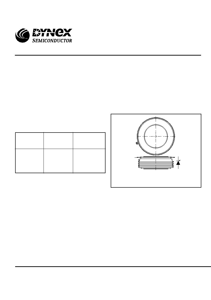
Outline type code: Y
See Package Details for further information.
(The DCR1475 is also available in a thin package, type code V.
Please contact Customer Services for more information).
Fig. 1 Package outline
2/9
www.dynexsemi.com
DCR1475SY
CURRENT RATINGS
T
case
= 80∞C unless staed otherwise.
Symbol
Parameter
Conditions
Double Side Cooled
I
T(AV)
Mean on-state current
I
T(RMS)
RMS value
I
T
Continuous (direct) on-state current
Single Side Cooled (Anode side)
I
T(AV)
Mean on-state current
I
T(RMS)
RMS value
I
T
Continuous (direct) on-state current
Units
Max.
Half wave resistive load
2220
A
-
3490
A
-
3175
A
Half wave resistive load
1420
A
-
2230
A
-
1850
A
CURRENT RATINGS
T
case
= 60∞C unless staed otherwise.
Symbol
Parameter
Conditions
Double Side Cooled
I
T(AV)
Mean on-state current
I
T(RMS)
RMS value
I
T
Continuous (direct) on-state current
Single Side Cooled (Anode side)
I
T(AV)
Mean on-state current
I
T(RMS)
RMS value
I
T
Continuous (direct) on-state current
Units
Max.
Half wave resistive load
2805
A
-
4406
A
-
4101
A
Half wave resistive load
1850
A
-
2906
A
-
2508
A
3/9
www.dynexsemi.com
DCR1475SY
SURGE RATINGS
Conditions
10ms half sine; T
case
= 125
o
C
V
R
= 50% V
RRM
- 1/4 sine
10ms half sine; T
case
= 125
o
C
V
R
= 0
Max.
Units
Symbol
Parameter
I
TSM
Surge (non-repetitive) on-state current
I
2
t
I
2
t for fusing
I
TSM
Surge (non-repetitive) on-state current
I
2
t
I
2
t for fusing
10.6 x 10
6
A
2
s
46.0
kA
6.7 x 10
6
A
2
s
36.8
kA
THERMAL AND MECHANICAL DATA
dc
Conditions
Min.
Max.
Units
o
C/W
-
0.019
Anode dc
Clamping force 43.0kN
with mounting compound
Thermal resistance - case to heatsink
R
th(c-h)
0.002
Double side
-
125
o
C
T
vj
Virtual junction temperature
T
stg
Storage temperature range
Reverse (blocking)
Single side
-
Thermal resistance - junction to case
R
th(j-c)
Single side cooled
Symbol
Parameter
Clamping force
41.0
49.0
kN
≠55
125
o
C
-
On-state (conducting)
-
135
o
C
-
0.004
o
C/W
o
C/W
Cathode dc
-
0.019
o
C/W
Double side cooled
-
0.0095
o
C/W

4/9
www.dynexsemi.com
DCR1475SY
DYNAMIC CHARACTERISTICS
Parameter
Symbol
Conditions
Typ.
Max.
Units
GATE TRIGGER CHARACTERISTICS AND RATINGS
V
DRM
= 5V, T
case
= 25
o
C
Conditions
Parameter
Symbol
V
GT
Gate trigger voltage
V
DRM
= 5V, T
case
= 25
o
C
I
GT
Gate trigger current
V
GD
Gate non-trigger voltage
At V
DRM
T
case
= 125
o
C
V
FGM
Peak forward gate voltage
Anode positive with respect to cathode
V
FGN
Peak forward gate voltage
Anode negative with respect to cathode
V
RGM
Peak reverse gate voltage
I
FGM
Peak forward gate current
Anode positive with respect to cathode
P
GM
Peak gate power
See table, gate characteristics curve
P
G(AV)
Mean gate power
4.0
V
400
mA
0.25
V
30
V
0.25
V
5
V
30
A
150
W
10
W
Max.
Units
I
RRM
/I
DRM
Peak reverse and off-state current
At V
RRM
/V
DRM
, T
case
= 125
o
C
From 67% V
DRM
to 1000A
Gate source 20V, 10
t
r
< 0.5
µ
s. T
j
= 125∞C
dV/dt
Maximum linear rate of rise of off-state voltage
To 67% V
DRM
T
j
= 125
o
C
-
250
mA
-
1000
V/
µ
s
Repetitive, 50Hz
-
150
A/
µ
s
Non-repetitive
-
300
A/
µ
s
Rate of rise of on-state current
dI/dt
V
T(TO)
Threshold voltage
At T
vj
= 125
o
C
r
T
On-state slope resistance
At T
vj
= 125
o
C
t
gd
Delay time
I
L
Latching current
T
j
= 25
o
C, V
D
= 5V
I
H
Holding current
T
j
= 25
o
C, R
g - k
=
0.885
-
V
-
0.191
m
-
2.0
µ
s
V
D
= 67% V
DRM
, Gate source 30V, 15
Rise time 0.5
µ
s, T
j
= 25
o
C
100
300
mA
30
100
mA
I
T
= 800A, t
p
= 1ms, T
j
= 125∞C,
V
RM
= 50V, dI
RR
/dt = 20A/
µ
s,
V
DR
= 67% V
DRM
, dV
DR
/dt = 20V/
µ
s linear
µ
s
-
400
Turn-off time
t
q

5/9
www.dynexsemi.com
DCR1475SY
CURVES
Fig.2 Maximum (limit) on-state characteristics
Fig.3 Dissipation curves
V
TM
Equation:-
V
TM
= A + Bln (I
T
) + C.I
T
+D.
I
T
Where
A = 14.007
B = ≠2.911
C = ≠0.001
D = 0.25
these values are valid for T
j
= 125∞C for I
T
500A to 6000A
0.5
1.0
1.5
2.0
2.5
Instantaneous on-state voltage, V
T
- (V)
0
1000
2000
3000
4000
5000
6000
7000
Measured under pulse conditions
Instantaneous on-state current, I
T
- (A)
T
j
= 125∞C: Max.
T
j
= 125∞C: Min.
0
1000
2000
3000
4000
Mean on-state current, I
T(AV)
- (A)
0
1000
2000
3000
4000
5000
6000
Mean power dissipation - (W)
dc
Half wave
3 phase
6 phase