
DCR1595SW
1/10
www.dynexsemi.com
FEATURES
s
Double Side Cooling
s
High Surge Capability
APPLICATIONS
s
High Power Drives
s
High Voltage Power Supplies
s
DC Motor Control
s
Welding
s
Battery Chargers
VOLTAGE RATINGS
ORDERING INFORMATION
When ordering, select the required part number shown in the
Voltage Ratings selection table.
For example:
DCR1595SW38
Note: Please use the complete part number when ordering and
quote this number in any future correspondance relating to your
order.
KEY PARAMETERS
V
DRM
4200V
I
T(AV)
(max)
3020A
I
TSM
(max)
53750A
dV/dt*
1000V/
µ
s
dI/dt
400A/
µ
s
* Higher dV/dt selections available
DCR1595SW
Phase Control Thyristor
Replaces October 2000 version, DS4248-5.0
DS4248-6.1 July 2001
Conditions
T
vj
= 0∞ to 125∞C,
I
DRM
= I
RRM
= 400mA,
V
DRM
, V
RRM
t
p
= 10ms,
V
DSM
& V
RSM
=
V
DRM
& V
RRM
+ 100V
respectively
Lower voltage grades available.
4200
4100
4000
3900
3800
3700
DCR1595SW42
DCR1595SW41
DCR1595SW40
DCR1595SW39
DCR1595SW38
DCR1595SW37
Part and Ordering
Number
Repetitive Peak
Voltages
V
DRM
and V
DRM
V
Fig. 1 Package outline
Outline type code: W
(See Package Details for further information)

DCR1595SW
2/10
www.dynexsemi.com
Symbol
I
T(AV)
I
T(RMS)
I
T
I
T(AV)
I
T(RMS)
I
T
CURRENT RATINGS
T
case
= 60∞C unless stated otherwise.
Test Conditions
Half wave resistive load
-
-
Half wave resistive load
-
-
Units
A
A
A
A
A
A
Max.
3020
4745
4370
1975
3105
2650
Parameter
Mean on-state current
RMS value
Continuous (direct) on-state current
Mean on-state current
RMS value
Continuous (direct) on-state current
Single Side Cooled
Double Side Cooled
Symbol
I
T(AV)
I
T(RMS)
I
T
I
T(AV)
I
T(RMS)
I
T
T
case
= 80∞C unless stated otherwise.
Test Conditions
Half wave resistive load
-
-
Half wave resistive load
-
-
Units
A
A
A
A
A
A
Max.
2380
3735
3360
1530
2405
1996
Parameter
Mean on-state current
RMS value
Continuous (direct) on-state current
Mean on-state current
RMS value
Continuous (direct) on-state current
Single Side Cooled
Double Side Cooled

DCR1595SW
3/10
www.dynexsemi.com
Parameter
Surge (non-repetitive) on-state current
I
2
t for fusing
Surge (non-repetitive) on-state current
I
2
t for fusing
Test Conditions
10ms half sine, T
case
= 125∞C
V
R
= 50% V
RRM
- 1/4 sine
10ms half sine, T
case
= 125∞C
V
R
= 0
Symbol
I
TSM
I
2
t
I
TSM
I
2
t
SURGE RATINGS
Units
kA
A
2
s
kA
A
2
s
Max.
43.0
9.25 x 10
6
53.75
14.4 x 10
6
Parameter
Thermal resistance - junction to case
Thermal resistance - case to heatsink
Virtual junction temperature
Storage temperature range
Clamping force
Test Conditions
Double side cooled
DC
Single side cooled
Anode DC
Cathode DC
Clamping force 70.0kN
Double side
(with mounting compound)
Single side
On-state (conducting)
Reverse (blocking)
THERMAL AND MECHANICAL RATINGS
Symbol
R
th(j-c)
R
th(c-h)
T
vj
T
stg
F
m
Units
∞CW
∞CW
∞CW
∞CW
∞CW
∞C
∞C
∞C
kN
Max.
0.008
0.016
0.016
0.001
0.002
135
125
125
77.0
Min.
-
-
-
-
-
-
-
≠55
63.0

DCR1595SW
4/10
www.dynexsemi.com
Parameter
Peak reverse and off-state current
Max. linear rate of rise of off-state voltage
Rate of rise of on-state current
Threshold voltage
On-state slope resistance
Delay time
Turn-off time
Latching current
Holding current
Test Conditions
At V
RRM
/V
DRM
, T
case
= 125∞C
To 67% V
DRM
, T
j
= 125∞C, gate open
From 67% V
DRM
to 2x I
T(AV)
Repetitive 50Hz
Gate source 30V, 10
,
Non-repetitive
t
r
< 0.5
µ
s, T
j
= 125∞C
At T
vj
= 125∞C
At T
vj
= 125∞C
V
D
= 67% V
DRM
, gate source 30V, 15
t
r
= 0.5
µ
s, Tj = 25∞C
I
T
= 5000A, t
p
= 3.5ms, T
j
=125∞C,
V
R
= 900V, dI
RR
/dt = 4A/
µ
s,
V
DR
= 67% V
DRM
,
dV
DR
/dt = 20V/
µ
s linear
T
j
= 25∞C, V
D
= 5V
T
j
= 25∞C, R
G≠K
=
, I
TM
= 500A, I
T
= 5A
Symbol
I
RRM
/I
RRM
dV/dt
dI/dt
V
T(TO)
r
T
t
gd
t
q
I
L
I
H
SURGE RATINGS
Units
mA
V/
µ
s
A/
µ
s
A/
µ
s
V
m
µ
s
µ
s
mA
mA
Max.
400
1000
200
400
1.03
0.19
2
1000
1000
250
Min.
-
-
-
-
-
-
0.5
550
220
50
DCR1595SW
5/10
www.dynexsemi.com
Parameter
Gate trigger voltage
Gate trigger current
Gate non-trigger voltage
Peak forward gate voltage
Peak forward gate voltage
Peak reverse gate voltage
Peak forward gate current
Peak gate power
Mean gate power
Test Conditions
V
DRM
= 5V, T
case
= 25
o
C
V
DRM
= 5V, T
case
= 25
o
C
At V
DRM
T
case
= 125
o
C
Anode positive with respect to cathode
Anode negative with respect to cathode
-
Anode positive with respect to cathode
See table fig. 8 and 9
-
Symbol
V
GT
I
GT
V
GD
V
FGM
V
FGN
V
RGM
I
FGM
P
GM
P
G(AV)
GATE TRIGGER CHARACTERISTICS AND RATINGS
Max.
4
400
0.25
30
0.25
5
30
150
10
Units
V
mA
V
V
V
V
A
W
W
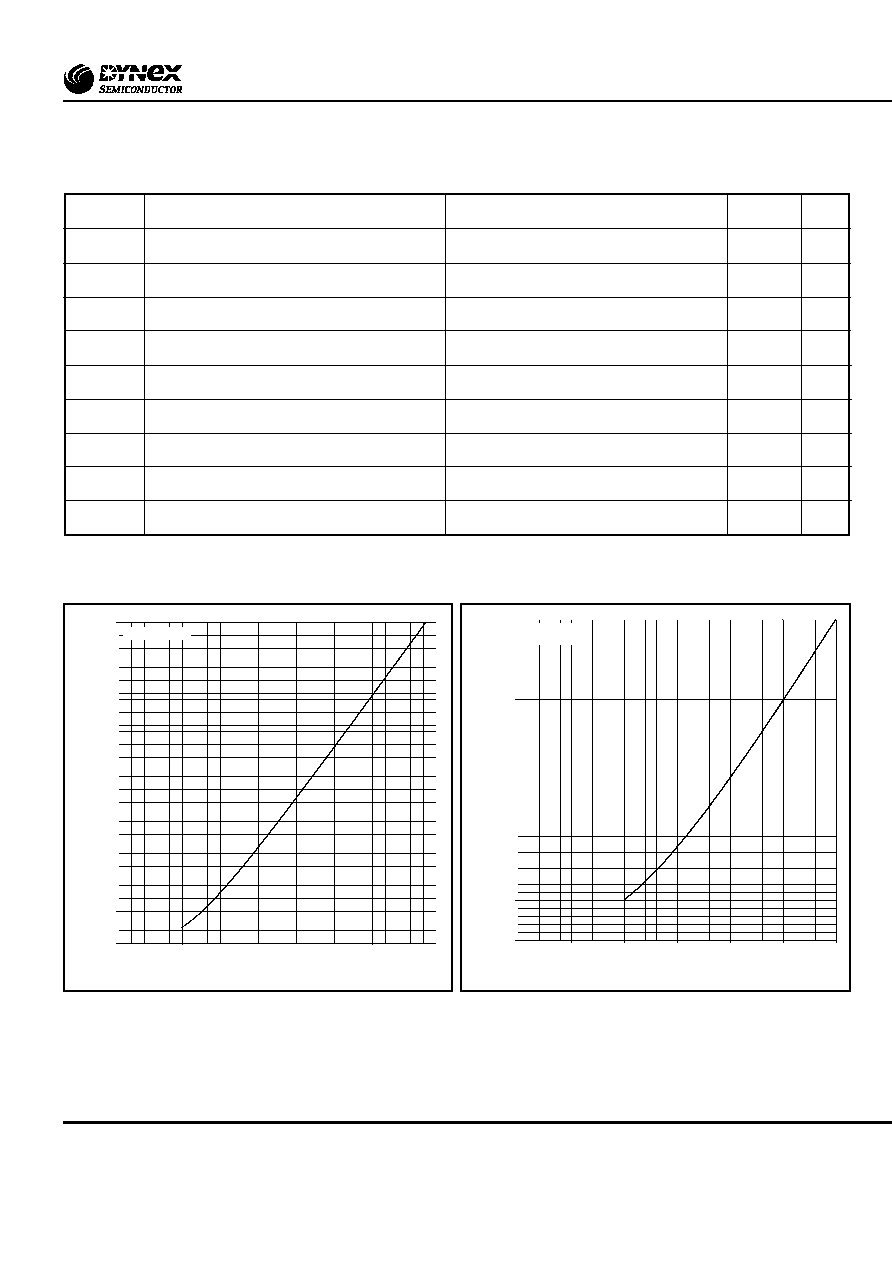
CURVES
Fig.2 Maximum (limit) on-state characteristics
Fig.3 Maximum (limit) on-state characteristics
V
TM
EQUATION
V
TM
= A + Bln (I
T
) + C.I
T
+D.
I
T
Where
A = 0.02866651
B = 0.1590393
C = 1.947584x10
≠4
D = ≠5.23298x10
≠3
these values are valid for T
j
= 125∞C for I
T
500A to 10000A
0.5
1
1.5
2
2.5
3
0
1000
2000
3000
4000
5000
6000
7000
8000
9000
10000
Instantaneous on-state current, I
T
- (A)
Instantaneous on-state voltage, V
T
- (V)
T
j
= 125∞C
0.6
0.8
1.0
1.2
1.4
1.6
0
500
1000
1500
2000
2500
3000
3500
4000
Instantaneous on-state current, I
T
- (A)
Instantaneous on-state voltage, V
T
- (V)
T
j
= 125∞C
1.8