 | –≠–ª–µ–∫—Ç—Ä–æ–Ω–Ω—ã–π –∫–æ–º–ø–æ–Ω–µ–Ω—Ç: DG858DW45 | –°–∫–∞—á–∞—Ç—å:  PDF PDF  ZIP ZIP |

DG858DW45
1/7
FEATURES
q
Double Side Cooling
q
High Reliability In Service
q
High Voltage Capability
q
Fault Protection Without Fuses
q
High Surge Current Capability
q
Turn-off Capability Allows Reduction In Equipment
Size And Weight. Low Noise Emission Reduces
Acoustic Cladding Necessary For Environmental
Requirements
APPLICATIONS
q
Variable speed A.C. motor drive inverters (VSD-AC).
q
Uninterruptable Power Supplies
q
High Voltage Converters.
q
Choppers.
q
Welding.
q
Induction Heating.
q
DC/DC Converters.
KEY PARAMETERS
I
TCM
3000A
V
DRM
4500V
I
T(AV)
1100A
dV
D
/dt
750V/
µ
s
dI
T
/dt
300A/
µ
s
Fig.1 Package outline
Package outline type code : W
See Package Details for further information.
VOLTAGE RATINGS
4500
DG858DW45
Conditions
Type Number
T
vj
= 125
o
C, I
DRM
=100mA,
I
RRM
= 50mA
Repetitive Peak Off-state
Voltage
V
DRM
V
Repetitive Peak Reverse
Voltage
V
RRM
V
16
CURRENT RATINGS
Symbol
Parameter
Conditions
Max.
I
TCM
V
D
= V
DRM
, T
j
= 125
o
C, di
GQ
/dt = 40A/
µ
s,
Cs = 4.0
µ
F, L
S
200nH
A
3000
Units
Repetitive peak controllable on-state current
T
HS
= 80
o
C. Double side cooled, half sine 50Hz.
RMS on-state current
A
A
1100
1720
T
HS
= 80
o
C. Double side cooled, half sine 50Hz.
I
T(RMS)
I
T(AV)
Mean on-state current
DG858DW45
Gate Turn-Off Thyristor
Replaces July 1999 version, DS4334-4.0
DS4334-4.1 May 2000

DG858DW45
2/7
SURGE RATINGS
Conditions
20.0
2.0 x 10
6
kA
A
2
s
Surge (non-repetitive) on-state current
I
2
t for fusing
10ms half sine. T
j
= 125
o
C
10ms half sine. T
j
=125
o
C
di
T
/dt
Critical rate of rise of on-state current
300
20
V/
µ
s
Max.
Units
Rate of rise of off-state voltage
Peak stray inductance in snubber circuit
dV
D
/dt
200
nH
750
V/
µ
s
To 66% V
DRM
; V
RG
= -2V, T
j
= 125
o
C
I
TSM
Symbol
Parameter
I
2
t
V
D
= 3000V, I
T
= 3000A, T
j
=125
o
C
I
FG
> 40A, Rise time < 1.0
µ
s
A/
µ
s
To 66% V
DRM
; R
GK
22
, T
j
= 125
o
C
L
S
I
T
= 3000A, V
D
= V
DRM
, T
j
= 125∞C,
di
GQ
/dt = 40A/
µ
s, Cs = 4.0
µ
F
GATE RATINGS
Symbol
Parameter
Conditions
V
Units
Max.
16
20
Min.
-
20
-
Peak reverse gate voltage
Peak forward gate current
Average forward gate power
Peak reverse gate power
Rate of rise of reverse gate current
Minimum permissable on time
Minimum permissable off time
24
60
-
50
20
-
-
µ
s
100
100
V
RGM
This value maybe exceeded during turn-off
I
FGM
P
FG(AV)
P
RGM
di
GQ
/dt
t
ON(min)
t
OFF(min)
µ
s
A/
µ
s
kW
W
A
THERMAL AND MECHANICAL DATA
Symbol
Parameter
Conditions
Max.
Min.
R
th(c-hs)
Contact thermal resistance
R
th(j-hs)
-
-
0.03
-
0.0021
o
C/W
per contact
Cathode side cooled
Double side cooled
Units
-
0.011
o
C/W
Anode side cooled
o
C/W
0.017
Virtual junction temperature
T
OP
/T
stg
Operating junction/storage temperature range
-
Clamping force
-40
125
44.0
36.0
-40
kN
o
C/W
Clamping force 40kN
With mounting compound
DC thermal resistance - junction to
heatsink surface
T
vj
125
o
C
o
C

DG858DW45
3/7
CHARACTERISTICS
Conditions
Peak reverse current
On-state voltage
V
TM
Peak off-state current
Reverse gate cathode current
50
-
Turn-on energy
Gate trigger current
Delay time
Rise time
Fall time
Gate controlled turn-off time
Turn-off energy
Storage time
Turn-off gate charge
Total turn-off gate charge
Peak reverse gate current
-
12500
V
RGM
= 16V, No gate/cathode resistor
µ
C
I
T
= 3000A, V
DM
= 4200V
Snubber Cap Cs = 4.0
µ
F,
di
GQ
/dt = 40/
µ
s
T
j
= 125
o
C unless stated otherwise
Symbol
Parameter
I
DM
I
RRM
V
GT
Gate trigger voltage
I
GT
I
RGM
E
ON
t
d
t
r
E
OFF
t
gs
t
gf
t
gq
Q
GQ
Q
GQT
I
GQM
Min.
Max.
Units
At 3000A peak, I
G(ON)
= 10A d.c.
-
3.85
V
V
DRM
= 4500V, V
RG
= 2V
-
100
mA
At V
RRM
-
50
mA
V
D
= 24V, I
T
= 100A, T
j
= 25
o
C
-
1.2
V
V
D
= 24V, I
T
= 100A, T
j
= 25
o
C
-
4.0
A
mA
mJ
4400
-
V
D
= 2000V
I
T
= 3000A, dI
T
/dt = 300A/
µ
s
I
FG
= 40A, rise time < 1.0
µ
s
µ
s
2.0
-
-
6.0
µ
s
-
12500
mJ
-
26
µ
s
µ
s
2.5
-
µ
s
28.5
-
-
25000
µ
C
-
950
A
Conditions
Limit
V
dc
= 3500V, T
j
= -40 to + 125∞C,
ambient cosmic radiation at sea level, in
open air, 100% duty cycle.
Units
100
FIT
DC blocking reliability
RELIABILITY

DG858DW45
4/7
CURVES
1.5
2.0
2.5
3.0
3.5
Instantaneous on-state voltage V
TM
- (V)
1000
2000
3000
4000
Instantaneous on-state current I
T
- (A)
Measured under pulse
conditions.
I
G(ON)
= 10A
Half sine wave 10ms
0
4.0
1.0
T
j
= 125∞C
T
j
= 25∞C
Figure 2. On-state characteristics
DG858DW45
5/7
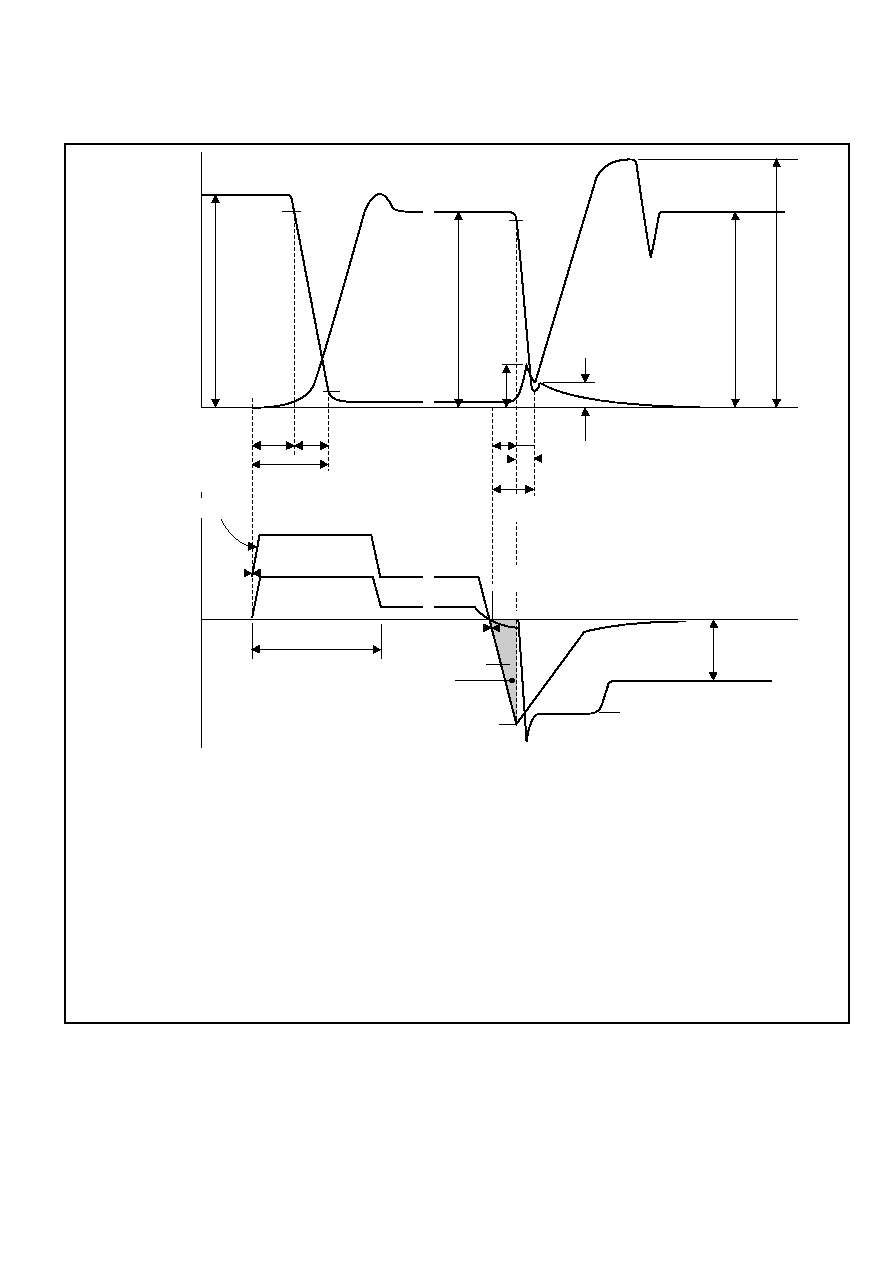
Recommended gate conditions:
I
TCM
= 3000A
I
FG
= 40A
I
G(ON)
= 10A d.c.
t
w1(min)
= 20
µ
s
I
GQM
= 1200A
di
GQ
/dt = 40A/
µ
s
Q
GQ
= 12500
µ
C
V
RG(min)
= 2V
V
RG(max)
= 18V
Anode voltage and current
VD
0.9VD
0.1VD
td
tr
tgt
IT
VDP
0.9IT
ITAIL
dVD/dt
VD VDM
Gate voltage and current
tgs
tgf
tw1
VFG
IFG
0.1IFG
dIFG/dt
0.1IGQ
QGQ
0.5IGQM
IGQM
VRG
V(RG)BR
IG(ON)
tgq
These are recommended Dynex Semiconductor conditions. Other conditions are permitted
according to users gate drive specifications.
Figure 3. General switching waveforms

DG858DW45
6/7
PACKAGE DETAILS
For further package information, please contact your local Customer Service Centre. All dimensions in mm, unless stated
otherwise. DO NOT SCALE.
72 max
ÿ84.6 nom
ÿ84.6 nom
ÿ120 max
27.0
25.5
Cathode
Anode
Gate connector ÿ3.0
Auxiliary cathode connector ÿ3.0
12∞
2 holes ÿ3.6 x 2.0 deep (One in each electrode)
Nominal weight: 1700g
Package outline type code: W
Associated Literature/Products
Publication No.
Title/Part Number
AN4571
Application note - GDU9X-XXXXX Series GTO gate drive units.
DS4567
GDU90-20721 GTO gate drive unit.
DS4568
GDU90-20722 GTO gate drive unit.
DS4150
DSF8045SK - Snubber diode.
DS4153
DSF21545SV - Antiparallel/freewheel diode.

DG858DW45
7/7
CUSTOMER SERVICE CENTRES
Central Europe Tel: +33 (0)1 69 18 90 00. Fax: +33 (0)1 64 46 54 50.
North America Tel: 011-800-5554-5554. Fax: 011-800-5444-5444.
UK, Scandinavia & Rest Of World Tel: +44 (0)1522 500500. Fax: +44 (0)1522 500020.
SALES OFFICES
Central Europe Tel: +33 (0)1 69 18 90 00. Fax: +33 (0)1 64 46 54 50.
North America Tel: (613) 723-7035. Fax: (613) 723-1518. Toll Free: 1.888.33.DYNEX (39639) /
Tel: (831) 440-1988. Fax: (831) 440-1989 / Tel: (949) 733-3005. Fax: (949) 733-2986.
UK, Scandinavia & Rest Of World Tel: +44 (0)1522 500500. Fax: +44 (0)1522 500020.
These offices are supported by Representatives and Distributors in many countries world-wide.
© Dynex Semiconductor 2000 Publication No. DS4334-1 Issue No.4.1 May 2000
TECHNICAL DOCUMENTATION ≠ NOT FOR RESALE. PRINTED IN UNITED KINGDOM
HEADQUARTERS OPERATIONS
DYNEX SEMICONDUCTOR LTD
Doddington Road, Lincoln.
Lincolnshire. LN6 3LF. United Kingdom.
Tel: 00-44-(0)1522-500500
Fax: 00-44-(0)1522-500550
DYNEX POWER INC.
Unit 7 - 58 Antares Drive,
Nepean, Ontario, Canada K2E 7W6.
Tel: 613.723.7035
Fax: 613.723.1518
Toll Free: 1.888.33.DYNEX (39639)
This publication is issued to provide information only which (unless agreed by the Company in writing) may not be used, applied or reproduced for any purpose nor form part of any order or contract nor to be regarded as
a representation relating to the products or services concerned. No warranty or guarantee express or implied is made regarding the capability, performance or suitability of any product or service. The Company reserves
the right to alter without prior notice the specification, design or price of any product or service. Information concerning possible methods of use is provided as a guide only and does not constitute any guarantee that such
methods of use will be satisfactory in a specific piece of equipment. It is the user's responsibility to fully determine the performance and suitability of any equipment using such information and to ensure that any publication
or data used is up to date and has not been superseded. These products are not suitable for use in any medical products whose failure to perform may result in significant injury
or death to the user. All products and materials are sold and services provided subject to the Company's conditions of sale, which are available on request.
All brand names and product names used in this publication are trademarks, registered trademarks or trade names of their respective owners.
http://www.dynexsemi.com
e-mail: power_solutions@dynexsemi.com
Datasheet Annotations:
Dynex Semiconductor annotate datasheets in the top right hard corner of the front page, to indicate product status. The annotations are as follows:-
Target Information: This is the most tentative form of information and represents a very preliminary specification. No actual design work on the product has been started.
Preliminary Information: The product is in design and development. The datasheet represents the product as it is understood but details may change.
Advance Information: The product design is complete and final characterisation for volume production is well in hand.
No Annotation: The product parameters are fixed and the product is available to datasheet specification.