 | –≠–ª–µ–∫—Ç—Ä–æ–Ω–Ω—ã–π –∫–æ–º–ø–æ–Ω–µ–Ω—Ç: MAS281 | –°–∫–∞—á–∞—Ç—å:  PDF PDF  ZIP ZIP |
MAS281
1/55
The MAS281 Microprocessor is a MIL-STD-1750A (Notice
1), 16-bit Central Processing Unit (CPU). It consists of three
CMOS/SOS large-scale integration (LSI) chips: the MA17501
Execution Unit (EU), the MA17502 Control Unit (CU), and the
MA17503 Interrupt Unit (IU). These three units can be
mounted on, and interconnected within a 64-pin ceramic
substrate. The microprocessor is also available as a 3-chip set
without the ceramic substrate (see ordering information on
page 55).
The MAS281 is optimised for real-time l/O and arithmetic
intensive operations. Key performance-enhancing features
include a parallel multiplier/accumulator, 32-bit barrel shifter,
instruction pre-fetch queue, and multiport register file.
Additional features include a comprehensive Built-ln-Test
(BIT), interval timers A and B, trigger-go counter, and Start-Up
ROM interface.
In accordance with MIL-STD-1750A, the MAS281
supports a 64K-word address space. An optional BMA31751
Memory Management Unit/Block Protect Unit (MMU(BPU))
chip may be added externally to expand this address space to
1M-words or add a 1K-word memory block protection
capability,
The MAS281 is offered in several screening grades which
are described in this document. For availability of speed
grades, please contact Dynex Semiconductor.
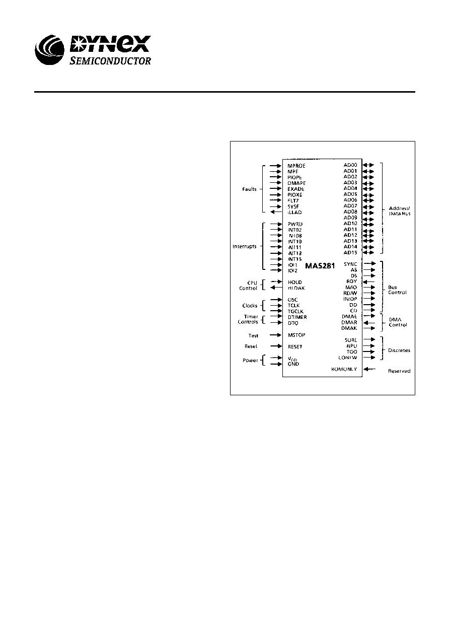
BLOCK DIAGRAM
FEATURES
s
MIL-STD-1750A 16-Bit Microprocessor
s
Full Performance over Military Temperature Range
(-55
∞
C to + 125
∞
C)
s
Radiation Hard CMOS/SOS Technology
s
Performance Optimised Architecture
- Parallel Multiplier/Accumulator
- 32-bit Barrel Shifter
- Instruction Pre-Fetch
- Multi-Port Register File
s
Implements MlL-STD-1750AOptions
- Timers A and B
- Trigger-Go Counter
- Start-Up ROM Interface
s
64 K-word Address Space Expandable to 1 M-word with
Optional MMU
MAS281
MIL-STD-1750A Microprocessor
Replaces June 1999 version, DS3563-4.0
DS3563-5.0 January 2000
MAS281
2/55
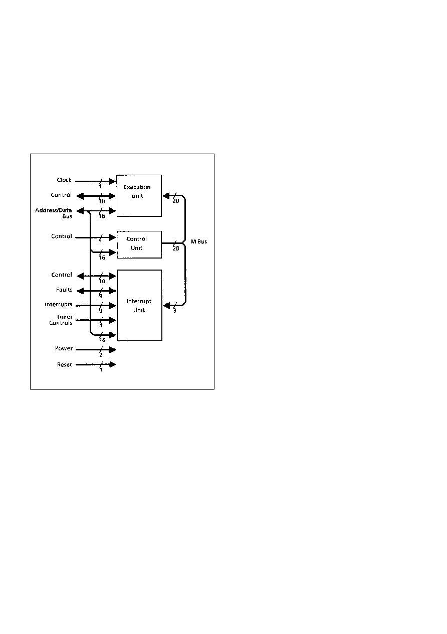
1.0 ARCHITECTURE
The MAS281 Microprocessor is a high performance
implementation of the MIL-STD-1750A (Notice 1) instruction
set architecture. It consists of three custom CMOS/SOS Large
Scale Integration chips referred to as the Execution Unit,
Control Unit, and Interrupt Unit - mounted on, and
interconnected within, a 64-pin, dual in-line ceramic substrate.
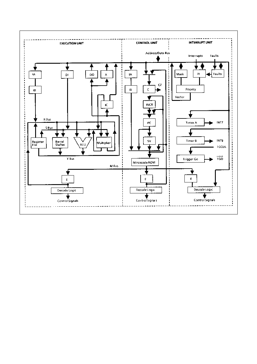
Figure 1 depicts the interconnection of these chips via the
substrate while Figure 2 depicts the architectural details within
each chip.
The MAS281 architecture has been optimised for both real
time l/O and arithmetic intensive operations. Two key features
of this architecture which contribute to the overall high
performance of the MAS281 are; a barrel shifter and a parallel
multiplier/accumulator. These subsystems allow the MAS281
to perform multi-bit shifts, multiplications, divisions, and
normalisations in a fraction of the clock cycles required on
machines not having such resources. This is especially true of
floating-point operations, in which the MAS281 excels. Such
operations constitute 16% of the Digital Avionics Instruction
Set (DAIS) mix and a generally much higher percentage of
many signal processing algorithms, therefore having a
significant impact on system performance.
In accordance with MIL-STD-1750A, the MAS281 can
access a 64K-word address space. With the addition of an
external MA31751 chip configured as a Memory Management
Unit (MMU), this address space may be expanded to a full
1Mword. Furthermore, this configuration provides write and
access lock and key protection down to 4K-word blocks. By
also configuring the MA31751 as a Block Protect Unit (BPU),
write protection may be extended down to 1K-word blocks. For
those applications not requiring adherence to the address
space requirements of MIL-STD-1750A, the MAS281 may be
optionally configured with up to 1Mword each of instruction
and operand space.
In addition to implementing all of the required features of
MIL-STD-1750A, the MAS281 also incorporates a number of
optional features. Interval timers A and B as well as a trigger-
go counter are provided. Most specified XIO commands are
decoded directly on the module and an additional set of
commands, associated with MMU and BPU operations, are
directly decoded on the MA31751 chip. Those commands not
directly decoded are output for decoding by external logic in
accordance with the XIO and VIO protocols of MIL-STD-
1750A.
1.1 EXECUTION UNIT (EU)
The EU provides the computational resources for the
MAS281. Key features include: (1) a three-bus (R, S, and Y)
data path consisting of an arithmetic/logic unit (ALU), three-
port register file, barrel shifter, parallel multiplier/accumulator,
and status register; (2) instruction fetch registers IC, IA, and IB;
(3) operand transfer registers A, Dl, and DO; (4) a state
sequencer; and (5) microinstruction decode logic. A brief
description of these features follows:
1.1.1 ARITHMETIC/LOGIC UNIT (ALU)
A full function 16-bit ALU is used to perform arithmetic and
logic operations on one or two 16-bit operands in a single
machine cycle. The ALU supports 16-bit fixed-point single-
precision, 32-bit fixed-point double-precision, 32-bit floating-
point, and 48-bit floating-point extended precision data in two's
complement form. The ALU generates several machine flags
which reflect the outcome of its operations. These flags are
stored in the condition status (CS) field of the status register.
1.1.2 THREE PORT REGISTER FILE
A 24-word by 16-bit wide register file is used to store
operands, addresses, base pointers, stack pointers, indexes,
and temporary values. Registers R0 through R15 are general
purpose and user accessible in accordance with MIL-STD-
1750A; remaining registers are accessible only by microcode.
Wrap-around concatenation of R0 through R15 allows 32- and
48-bit operands to be stored. The three-port architecture
allows two 16-bit operands to be read and a third 16-bit
operand to be written simultaneously.
Figure 1: MAS281 Microprocessor Block Diagram
MAS281
3/55
Figure 2: MAS281 Architecture
1.1.3 PARALLEL MULTIPLIER/ACCUMULATOR
This multiplies a 24-bit multiplicand by a 4-bit multiplier and
accumulates the product in a single machine cycle. Only four
iterations through the multiplier are required to complete a 16-
bit by 16-bit multiply.
1.1.4 BARREL SHIFTER
This shifter is a 32-bit input, 16-bit output right-shift
network. The barrel shifter allows multibit shifts to be
accomplished in a single machine cycle and is used by the
microcode for all shift, rotate, and normalise operations.
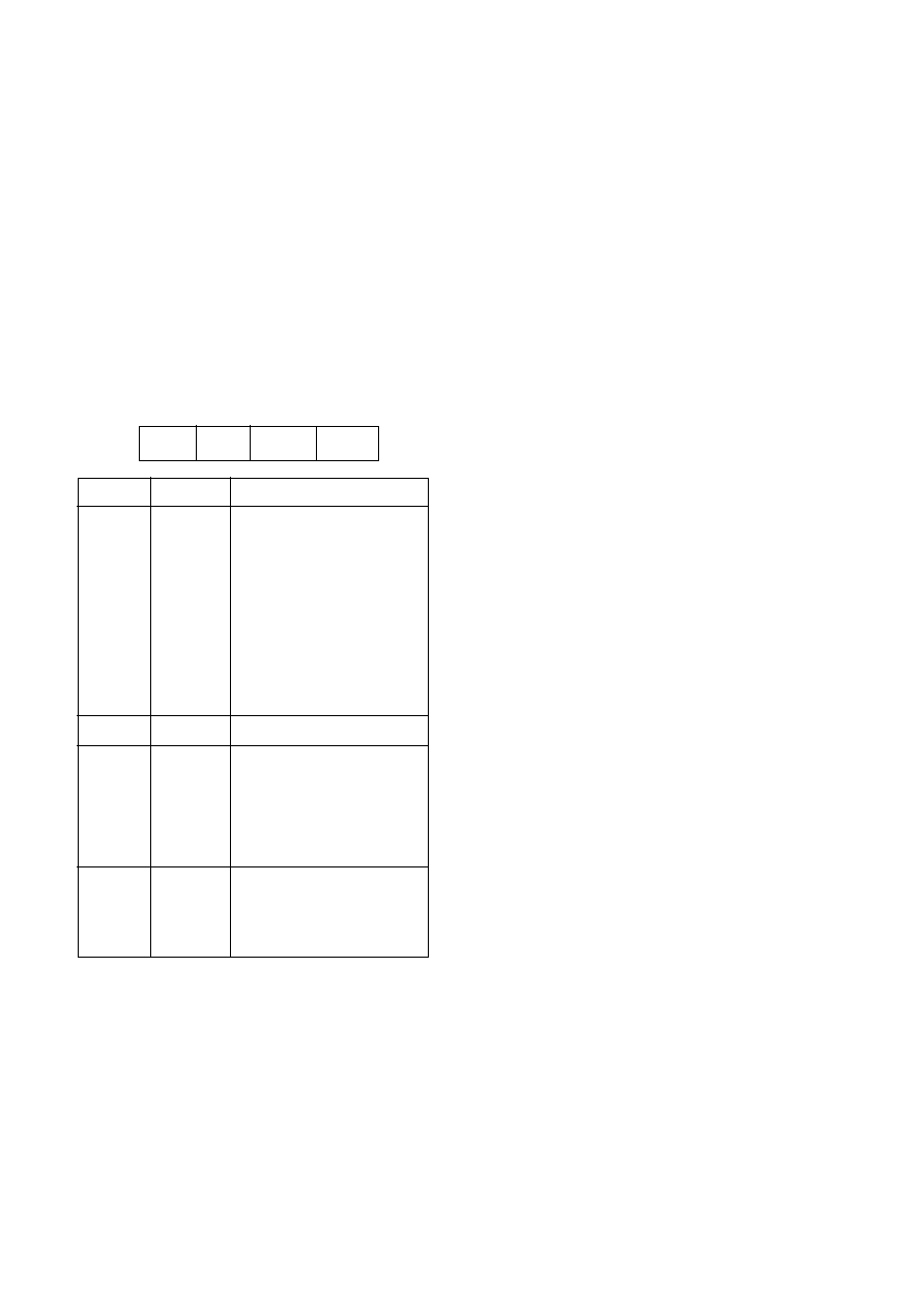
1.1.5 STATUS REGISTER
This 16-bit register holds the condition status (CS) bits C,
P, Z, and N; the 4-bit address state (AS) field; and the 4bit
processor state (PS) field. The CS bits are updated after each
logical, shift, and arithmetic operation performed by the ALU.
The CU interrogates these bits during conditional
operations to determine which course of action to follow. The
AS field is used during expanded memory access to define the
page register set to be used for instruction and operand
memory references. The PS field is used during memory
protect operations to define the access key used for memory
accesses. The PS field is also used during execution of
privileged instructions. PS must be zero for such operations to
be legal. Figure 3 depicts the status register format
1.1.6 STATE SEQUENCER
The EU utilises a state machine, clocked by the system
oscillator, to generate processor timing and control signals.
These signals constitute the lowest level of control available
within the module, and provide the framework for basic
operations, such as selecting the next microinstruction to be
executed, sequencing bus control signals to effect a memory
transfer, or performing an operation within the ALU. Each
complete pass through the state machine corresponds to one
such operation and constitutes a machine cycle.
MAS281
4/55
1.1.7 OPERAND TRANSFER REGISTERS
The Address (A), Data In (Dl), and Data Out (DO) registers
serve to buffer transfers between the data path and the
Address/Data (AD) bus. These registers are used under
microcode control and are not directly accessible by software.
A description of the use of these registers during memory and
l/O operations is provided in section 3.0.
1.1.8 INSTRUCTION FETCH REGISTERS
The Instruction Counter (IC), Instruction A (IA), and
Instruction B (IB) registers allow sequential instruction fetches
to be performed without the assistance of the ALU. The IC
register, which holds a 16-bit address and points to the next
instruction to be fetched, is loaded indirectly via reset, jump, or
branch operations. Once loaded, it uses a dedicated counter to
sequence from one instruction to the next. IA and IB serve as
an instruction pipeline with IA storing the next instruction to be
executed. Dl also plays a role by storing any immediate
operands. Use of these registers during instruction fetches is
described in section 3.0.
1.1.9 MICROCODE CONTROL LOGIC
All EU operations are performed under microcode control.
As depicted in Figure 2, microinstructions are provided by the
CU over the M bus, buffered by the Execution (E) register, and
decoded to generate various control signals.
1.2 CONTROL UNIT (CU)
The CU provides microprogrammed control of all MAS281
operations. It features a microsequencer, a microcode storage
ROM, and an instruction mapping ROM. A brief description of
these features follows:
1.2.1 MICROSEQUENCER
This 12-bit wide microcode address generator controls all
microcode ROM accesses. The microsequencer features a
program counter (PC) which points to the next sequential
microinstruction, a program counter save register (SV) to save
return addresses for microsubroutines, address increment
logic (INCR), instruction pipeline registers (IA and IB), a next
address multiplexer, a loop counter (C), and various
miscellaneous systems.
The microsequencer controls the execution of each
MILSTD-1750A, or macro, instruction by stepping through its
corresponding microcode sequence. If the macroinstruction is
a conditional, the CS bits of the status word will be interrogated
to determine the necessary course of action. At the completion
of each macroinstruction, the microsequencer checks to see if
a Hold request or an interrupt is pending. If so, the
microsequencer will branch to the appropriate microinstruction
sequence. If not, the microsequencer begins sequencing the
next macroinstruction.
Note that the microsequencer is itself under the control of
the EU state sequencer. Each processor machine cycle
corresponds to the execution of a single microinstruction.
A machine cycle requires five or more oscillator cycles
with the exact number determined by the type of operation
being performed. Internal processor operations, excluding
internally decoded XIO commands, require either five or six
oscillator cycles, the former associated with sequential
microcode execution and the latter with microcode branches.
Internally decoded XIO commands require a minimum of six
oscillator cycles to complete. External processor operations
require a minimum of five oscillator cycles to complete.
The internal ready signal is generated by the IU whenever
an internally decoded XIO command is detected An external
ready interface is provided which allows external machine
cycles to be extended when interfacing with slow devices. The
external ready signal is provided by external logic and must be
asserted in order to conclude the machine cycle.
Field
Bits
Description
CS
CONDITION STATUS:
0
C-
Carry from an
addition or no borrow from
a subtraction
1
P-
Result >0
2
Z-
Result = 0
3
N-
Result<0
R
4 - 7
RESERVED
PS
8 - 11
PROCESSOR STATE:
(a)- Memory access key
code
(b)- Privileged instruction
enable
AS
12 - 15
ADDRESS STATE:
Page register sets for
expanded memory
addressing
Figure 3: Status Word Format
CS
R
PS
AS
3 4
7 8
11 12
15
0

MAS281
5/55
or more faults in FT will cause a level 1 (machine error)
interrupt request. Once a fault is set in FT, it may only be
cleared via an XIO command.
1.3.5 TIMERS A AND B
These are two 16-bit software controllable timers. Timer A
is clocked by the TCLK input while Timer B is clocked by the
internally generated TCLK/10. Timers A and B will generate
interrupt levels 7 and 9, respectively, when their maximum
counts of 65,536 are reached.
1.3.6 TRIGGER-GO COUNTER
This 16-bit counter is clocked by the TGCLK input, is
enabled during system initialisation, and may be reset but not
stopped by software action. It is stopped, however, upon
overflow or by assertion of the DTIMERN input. Upon overflow,
the TGON discrete output goes low and stays low until the
counter is reset by software. This counter is typically used as a
system "watchdog" timer.
1.3.7 XIO COMMAND DECODE LOGIC
This logic decodes all internally supported XlO commands
and generates the control signals necessary to carry out the
commanded action. An internal ready signal is generated upon
command detection and is used by the EU state sequencer as
previously discussed. Table 7b in Section 4.0 identifies the XlO
commands which are internally supported by the MAS281.
1.3.8 MICROCODE CONTROL LOGIC
Decode logic, which translates microcode received from
the CU into control signals, is used both by the MAS281 and by
the external system.
2.0 INTERFACE SIGNALS
2.1 PIN ASSIGNMENTS
Figure 4 defines the pin assignment for the MAS281
module. See section 10.0 for full packaging and pin
assignment information.
All signals - with the exception of power, ground and
ROMONLYN - are TTL compatible. In addition, each function
is provided with Electrostatic Discharge (ESD) protection
circuitry. Figure 5 depicts a typical system implementation
using many of these signals. Throughout this data sheet,
active low signals are denoted either by placing a bar over the
signal name, or by following the signal name with an "N" suffix,
e.g., DDN. If a signal has a dual function, both function names
will be used separated by a "/". The function name to the left of
the "/" will be active high while the function to the right will be
active low, again with an "N" suffix, e g., RD/WN.
1.2.2 MICROCODE ROM
This is a 2k- (2048) word by 40-bits/word ROM which
stores the microinstructions that implement the MIL-STD-
1750A instruction set. The address of the next microinstruction
to be accessed is generated by the microsequencer. The
accessed microinstruction is output to the M-bus and
broadcast to the EU and IU. In addition to the microinstruction
sequences corresponding to the MIL-STD-1750A instructions,
the microcode ROM also stores sequences for performing
initialisation, interrupt response, Hold response, instruction
prefetch, built-intest (BIT), and BlFs.
1.2.3 INSTRUCTION MAPPING ROM
This is a 512-word by 8-bits/word ROM which is used
during microcode branches.
1.3 INTERRUPT UNIT (IU)
The IU incorporates a pending interrupt register, a mask
register, a priority encoder, a fault register, two interval timers
(A and B), a trigger-go counter, XIO command decode logic,
and microcode control logic. A brief description of these
features follows:
1.3.1 PENDING INTERRUPT REGISTER (PL)
This 16-bit register is used to capture and hold interrupts
until they can be processed by software. Pl supports three
dedicated external, six user-definable external, and seven
dedicated internal interrupts. Interrupts are captured at the
beginning of each machine cycle and are stored using a logic 1
to represent a pending interrupt. Anti-repeat logic is provided
to prevent multiple captures of the same interrupt.
1.3.2 MASK REGISTER (MK)
This 16-bit register is used to store the interrupt mask.
Interrupts are masked by ANDing each mask bit with its
corresponding Pl register bit. Interrupts which are masked will
be captured in the Pl register but will not be acted on until
unmasked. Interrupt level 0 can not be masked. A logic 0 in a
given bit position indicates that the corresponding bit in the Pl
register will be masked.
1.3.3 PRIORITY ENCODER
This encoder generates an interrupt request to the CU
whenever one or more unmasked interrupts are pending and
enabled in the Pl and encodes the highest priority unmasked
pending interrupt as a 4-bit vector. This vector is read by the
EU over the AD bus during interrupt servicing in order to create
the interrupt Linkage and Service pointers.
1.3.4 FAULT REGISTER
This 16-bit register is used to capture and hold both internal
and user implemented external faults. Faults are captured at
the beginning of each machine cycle and are stored using
positive logic, i e, a logic "1" represents a fault. Setting any one