 | –≠–ª–µ–∫—Ç—Ä–æ–Ω–Ω—ã–π –∫–æ–º–ø–æ–Ω–µ–Ω—Ç: EDE-1144 | –°–∫–∞—á–∞—Ç—å:  PDF PDF  ZIP ZIP |
Copyright
©
1999 E-Lab Digital Engineering, Inc. All Rights Reserved.
Page 1/7
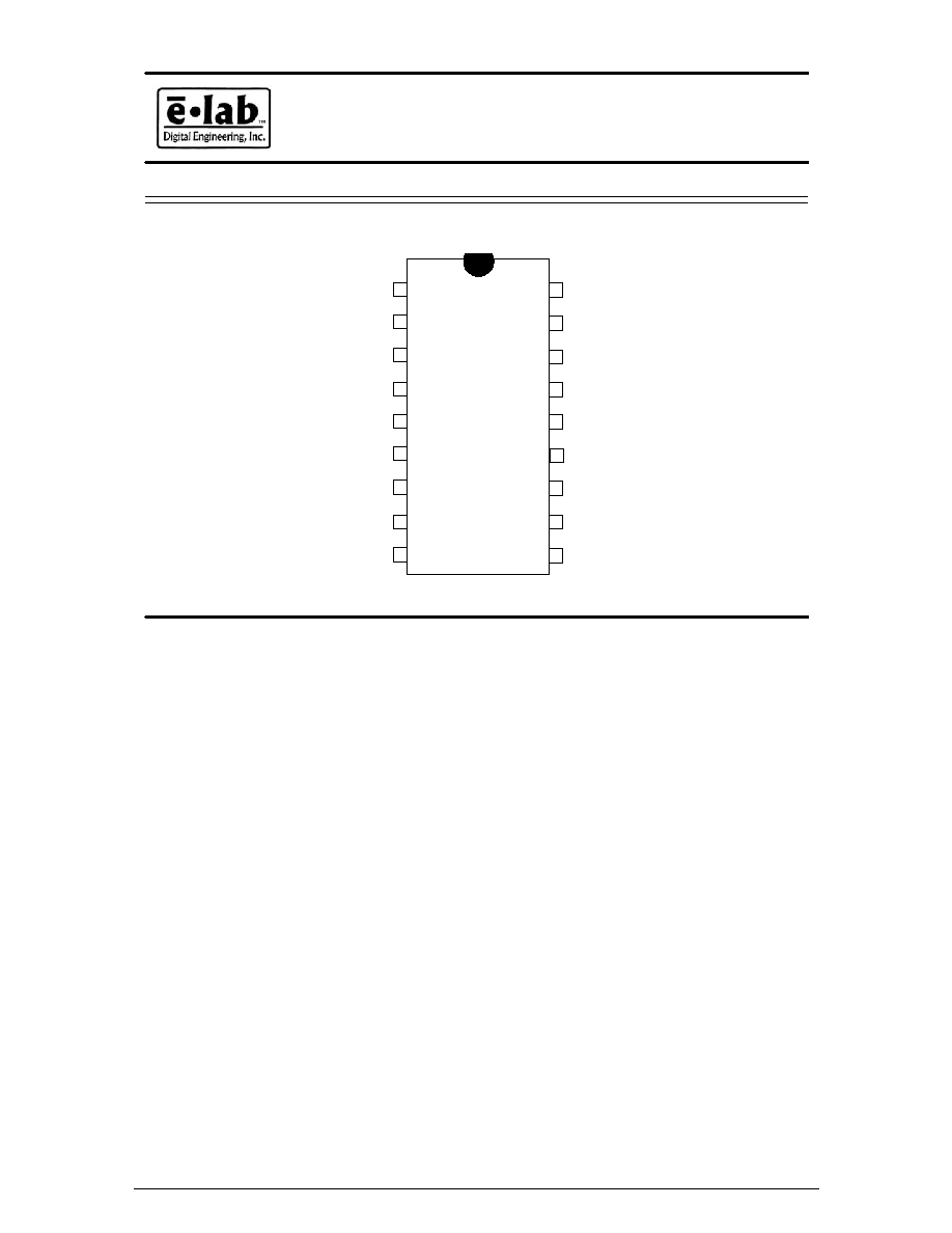
EDE1144 Keypad Encoder IC
4 x 4 Matrix Keypad Encoder IC
RS-232 Output 1
0=2400, 1=9600 Baud 2
Connect to +5V 3
Connect to +5V 4
Digital Ground 5
Row 0 Output 6
Row 1 Output 7
Row 2 Output 8
Row 3 Output 9
18 Beeper Output
17 Data Valid Output
16 Oscillator Conection
15 Oscillator Connection
14 Connect to +5V
13 Column 3 Input
12 Column 2 Input
11 Column 1 Input
10 Column 0 Input
XMIT
Baud
+5V
+5V
GND
R0
R1
R2
R3
Beep
Valid
OSC1
OSC2
+5V
C3
C2
C1
C0
EDE1144
Functionality & Feature Set:
∑
Automatic key repeat after delay
∑
Contact debouncing
∑
Keybeep provides tactile feedback to operator
∑
Electrically quiet (reduced EMI) keypad scanning
∑
Serial / Parallel outputs available
∑
Data Valid output signal for interrupt activation
∑
2400/ 9600 serial Baud rates
∑
Available in 18 pin DIP or SOIC packages
∑
Interfaces to any microcontroller or microprocessor
∑
Cost effective for OEM applications
The EDE1144 Keypad Encoder IC is designed to interface a matrix-type 4 row x 4 column (16 key
or less) keypad to a microcontroller or other host processor. A one-wire serial or four-wire
parallel interface returns the keypress data and can be used in conjunction with a 'data valid'
signal for polled or interrupt-driven applications. The EDE1144 provides enhanced keypad
features such as contact debouncing and key auto-repeat in an easy-to-use package that will lower
software overhead in the host microcontroller and reduce the I/O pin requirements from eight to
one, frequently resulting in the use of a less costly host microcontroller in your design.
In addition, the EDE1144 is electrically quiet. Many keypad encoders continually scan the
keypad, radiating EMI noise from the wires leading to the keypad (resulting in trouble during
emissions testing & final product certification & approval). The EDE1144 reduces this problem by
monitoring the keypad with unchanging signals, and then scanning only once each time a
keypress is detected.

EDE1144 Keypad Encoder IC
Page 2/7
PIN DEFINITIONS
Keypad Connection Pins:
(R0) Row 0 / Data 0 Output (Pin 6)........................................Multiplexed Keypad Row 0,
Host System Data Input 0
(R1) Row 1 / Data 1 Output (Pin 7)........................................Multiplexed Keypad Row 1,
Host System Data Input 1
(R2) Row 2 / Data 2 Output (Pin 8)........................................Multiplexed Keypad Row 2,
Host System Data Input 2
(R3) Row 3 / Data 3 Output (Pin 9)........................................Multiplexed Keypad Row 3,
Host System Data Input 3
(C0) Column 0 Input (Pin 10).................................................Multiplexed Keypad Column 0
(through 330 resistor)
(C1) Column 1 Input (Pin 11).................................................Multiplexed Keypad Column 1
(through 330 resistor)
(C2) Column 2 Input (Pin 12).................................................Multiplexed Keypad Column 2
(through 330 resistor)
(C3) Column 3 Input (Pin 13).................................................Multiplexed Keypad Column 3
(through 330 resistor)
Control & Data Pins:
Baud (Pin 2)...........................................................................Baud Rate Selection;
0=2400, 1=9600
XMIT (Pin 1)..........................................................................Serial Data Output (N-8-1);
RS232 (TTL/CMOS Voltages)
Valid (Pin 17).........................................................................Data Valid Signal / Interrupt:
Parallel data valid when low
Beep (Pin 18)..........................................................................Modulated Output Signal:
Oscillates on keypress or repeat
Clock / Power Pins:
OSC1 (Pin 16)........................................................................One pin of 4MHz parallel-cut
crystal or resonator, or a direct
TTL clock input
OSC2 (Pin 17)........................................................................Other pin of 4MHz parallel-cut
crystal or resonator, or leave
floating if OSC1 driven with
a TTL clock input
+5V (Pins 3,4,14)..................................................................Connect to +5V DC
GND (Pin 5)...........................................................................Connect to 0V DC (Ground)
Note: DIP are SOIC (surface mount) packages of the EDE1144 have identical pinout and
pincount. Please specify EDE1144/P (DIP) or EDE1144/SO (SOIC) when ordering.

EDE1144 Keypad Encoder IC
Page 3/7
0
4
8
12
1
5
9
13
2
6
10
14
3
7
11
15
Beeper
Output
D0
D1
D2
D3
Data
Valid
Data Output
Row 1
Row 2
Row 3
Row 0
Column 3
Column 2
Column 1
Column 0
Serial
Output
2400 / 9600 Baud Select Input
4x4 Multiplexed Keypad
EDE1144
Keypad
Encoder
Figure One: Connection Block Diagram
As illustrated by Figure One, the EDE1144 resides between the keypad and host microcontroller/
processor. The host microcontroller receives keypress data via either the four parallel data
outputs (D0-D3, Pins 6-9) or the Serial Data Output (Pin 1). The Data Valid signal (Pin 17) is
activated upon keypress (and upon each key repeat cycle if key is held). The Data Valid signal is
activated prior to transmission of the serial data to allow polled (software-UART) style host serial
systems such as the BASIC StampTM or a microcontroller without a hardware UART to enter the
serial receive routine and receive the keypress data without needing to continually wait for the
start bit. Note that the data outputs to the host microcontroller reside on the row output pins
(Pins 6-9), therefore parallel-output data should only be read while the Data Valid (Pin 17) signal
is active (low). Upon powerup, the four data output pins will be high, and will remain high
except when a key is pressed.
The following table illustrates the data values returned by the serial and parallel outputs of the
EDE144 upon each keypress. Note that the serial values are increased (by Hexadecimal 30 ($30)
for 0-9 and Hex $37 for 10-15) to correspond to the ASCII equivalent (0-9,A-F) of the BCD
(binary-coded decimal) value on the parallel outputs.
Key:
0
1
2
3
4
5
6
7
RS-232:
$30
('0')
$31
('1')
$32
('2')
$33
('3')
$34
('4')
$35
('5')
$36
('6')
$37
('7')
D3..D0:
0000
0001
0010
0011
0100
0101
0110
0111
Key:
8
9
10
11
12
13
14
15
RS-232:
$38
('8')
$39
('9')
$41
('A')
$42
('B')
$43
('C')
$44
('D')
$45
('E')
$46
('F')
D3..D0:
1000
1001
1010
1011
1100
1101
1110
1111
Table One: Keynumber vs. Output Data

EDE1144 Keypad Encoder IC
Page 4/7
OVERVIEW OF OPERATION
Table One of the previous page illustrates the data that is output upon each keypress. The
following sequence is initiated upon each keypress, and is repeated if the key is held:
1. Keypress is detected
2. One scan cycle is performed
3. Parallel Outputs (D3..D0) are latched with the appropriate value
4. Data Valid signal is activated (pulled low)
5. Beeper (1KHz square wave) is activated for 45mS
6. Serial data is transmitted
This entire cycle takes 50mS (regardless of Baud rate selected). If a key is held longer than the
autorepeat delay of 660 mS, the cycle is repeated again at a rate of 5 times per second. The
following timing diagram illustrates the above sequence:
0ms
10ms
20ms
30ms
40ms
50ms
Keypress
Parallel_Outputs
Data_Valid_Output
Serial_Output
Beeper_Output
D3..D0 latched with appropriate value
45mS
50mS
1uS
(Multiple transitions are due to contact bounce)
(Square wave is not to scale)
Once a key is pressed, any additional closures (bounce) of that contact, or of any other contacts
are ignored for 50mS, during which several signals are output by the EDE1144. First, the parallel
outputs D0..D3 (Pins 6-9) are latched with the appropriate keypress value. One microsecond
later, the Data Valid Output (Pin 17) goes low, indicating that there is valid data on the parallel
output pins. Following this, the Beeper Output (Pin 18) pulse stream is generated for 45mS,
providing auditory confirmation to the keypad operator that a key has been pressed. Finally, the
RS-232 Output (Pin 1) transmits the keypress data at the Baud rate selected by the Baud rate input
select (Pin 2). After this, a variable (determined by Baud rate chosen) delay period is waited to
make the entire process to last precisely 50mS.
If a key is held longer that the autorepeat delay of 660mS, the outputs are cleared and this entire
process is repeated every 204mS until the key is released by the operator.

EDE1144 Keypad Encoder IC
Page 5/7
XMIT
Baud
+5V
+5V
GND
R0
R1
R2
R3
Beep
Valid
OSC1
OSC2
+5V
C3
C2
C1
C0
EDE1144
+5V
+5V
Beeper
4 x 4 Keypad
D0 (LSB)
D1
D2
D3 (MSB)
4.7K Ohm
330 Ohm
Serial Output
Data Valid / Interrupt Output
1K Ohm
4 MHz
Parallel Outputs
Figure Two: Schematic of Keypad Connection
Figure Two illustrates a typical connection of a 4x4 keypad to the EDE1144. Note that R0-R3
(Pins 6-9) are connected to the keypad rows through 330 Ohm resistors. They are present to
prevent a short circuit during the scan cycle in case more that one key is being held at a time, and
they can also help to lower radiated emissions from the keypad wires. The 4.7K Ohm resistors on
the keypad columns are pulldowns to prevent the EDE1144 column inputs from floating or
oscillating. Pulldowns should be present on all four column inputs (C0..C3) regardless of the
keypad size or configuration being used. Note: Power and Ground connections have been
omitted from the EDE1144 hookup shown in Figure Two to simplify the illustration. They must
be connected in actual operation. Also, when using a 4MHz resonator with internal capacitors,
the third (center) pin should be connected to ground.
PARALLEL DATA CONNECTION
To read data from the EDE1144 in a parallel format the host microcontroller will input from the
four data inputs D0,D1,D2, & D3, which also serve as the row drive signal pins R0,R1,R2, & R3
(see Figure Two). While the EDE1144 is waiting for a keypress, it will hold these lines at 1111
(all high). Once a key is pressed, the data output pins will toggle while the keypad is scanned so
that the EDE1144 can determine which key was pressed. Then, the appropriate data value (see
Table One) will be output onto the data outputs (via the row output pins), and the Data Valid
Output (Pin 17) will go low. This pin will stay low for 50 mS, during which the Data Output pins
will hold the keypress data. The keypress data should be sampled during this 50mS window.
Both the Parallel & Serial Data outputs are activated on each keypress (and autorepeat cycle);
designers using the parallel data outputs can ignore the serial data output (and vice versa -
designers using the serial data output can ignore the parallel data output).