 | –≠–ª–µ–∫—Ç—Ä–æ–Ω–Ω—ã–π –∫–æ–º–ø–æ–Ω–µ–Ω—Ç: 8508701ZX | –°–∫–∞—á–∞—Ç—å:  PDF PDF  ZIP ZIP |

ELH0041G8838508701ZX
September
1992
Rev
G
ELH0041G 883 8508701ZX
0 1 Amp Power Operational Amplifier
Note All information contained in this data sheet has been carefully checked and is believed to be accurate as of the date of publication however this data sheet cannot be a ``controlled document'' Current revisions if any to these
specifications are maintained at the factory and are available upon your request We recommend checking the revision level before finalization of your design documentation Patent pending
1989 Elantec Inc
Features
High output current
200 mA
Excellent open-loop
gain
106 dB
Low offset voltage
1 mV
Wide full power
bandwidth
20 kHz
High slew rate
3 V
ms
MIL-STD-883 devices 100%
manufactured in U S A
Ordering Information
Part No
Temp Range Pkg Outline
ELH0041G 883B b55 C to a125 C TO-8 MDP002
8508701ZX is the SMD version of this device
Connection Diagram
0041 ≠ 1
Top View
General Description
The ELH0041 are general purpose operational amplifiers capa-
ble of delivering large output currents not usually associated
with conventional IC op amps the ELH0041 delivers currents
of 200 mA at voltage levels closely approaching the available
power supplies In addition both the inputs and outputs are
protected against overload These devices are compensated with
a single external capacitor and are free of any unusual oscilla-
tion or latch-up problems
For applications requiring output currents in excess of 1A see
the ELH0021 data sheet
The excellent input characteristics and high output capability
of the ELH0041 make it an ideal choice for power applications
such as DC servos capstan drivers deflection yoke drivers and
programmable power supplies
The ELH0041 is particularly suited for applications such as
torque drivers for inertial guidance systems diddle yoke drivers
for alphanumeric CRT displays cable drivers and programma-
ble power supplies for automatic test equipment
Elantec facilities comply with MIL-I-45208A and other applica-
ble quality specifications Elantec's Military devices are 100%
fabricated and assembled in our rigidly controlled ultra-clean
facilities in Milpitas California For additional information on
Elantec's Quality and Reliability Assurance policy and proce-
dures request brochure QRA-1
Burn-In Circuit
0041 ≠ 2
Equivalent Schematic
0041 ≠ 3
ELH0041G 883 8508701ZX
0 1 Amp Power Operational Amplifier
Absolute Maximum Ratings
(T
A
e
25 C)
V
S
Supply Voltage
g
18V
V
IN
Input Voltage (Note 1)
g
15V
P
D
Power Dissipation (See curves)
Differential Input Voltage
g
30V
Peak Output Current (Note 2)
0 5A
Output Short Circuit
Duration (Note 3)
Continuous
T
A
Operating Temperature Range
ELH0041
b
55 C to
a
125 C
T
ST
Storage Temperature
b
65 C to
a
150 C
Lead Temperature
(Soldering 10 seconds)
300 C
Important Note
All parameters having Min Max specifications are guaranteed The Test Level column indicates the specific device testing actually
performed during production and Quality inspection Elantec performs most electrical tests using modern high-speed automatic test
equipment specifically the LTX77 Series system Unless otherwise noted all tests are pulsed tests therefore T
J
e
T
C
e
T
A
Test Level
Test Procedure
I
100% production tested and QA sample tested per QA test plan QCX0002
II
100% production tested at T
A
e
25 C and QA sample tested at T
A
e
25 C
T
MAX
and T
MIN
per QA test plan QCX0002
III
QA sample tested per QA test plan QCX0002
IV
Parameter is guaranteed (but not tested) by Design and Characterization Data
V
Parameter is typical value at T
A
e
25 C for information purposes only
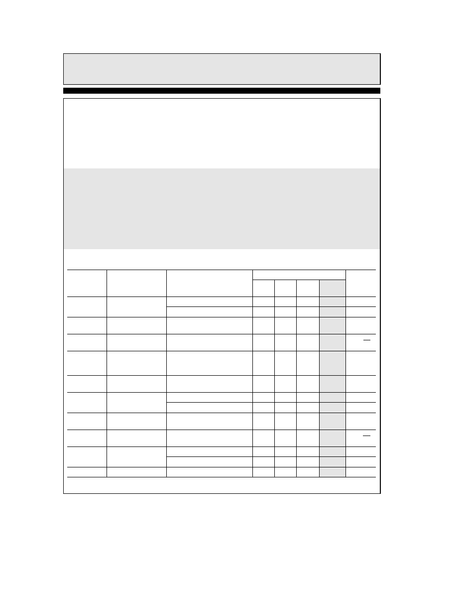
DC Electrical Characteristics
V
S
e
g
15V T
MIN
s
T
A
s
T
MAX
C
C
e
3000 pF
Parameter
Description
Test Conditions
ELH0041
Units
Min
Typ
Max
Test
Level
V
OS
Input Offset Voltage
R
S
s
100
X T
A
e
25 C (Note 4)
1
3
I
mV
R
S
s
100
X (Note 4)
5
I
mV
DV
OS
DT
Voltage Drift
R
S
s
100
X
3
V
mV C
with Temperature
Offset Voltage Drift
T
A
e
25 C
5
V
mV
0
wk
with Time
DV
OS
DP
Offset Voltage
Change with
15
V
mV W
Output Power
Offset Voltage
20
V
mV
Adjustment Range
I
OS
Input Offset Current
T
A
e
25 C (Note 4)
30
100
I
nA
(Note 4)
300
I
nA
Offset Current Drift
0 1
1
IV
nA C
with Temperature
Offset Current Drift
T
A
e
25 C
2
V
nA
0
wk
with Time
I
B
Input Bias
T
A
e
25 C (Note 4)
100
300
I
nA
Current
(Note 4)
1
I
mA
R
IN
Input Resistance
T
A
e
25 C
0 3
1
I
M
X
2
TD
is
39in

ELH0041G 883 8508701ZX
0 1 Amp Power Operational Amplifier
DC Electrical Characteristics
V
S
e
g
15V T
MIN
s
T
A
s
T
MAX
C
C
e
3000 pF
Contd
Parameter
Description
Test Conditions
ELH0041
Units
Min
Typ
Max
Test
Level
CMRR
Common-Mode
R
S
s
100
X V
CM
e
g
10V
70
90
I
dB
Rejection Ratio
V
INCM
Input Voltage Range
g
12
IV
V
PSRR
Power Supply
R
S
s
100
X V
S
e
g
5V to
g
15V
80
96
I
dB
Rejection Ratio
A
V
Voltage Gain
V
O
e
g
10V R
L
e
1 k
X T
A
e
25 C
100
200
I
V mV
(Note 5)
V
O
e
g
10V R
L
e
100
X
25
I
V mV
V
O
Output Voltage Swing
R
L
e
100
X
g
13
14
I
V
I
SC
Output Short
T
A
e
25 C R
SC
e
3 3
X
200
300
I
mA
Circuit Current
I
S
Supply Current
V
OUT
e
0V
2 5
3 5
I
mA
P
C
Power Consumption
V
OUT
e
0V
75
105
I
mW
Note 1 Rating applies for supply voltages above
g
15V For supplies less than
g
15V rating is equal to supply voltage
Note 2 Rating applies for LH0041G with R
SC
e
0
X
Note 3 Rating applies as long as package power rating is not exceeded
Note 4 Specifications apply for
g
5V
s
V
S
s
18V
Note 5 The ELH0041 like all Class B amplifiers has a ``dead band'' when V
OUT
is near zero volts Typical values for the ``dead
band'' are in the 50
mV to 200 mV range Open-loop gain is measured at V
OUT
from
g
0 5 V
DC
to
g
10 V
DC
which is out of
the range of the ``dead band''
AC Electrical Characteristics
T
A
e
25 C V
S
e
g
15V C
C
e
3000 pF
Parameter
Description
Test Conditions
ELH0041
Units
Min
Typ
Max
Test
Level
SR
Slew Rate
A
V
e
1 R
L
e
100
X
1 5
3
I
V
ms
BW
Bandwidth
R
L
e
100
X
20
V
kHz
t
r
t
f
Small Signal
0 3
1
I
ms
Rise or Fall Time
Small Signal Overshoot
5
20
I
%
t
S
Settling Time (0 1%)
DV
IN
e
10V A
V
e
1
4
V
ms
Overload Recovery Time
3
V
ms
HD
Harmonic Distortion
f
e
1 kHz P
O
e
0 5W
0 2
V
%
E
N
Input Noise Voltage
R
S
e
50
X BW
e
10 Hz to 10 kHz
5
V
mV
rms
I
N
Input Noise Current
BW
e
10 Hz to 10 kHz
0 05
V
nA
rms
C
IN
Input Capacitance
3
V
pF
3
TD
is
26in
TD
is
25in

ELH0041G 883 8508701ZX
0 1 Amp Power Operational Amplifier
Typical Performance Curves
Dissipation
Maximum Power
Output Voltage Swing
Open-Loop Frequency
Response
Pulse Response
Large Signal
Pulse Response
Voltage Follower
No Load Supply Current
vs Temperature
Short Circuit Current
Input Bias Current
Voltage Gain
0041 ≠ 4
4

ELH0041G 883 8508701ZX
0 1 Amp Power Operational Amplifier
Typical Performance Curves
Contd
Input Current
Input Voltage Range
Input Noise Voltage
Input Noise Current
Distortion vs Frequency
0041 ≠ 5
Typical Applications
Two Way Intercom
0041 ≠ 6
Programmable High Current Source Sink
0041 ≠ 7
I
OUT
e
V
IN
R5
R2
R1
J
a
V
OUT
R1
a
R2
e
20 mA V
IN
5