 | –≠–ª–µ–∫—Ç—Ä–æ–Ω–Ω—ã–π –∫–æ–º–ø–æ–Ω–µ–Ω—Ç: EL2072CS | –°–∫–∞—á–∞—Ç—å:  PDF PDF  ZIP ZIP |
EL2072C
December
1995
Rev
E
EL2072C
730 MHz Closed Loop Buffer
Note All information contained in this data sheet has been carefully checked and is believed to be accurate as of the date of publication however this data sheet cannot be a ``controlled document'' Current revisions if any to these
specifications are maintained at the factory and are available upon your request We recommend checking the revision level before finalization of your design documentation
1991 Elantec Inc
Features
730 MHz
b
3 dB bandwidth
(0 5 V
PP
)
5 ns settling to 0 2%
V
S
e
g
5V
15 mA
Low distortion HD2 HD3 of
b
65 dBc at 20 MHz
Overload short-circuit protected
Closed-loop unity gain
Low cost
Direct replacement for CLC110
Applications
Video buffer
Video distribution
HDTV buffer
High-speed A D buffer
Photodiode CCD preamps
IF processors
High-speed communications
Ordering Information
Part No
Temp Range
Package
Outline
EL2072CN
b
40 C to
a
85 C
8-Pin P-DIP
MDP0031
EL2072CS
b
40 C to
a
85 C
8-Pin SO
MDP0027
General Description
The EL2072 is a wide bandwidth fast settling monolithic buffer
built using an advanced complementary bipolar process This
buffer is closed loop to achieve lower output impedance and
higher gain accuracy Designed for closed-loop unity gain the
EL2072 has a 730 MHz
b
3 dB bandwidth and 5 ns settling to
0 2% while consuming only 15 mA of supply current
The EL2072 is an obvious high-performance solution for video
distribution and line-driving applications With low 15 mA sup-
ply current and a 70 mA output drive performance in these
areas is assured
The EL2072's settling to 0 2% in 5 ns low distortion and abili-
ty to drive capacitive loads make it an ideal flash A D driver
The wide 730 MHz bandwidth and extremely linear phase allow
unmatched signal fidelity
The EL2072 can be used inside an amplifier loop or PLL as its
wide bandwidth and fast rise time have minimal effect on loop
dynamics
Elantec products and facilities comply with MIL-I-45028A and
other applicable quality specifications
For information on
Elantec's processing see Elantec document QRA-1 Elantec's
Processing Monolithic Integrated Circuits
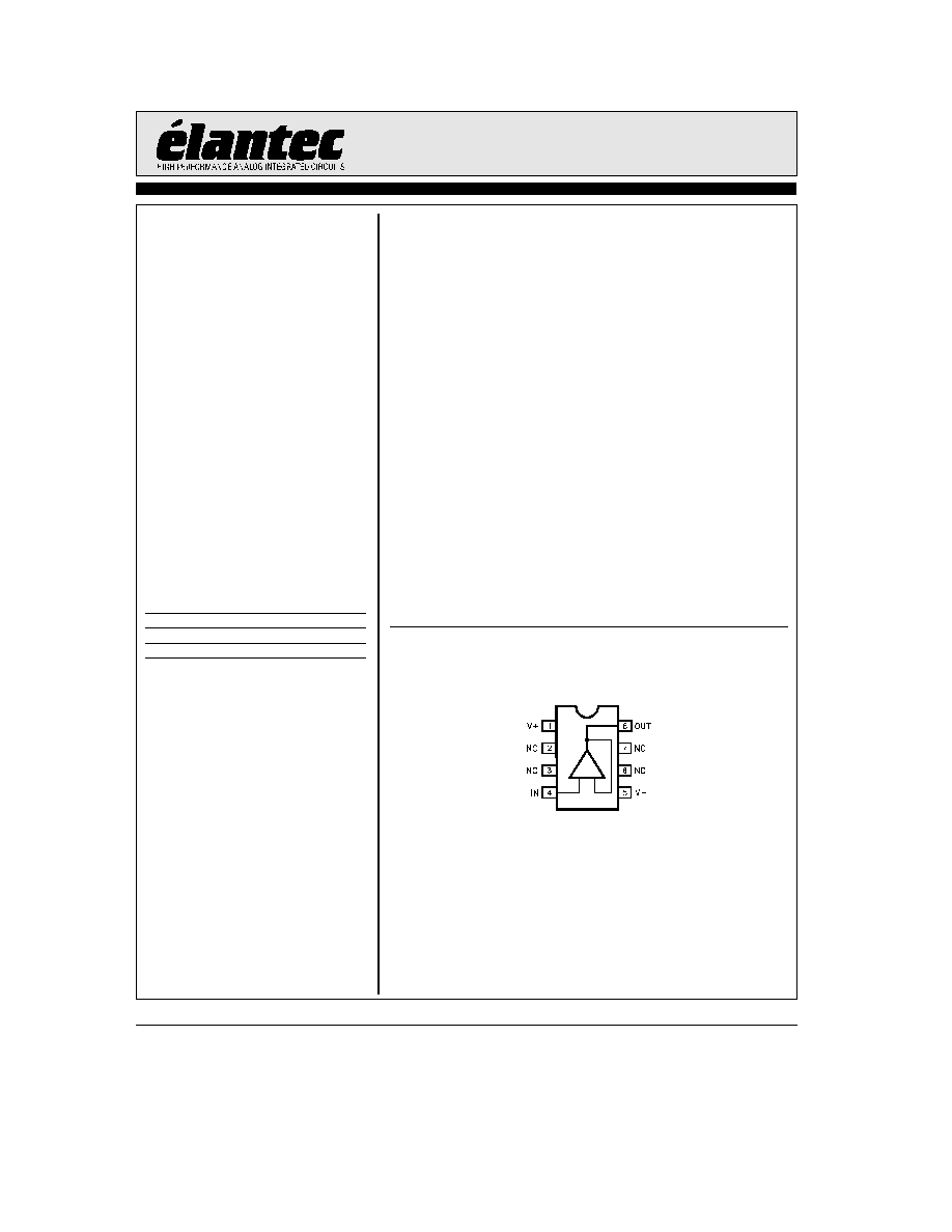
Connection Diagram
DIP and SO Package
2072 ≠ 1
Top View
Manufactured under U S Patent No 4 893 091

EL2072C
730 MHz Closed Loop Buffer
Absolute Maximum Ratings
(T
A
e
25 C)
Supply Voltage (V
S
)
g
7V
Output Current
Output is short-circuit protect-
ed to ground however maxi-
mum reliability is obtained if
I
OUT
does not exceed 70 mA
Input Voltage
g
V
S
Operating Temperature
b
40 C to
a
85 C
Junction Temperature
175 C
Storage Temperature
b
60 C to
a
150 C
Thermal Resistance
i
JA
e
95 C W P-DIP
i
JA
e
175 C W SO
Note See EL2071 EL2171 for Thermal Impedance curves
Important Note
All parameters having Min Max specifications are guaranteed The Test Level column indicates the specific device testing actually
performed during production and Quality inspection Elantec performs most electrical tests using modern high-speed automatic test
equipment specifically the LTX77 Series system Unless otherwise noted all tests are pulsed tests therefore T
J
e
T
C
e
T
A
Test Level
Test Procedure
I
100% production tested and QA sample tested per QA test plan QCX0002
II
100% production tested at T
A
e
25 C and QA sample tested at T
A
e
25 C
T
MAX
and T
MIN
per QA test plan QCX0002
III
QA sample tested per QA test plan QCX0002
IV
Parameter is guaranteed (but not tested) by Design and Characterization Data
V
Parameter is typical value at T
A
e
25 C for information purposes only
DC Electrical Characteristics
V
S
e
g
5V R
L
e
100
X R
S
e
50
X unless otherwise specified
Parameter
Description
Test
Temp
Min
Typ
Max
Test
Units
Conditions
Level
V
OS
Output Offset Voltage
25 C
2 0
8 0
I
mV
T
MIN
16 0
V
mV
T
MAX
13 0
V
mV
TCV
OS
Average Offset
25 C
b
T
MAX
20 0
50 0
IV
mV C
Voltage Drift
25 C
b
T
MIN
20 0
100 0
I
B
Input Bias Current
25 C T
MAX
10 0
50 0
II
mA
T
MIN
100 0
V
mA
TCI
B
Average Input Bias
25 C
b
T
MAX
200 0
300 0
IV
nA C
Current Drift
25 C
b
T
MIN
200 0
700 0
A
V
Small Signal Gain
R
L
e
100
X
25 C
0 96
0 98
I
V V
T
MIN
T
MAX
0 95
V
V V
ILIN
Integral End
g
2V F S
25 C
0 2
0 4
IV
%F S
Point linearity
T
MIN
0 8
IV
%F S
T
MAX
0 3
IV
%F S
PSRR
Power Supply
All
45 0
65 0
II
dB
Rejection Ratio
I
S
Supply Current
Quiescent
No Load
All
15 0
20 0
II
mA
2
TD
is
33in
EL2072C
730 MHz Closed Loop Buffer
DC Electrical Characteristics
V
S
e
g
5V R
L
e
100
X R
S
e
50
X unless otherwise specified
Contd
Parameter
Description
Test
Temp
Min
Typ
Max
Test
Units
Conditions
Level
R
IN
Input Resistance
25 C
100 0
160 0
I
k
X
T
MIN
50 0
V
k
X
T
MAX
200 0
V
k
X
C
IN
Input Capacitance
25 C
1 6
2 2
IV
pF
T
MIN
T
MAX
2 5
IV
pF
R
OUT
Output Impedance (DC)
25 C
2 0
3 0
IV
X
T
MIN
T
MAX
3 5
IV
X
I
OUT
Output Current
25 C T
MAX
50 0
70 0
II
mA
T
MIN
45 0
V
mA
V
OUT
Output Voltage Swing
R
L
e
100
X
25 C T
MAX
g
3 2
g
4 0
II
V
T
MIN
g
3 0
V
V
AC Electrical Characteristics
V
S
e
g
5V R
L
e
100
X R
S
e
50
X unless otherwise specified
Parameter
Description
Test
Temp
Min
Typ
Max
Test
Units
Conditions
Level
FREQUENCY RESPONSE
SSBW
b
3 dB Bandwidth
25 C
400 0
730 0
V
MHz
(V
OUT
k
0 5 V
PP
)
T
MIN
400 0
IV
MHz
T
MAX
300 0
IV
MHz
LSBW
b
3 dB Bandwidth
25 C
55 0
90 0
IV
MHz
(V
OUT
e
5 0 V
PP
)
T
MIN
T
MAX
50 0
IV
MHz
GAIN FLATNESS
GFPL
Peaking
k
200 MHz
25 C
0 0
0 5
V
dB
V
OUT
k
0 5 V
PP
T
MAX
0 6
IV
dB
T
MIN
0 8
IV
dB
GFR
Rolloff
k
200 MHz
25 C
0 0
0 8
V
dB
V
OUT
k
0 5 V
PP
T
MIN
1 0
IV
dB
T
MAX
1 2
IV
dB
GDL
Group Delay
k
200 MHz
25 C T
MIN
0 75
1 0
IV
ns
T
MAX
1 2
IV
ns
LPD
Linear Phase Deviation
k
200 MHz
25 C T
MIN
0 7
1 5
IV
V
OUT
k
0 5 V
PP
T
MAX
2 0
IV
3
TD
is
24in
TD
is
35in

EL2072C
730 MHz Closed Loop Buffer
AC Electrical Characteristics
Contd
V
S
e
g
5V R
L
e
100
X R
S
e
50
X unless otherwise specified
Parameter
Description
Test
Temp
Min
Typ
Max
Test
Units
Conditions
Level
TIME-DOMAIN RESPONSE
TR1 TF1
Rise Time Fall Time
0 5V Step
25 C T
MIN
0 4
1 0
IV
ns
Input Signal Rise Fall
e
300 ps
T
MAX
1 4
IV
ns
TR2 TF2
Rise Time Fall Time
5 0V Step
25 C
4 5
7 5
IV
ns
Input Signal Rise Fall
s
1 ns
T
MIN
T
MAX
8 5
IV
ns
TS1
Settling Time to 0 2%
2 0V Step
All
5 0
10 0
IV
ns
Input Signal Rise Fall
s
1 ns
OS
Overshoot
0 5V Step
25 C
0 0
10 0
IV
%
Input Signal Rise Fall
e
300 ps
T
MIN
T
MAX
15 0
IV
%
SR
Slew Rate
25 C
500 0
800 0
IV
V
ms
T
MIN
T
MAX
450 0
IV
V
ms
DISTORTION
HD2
2nd Harmonic Distortion
2 V
PP
25 C
b
55 0
b
50 0
V
dBc
at 20 MHz
T
MIN
b
48 0
IV
dBc
T
MAX
b
55 0
IV
dBc
HD2A
2nd Harmonic Distortion
2 V
PP
25 C T
MAX
b
50 0
b
45 0
IV
dBc
at 50 MHz
T
MIN
b
40 0
IV
dBc
HD3
3rd Harmonic Distortion
2 V
PP
25 C
b
65 0
b
55 0
V
dBc
at 20 MHz
T
MIN
T
MAX
b
55 0
IV
dBc
HD3A
3rd Harmonic Distortion
2 V
PP
25 C T
MIN
b
60 0
b
50 0
IV
dBc
at 50 MHz
T
MAX
b
45 0
IV
dBc
EQUIVALENT INPUT NOISE
NF
Noise Floor
25 C T
MIN
b
158 0
b
155 0
IV
dBm (1 Hz)
l
100 kHz
T
MAX
b
154 0
IV
dBm (1 Hz)
INV
Integrated Noise
25 C T
MIN
40 0
57 0
IV
mV
100 kHz to 200 MHz
T
MAX
63 0
IV
mV
4
TD
is
51in

EL2072C
730 MHz Closed Loop Buffer
Typical Performance Curves
(V
S
e
g
5V R
L
e
100
X R
S
e
50
X)
Forward Gain and Phase
from Linear Phase
Gain Flatness
Deviation
Reverse Gain and phase
Input Impedance
Output Impedance
Load Capacitance
Recommended R
S
vs
Integral Linearity Error
Frequency Response vs R
load
with Recommended R
s
l
S
21
l
vs C
load
2072 ≠ 2
5